EP1001432A1 - Prüfungsverfahren eines dynamischen Speichers - Google Patents
Prüfungsverfahren eines dynamischen Speichers Download PDFInfo
- Publication number
- EP1001432A1 EP1001432A1 EP98309192A EP98309192A EP1001432A1 EP 1001432 A1 EP1001432 A1 EP 1001432A1 EP 98309192 A EP98309192 A EP 98309192A EP 98309192 A EP98309192 A EP 98309192A EP 1001432 A1 EP1001432 A1 EP 1001432A1
- Authority
- EP
- European Patent Office
- Prior art keywords
- location
- test
- data
- register
- stored
- Prior art date
- Legal status (The legal status is an assumption and is not a legal conclusion. Google has not performed a legal analysis and makes no representation as to the accuracy of the status listed.)
- Withdrawn
Links
- 238000010998 test method Methods 0.000 title claims abstract 4
- 238000012360 testing method Methods 0.000 claims abstract description 58
- 238000000034 method Methods 0.000 claims abstract description 25
- 230000000295 complement effect Effects 0.000 claims description 4
- 238000007796 conventional method Methods 0.000 abstract description 4
- 238000010586 diagram Methods 0.000 description 2
- 230000002411 adverse Effects 0.000 description 1
- 230000000694 effects Effects 0.000 description 1
Images

Classifications
-
- G—PHYSICS
- G11—INFORMATION STORAGE
- G11C—STATIC STORES
- G11C29/00—Checking stores for correct operation ; Subsequent repair; Testing stores during standby or offline operation
- G11C29/52—Protection of memory contents; Detection of errors in memory contents
-
- G—PHYSICS
- G11—INFORMATION STORAGE
- G11C—STATIC STORES
- G11C29/00—Checking stores for correct operation ; Subsequent repair; Testing stores during standby or offline operation
- G11C29/04—Detection or location of defective memory elements, e.g. cell constructio details, timing of test signals
- G11C29/08—Functional testing, e.g. testing during refresh, power-on self testing [POST] or distributed testing
- G11C29/10—Test algorithms, e.g. memory scan [MScan] algorithms; Test patterns, e.g. checkerboard patterns
Definitions
- This invention relates to methods of testing random-access memory (RAM) without destroying the data stored in the memory.
- the conventional method of testing RAM is to cycle though all the addresses to be tested, and for each address to write a first test pattern consisting of a series of alternating ones and zeroes to the address and to compare what is actually stored at the address with the first test pattern and then to write a second test pattern consisting of the complementary series of alternating zeroes and ones to the address and to compare what is actually stored at the address with the second complementary test pattern. If any of the comparisons fails, the test fails and can be aborted at that point; if none of them fails the test succeeds.
- the invention is as set out in claim 1.
- each bit at the address being tested is changed twice, once when the original data word is inverted and once when the twice-inverted data word is written back to the address.
- the comparison will fail unless both changes are correctly made.
- the method contains only two write operations in addition to three read operations and only has one comparison instruction and one conditional jump.
- exemplary data words will be illustrated as containing eight bits, for the sake of simplicity. As will be appreciated, sixteen or 32 bits is a more usual number and the method does not depend on the number of bits in a data word.
- the conventional method starts at the first address to be tested (1).
- the data word stored at that address is first loaded into a register (2) and a first test pattern such as 10101010 is written to the addressed location (3).
- the actual content of the location is then compared with the first test pattern (4) and if they do not agree the test is failed (5).
- a second test pattern complementary to the first, such as 01010101, is written to the location (6) and the actual content of the location compared with the second test pattern (7). Once again, if they do not agree the test is failed (8).
- this method Since each bit has been set to “1” and to "0" by the test patterns and tested, this method will detect any bit that is stuck at either “0” or “1". However, it will not reliably detect a condition in which a bit can be changed one way but not restored to its original value. For example, if the third bit was originally equal to "1" and could be cleared to "0” but not reset to “1” the first test pattern would not change it, so the first comparison 4 would indicate agreement, and the second test pattern could change it to "0", so the second comparison would also indicate agreement. Furthermore this method involves three write-to-memory operations, namely steps 3, 6 and 9 in addition to three read operations, namely the load to register step 2 and the two comparison steps 4 and 7.
- the first address to be tested contains the word 10110110.
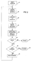
- the testing method starts with the first address to be tested (21) and inverts all of the bits in the word stored at that address (22).
- the addressed location now contains the word 01001001.
- That word is now loaded into a register of the microprocessor controlling the testing method (23).
- This register now also contains the word 01001001.
- all of the bits in the register are inverted (24), so the register now contains the word 10110110 which, since two inversions have been carried out, is the same as the word originally stored at the addressed location.
- the word in the register is written back to the addressed location (25), which now contains the originally stored word, and the contents of the addressed location are compared with the contents of the register (26). If they are not equal, the test is failed, and may be stopped (27). However, under our assumption that the memory is working, they are equal, so the method proceeds to the next address (29) and repeats the test. When the last address has been tested (28), no failures having taken place, the method terminates (30), the memory having passed the test.
- the addressed location being tested now contains the word 10110110 as before, but after the first inversion step 22 it contains the word 01101001 since the third digit, which is a "1", sticks at the same value.
- the register contains the word 10010110.
- the third digit is a "0" rather than a "1” as before.
- the location actually contains the word 10110110 again, rather that 10010110 as contained in the register, since the third bit is still stuck to "1". Since the contents of the addressed location are different from those of the register the comparison step 26 gives a "NO" result and the test is failed (27).
- each bit must be successfully changed and changed back again.
- the test is failed not only if a bit cannot be changed (is stuck) but if, having been changed, it cannot be restored to its original value.
- the method contains only two write-to-memory operations, namely the first inversion step 22, which is a read-and-write step, and the writing back step 25. This leads to a considerable speed advantage, since the test has to be carried out on a large number of locations. This is especially important when the method is to be carried out periodically as a background process with minimum adverse effect on other processing.
- test patterns consisting of alternating "1"s and "0"s the conventional method can detect cases in which there we short circuits between odd and even data bus leads, so that setting one bit will affect an adjacent bit. If this is happening at all, however, it will not only happen at one memory location but all of them, so it could be tested for by carrying out a test at a selected location. This could consist of carrying out the conventional test, but it would not add appreciably to the system load, since it would not have to be repeated for every location. Better still, a series of test patterns could be used to test for short circuits between any pair of bus leads, not just adjacent ones.
- Such a series of test patterns could, for example, consist of 10101010, 11001100, 11110000 and soon (for a word with more than eight bits).
- n patterns if the number of bits in a word were 2 n .
- These patterns would consist of alternating groups of 2 m "1"s and 2 m "0"s, where m is in the range 0 to n - 1.
Landscapes
- Techniques For Improving Reliability Of Storages (AREA)
Priority Applications (2)
| Application Number | Priority Date | Filing Date | Title |
|---|---|---|---|
| EP98309192A EP1001432A1 (de) | 1998-11-10 | 1998-11-10 | Prüfungsverfahren eines dynamischen Speichers |
| US09/437,409 US6567940B1 (en) | 1998-11-10 | 1999-11-10 | Method of testing random-access memory |
Applications Claiming Priority (1)
| Application Number | Priority Date | Filing Date | Title |
|---|---|---|---|
| EP98309192A EP1001432A1 (de) | 1998-11-10 | 1998-11-10 | Prüfungsverfahren eines dynamischen Speichers |
Publications (1)
| Publication Number | Publication Date |
|---|---|
| EP1001432A1 true EP1001432A1 (de) | 2000-05-17 |
Family
ID=8235157
Family Applications (1)
| Application Number | Title | Priority Date | Filing Date |
|---|---|---|---|
| EP98309192A Withdrawn EP1001432A1 (de) | 1998-11-10 | 1998-11-10 | Prüfungsverfahren eines dynamischen Speichers |
Country Status (2)
| Country | Link |
|---|---|
| US (1) | US6567940B1 (de) |
| EP (1) | EP1001432A1 (de) |
Cited By (2)
| Publication number | Priority date | Publication date | Assignee | Title |
|---|---|---|---|---|
| EP1750283A3 (de) * | 2005-08-04 | 2007-08-22 | Robert Bosch Gmbh | Überprüfung eines Adressdecoders |
| EP2660052A1 (de) | 2012-04-30 | 2013-11-06 | Neopack, S.L. | System und Verfahren zur Befestigung eines bedruckbaren Bahnsubstrats auf einem zentralen Druckzylinder einer Druckmaschine, und Druckmaschine mit diesem System |
Families Citing this family (6)
| Publication number | Priority date | Publication date | Assignee | Title |
|---|---|---|---|---|
| JP2004185060A (ja) * | 2002-11-29 | 2004-07-02 | Renesas Technology Corp | マイクロコンピュータ |
| US7818625B2 (en) * | 2005-08-17 | 2010-10-19 | Microsoft Corporation | Techniques for performing memory diagnostics |
| US8427854B2 (en) | 2010-04-15 | 2013-04-23 | Microsoft Corporation | Utilization of memory refresh cycles for pattern matching |
| JP2012073678A (ja) * | 2010-09-27 | 2012-04-12 | Fujitsu Ltd | 擬似エラー発生装置 |
| US10203893B2 (en) | 2015-10-22 | 2019-02-12 | American Megatrends, Inc. | Memory channel storage device detection |
| US10558468B2 (en) | 2015-10-22 | 2020-02-11 | American Megatrends International, Llc | Memory channel storage device initialization |
Citations (1)
| Publication number | Priority date | Publication date | Assignee | Title |
|---|---|---|---|---|
| US5699508A (en) * | 1991-10-16 | 1997-12-16 | Alps Electric (Usa), Inc. | Keyboard testing methods and apparatus |
Family Cites Families (2)
| Publication number | Priority date | Publication date | Assignee | Title |
|---|---|---|---|---|
| US5034923A (en) * | 1987-09-10 | 1991-07-23 | Motorola, Inc. | Static RAM with soft defect detection |
| US5471482A (en) * | 1994-04-05 | 1995-11-28 | Unisys Corporation | VLSI embedded RAM test |
-
1998
- 1998-11-10 EP EP98309192A patent/EP1001432A1/de not_active Withdrawn
-
1999
- 1999-11-10 US US09/437,409 patent/US6567940B1/en not_active Expired - Lifetime
Patent Citations (1)
| Publication number | Priority date | Publication date | Assignee | Title |
|---|---|---|---|---|
| US5699508A (en) * | 1991-10-16 | 1997-12-16 | Alps Electric (Usa), Inc. | Keyboard testing methods and apparatus |
Cited By (3)
| Publication number | Priority date | Publication date | Assignee | Title |
|---|---|---|---|---|
| EP1750283A3 (de) * | 2005-08-04 | 2007-08-22 | Robert Bosch Gmbh | Überprüfung eines Adressdecoders |
| US7954042B2 (en) | 2005-08-04 | 2011-05-31 | Robert Bosch Gmbh | Check testing of an address decoder |
| EP2660052A1 (de) | 2012-04-30 | 2013-11-06 | Neopack, S.L. | System und Verfahren zur Befestigung eines bedruckbaren Bahnsubstrats auf einem zentralen Druckzylinder einer Druckmaschine, und Druckmaschine mit diesem System |
Also Published As
| Publication number | Publication date |
|---|---|
| US6567940B1 (en) | 2003-05-20 |
Similar Documents
| Publication | Publication Date | Title |
|---|---|---|
| US5502732A (en) | Method for testing ECC logic | |
| EP0529945B1 (de) | Verfahren und Gerät zur programmierbaren Speicherssteuerung mit Fehlerregelung und Prüffunktionen | |
| EP0447995A2 (de) | Analysevorrichtung zur Rettung von Halbleiterspeicherfehlern | |
| DE102005048255A1 (de) | Integriertes Schaltungsbauelement und Betriebsverfahren | |
| US4891811A (en) | Efficient address test for large memories | |
| KR20010037848A (ko) | 반도체 메모리 장치 및 이 장치의 병렬 비트 테스트 방법 | |
| US5541942A (en) | Method and system for testing memory utilizing specific bit patterns | |
| EP0448970A2 (de) | Ein Informationsverarbeitungsgerät mit einer Fehlerprüf- und Korrekturschaltung | |
| US7966531B2 (en) | Memory diagnosis apparatus | |
| EP0031706B1 (de) | Vorrichtung und Verfahren zum Prüfen von Halbleiterspeicherbausteinen | |
| US4368532A (en) | Memory checking method | |
| EP1001432A1 (de) | Prüfungsverfahren eines dynamischen Speichers | |
| US6237116B1 (en) | Testing error correcting code feature in computers that do not have direct hardware features for causing single bit and multi-bit errors | |
| US5822513A (en) | Method and apparatus for detecting stale write data | |
| US4696005A (en) | Apparatus for reducing test data storage requirements for high speed VLSI circuit testing | |
| JPS6237422B2 (de) | ||
| US6539338B1 (en) | Self-diagnostic testing of a network interface adapter | |
| US20130124925A1 (en) | Method and apparatus for checking a main memory of a processor | |
| US5146458A (en) | Data transfer checking system | |
| US7320096B2 (en) | System and method for testing memory at full bandwidth | |
| CN119829168B (zh) | 用于编程操作的数据验证方法及装置、电子设备 | |
| JPH0452842A (ja) | メモリチェック方式 | |
| JPH0528058A (ja) | メモリアドレスバス試験方式 | |
| EP0127350B1 (de) | Magnetblasenspeichergerät | |
| SU896626A1 (ru) | Устройство дл контрол ввода-вывода |
Legal Events
| Date | Code | Title | Description |
|---|---|---|---|
| PUAI | Public reference made under article 153(3) epc to a published international application that has entered the european phase |
Free format text: ORIGINAL CODE: 0009012 |
|
| AK | Designated contracting states |
Kind code of ref document: A1 Designated state(s): DE FR GB NL |
|
| AX | Request for extension of the european patent |
Free format text: AL;LT;LV;MK;RO;SI |
|
| 17P | Request for examination filed |
Effective date: 20001106 |
|
| AKX | Designation fees paid |
Free format text: DE FR GB NL |
|
| GRAP | Despatch of communication of intention to grant a patent |
Free format text: ORIGINAL CODE: EPIDOSNIGR1 |
|
| STAA | Information on the status of an ep patent application or granted ep patent |
Free format text: STATUS: THE APPLICATION IS DEEMED TO BE WITHDRAWN |
|
| 18D | Application deemed to be withdrawn |
Effective date: 20030531 |