EP1001460B1 - Procédé et appareil pour détecter, surveiller et caractériser des défauts de bordure sur les plaquettes semiconductrices - Google Patents
Procédé et appareil pour détecter, surveiller et caractériser des défauts de bordure sur les plaquettes semiconductrices Download PDFInfo
- Publication number
- EP1001460B1 EP1001460B1 EP98119508A EP98119508A EP1001460B1 EP 1001460 B1 EP1001460 B1 EP 1001460B1 EP 98119508 A EP98119508 A EP 98119508A EP 98119508 A EP98119508 A EP 98119508A EP 1001460 B1 EP1001460 B1 EP 1001460B1
- Authority
- EP
- European Patent Office
- Prior art keywords
- wafer
- edge
- infrared
- laser beam
- monitoring
- Prior art date
- Legal status (The legal status is an assumption and is not a legal conclusion. Google has not performed a legal analysis and makes no representation as to the accuracy of the status listed.)
- Expired - Lifetime
Links
Images



Classifications
-
- G—PHYSICS
- G01—MEASURING; TESTING
- G01N—INVESTIGATING OR ANALYSING MATERIALS BY DETERMINING THEIR CHEMICAL OR PHYSICAL PROPERTIES
- G01N21/00—Investigating or analysing materials by the use of optical means, i.e. using sub-millimetre waves, infrared, visible or ultraviolet light
- G01N21/84—Systems specially adapted for particular applications
- G01N21/88—Investigating the presence of flaws or contamination
- G01N21/95—Investigating the presence of flaws or contamination characterised by the material or shape of the object to be examined
- G01N21/9501—Semiconductor wafers
- G01N21/9503—Wafer edge inspection
-
- H—ELECTRICITY
- H10—SEMICONDUCTOR DEVICES; ELECTRIC SOLID-STATE DEVICES NOT OTHERWISE PROVIDED FOR
- H10P—GENERIC PROCESSES OR APPARATUS FOR THE MANUFACTURE OR TREATMENT OF DEVICES COVERED BY CLASS H10
- H10P74/00—Testing or measuring during manufacture or treatment of wafers, substrates or devices
- H10P74/20—Testing or measuring during manufacture or treatment of wafers, substrates or devices characterised by the properties tested or measured, e.g. structural or electrical properties
- H10P74/203—Structural properties, e.g. testing or measuring thicknesses, line widths, warpage, bond strengths or physical defects
Definitions
- edge crown, bevels and near-to-edge wafer defects such as scratches, grooves, cracks and chips can dramatically reduce the performance of ULSI structures in electronic devices.
- the visual, non-contact inspection of the edge, all-around the wafer, at different stages of wafer processing, such as slicing, lapping, edge-shaping, grinding, etching, and polishing is generally performed by trained operators, under a bright light, with a naked eye or with a magnifier lens.
- the reflected light that contains information about the edge defects is captured by the video camera and displayed on a TV monitor.
- the light source and the video camera are always on the same side of the inspected edge, as shown in Fig.1 representing a so-called reflective configuration (R-configuration), and the light source spectrum is always in the visible domain (400 to 700 nm).
- EP-766 298 A2 discloses a method and an apparatus for determining residual crystal damages caused to wafer edges by an optical-acoustical process.
- EP-468 817 A2 concerns an infrared scanning microscope and a method of assessing a polished surface of a semiconductor specimen using the infrared scanning microscope.
- EP-100 446 A1 refers to a high resolution automatic imaging and inspecting system for shape dimensional inspection and for defect detection on edges of small articles.
- EP-120 211 A2 is related to a method and an apparatus for the dimensional checking of solid bodies with a laser beam.
- the above object is achieved according to the present invention by a method for detecting, monitoring and characterizing edge defects on semiconductor wafers, comprising illuminating the edge of a wafer with an infrared laser beam, the wafer being tilted with respect to the laser beam; and inspecting the illuminated wafer edge with at least one infrared video camera.
- an apparatus for detecting, monitoring and characterizing edge defects on semiconductor wafers comprising an infrared illumination system illuminating the wafer edge with an infrared laser beam; a tiltable platform presenting the wafer in a tilted manner with respect to the infrared laser beam; and at least one infrared video camera monitoring the illuminated wafer edge.
- the reflected light intensity emerging from a specimen may be influenced by any combination of light absorption, scattering, diffraction and distortion.
- Light scattered by particles and crystalline defects on the edge may have a negative image distortion impact on the specular reflected energy which contains edge defect shape information.
- light absorption may be significant under the same conditions; as deep the incident laser beam enters the edge surface, as much defect information is obtained.
- the size, scattering and absorptive characteristics of the semiconductor material defect or edge contaminant play a combined role in the reflected image.
- an infrared laser illumination source for illuminating the wafer edge and an infrared sensitive camera for monitoring wafer edge defects is used. It is particularly preferred to illuminate the wafer edge with a multi-wavelangth laser, e.g. a Yag-Nd green laser, with a three wavelength laser beam, two of them in the near-infrared domain (806 nm and 1064 nm), and one in the green range (532 nm). Using a filter wheel, one, two or all three of these wavelength combination may be selected when inspecting the wafer edge. This laser feature increases the edge defects visualization. An infrared sensitive CCD video camera will be used for inspection.
- a multi-wavelangth laser e.g. a Yag-Nd green laser
- a wafer tilt angle of preferable 30 to 45 degrees from horizontal allows a better view of the bevel and an uniform illumination of it and the detection of bevel-near-to-surface microchips and microcracks, responsible for epitaxial-layers-defects.
- the apparatus configuration according to Fig.2 is particularly suitable for detecting edge cracks that pass from one edge side to the other side.
- infrared laser beam transmissive configuration T-configuration
- the laser beam impinges the specimen from the opposite side, and the infrared rays that pass through the cracks are visible as second sources of light by the camera.
- Using the transmissive configuration is then possible to isolate the microcracks, that almost likely generate wafer breakage, from larger category of edge chips and grinding wheel grooves defects.
- the reflective and the transmissive configuration are implemented with a unique configuration (one camera R/T-configuration).
- This configuration further comprises two diffusive, rotatable deflectors, which create an uniform laser beam illumination area by the inspected wafer edge, and a rotatable prism, which allows to target the edge and the deflectors, simultaneously.
- the one-camera R/T configuration is able to facilitate a complete view of the edge and its front side bevel, facing the camera. The camera view covers more than half of the entire wafer's edge area.
- Fig.4 shows this two-camera R/T configuration.
- two distinct cameras are provided, camera 1 covering more than half of the entire edge, plus a small sector of the front surface, and a second camera 2, covering the remaining edge half.
- the information provided by camera 1, facing edge and bevel will contain information resulted both by reflection, scattering and diffusion of the laser beam, and by transmission of the same laser beam through the edge cracks, from the backside to the front side of the wafer.
- the information provided by camera 2 will contain information resulted by reflection, scattering and diffusion of the laser beam.
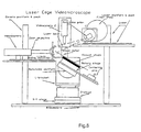
- Fig.5 represents a wafer edge inspecting apparatus, which is constructed in accordance with the two-camera R/T configuration.
- the whole system is supported by an optical breadboard of 300x600 mm.
- the video camera 1, the zoom microscope objective, and the laser beam deflectors are mounted breadboard of 300 ⁇ 600 mm.
- the video camera 1, the zoom microscope objective, and the laser beam deflectors are mounted on sliding carriers, on optic mini rails, installed on a horizontal rotatable platform and rod clamp, which may be lifted on an optic rod.
- the laser source can be lifted on a second optic rod, with a rotatable platform and rod clamp too.
- the laser beam will be directed toward the beam deflector/diffuser using a rotatable prism.
- the wafer chuck is installed on a rotary stage, placed on a rotatable (0 to 45°) platform, on a corner bracket, which is supported by the z and x,y-translation stages.
- a sliding carrier with Teflon® removable pins, which can slide on a tilted mini rail is suitable for centering the wafer on the Teflon ® -coated vacuum chuck.
- Fig. 6 shows the principle of the sliding deflector system for a uniform laser illumination and improved crack detection which is used in the apparatus according to Fig.5.
- This deflector system comprises a sliding deflector, composed of two rotatable deflectors/diffusers.
- the deflector system shown in fig.6 can be replaced by a continuous diffusive hemisphere system as represented in Fig.7.
- This system comprises a diffusive hemisphere, that has two camera access ports for collecting the wafer edge images with two cameras, and a centered diffusive minisphere placed at equal distances from the access ports. Sliding the hemisphere changes the distance D between the minisphere and the wafer's edge.
- the laser beam impinges upon the diffusive minisphere and is uniformly reflected toward the hemisphere and the wafer.
- the laser can be focused on the minisphere, can be moved on it by rotating prism shown in Fig.5, or can be defocused, changing its cross-section in contact with the minisphere.
- the illumination pattern emerging from the hemisphere can be continuously changed from a brightfield source to an uniform diffuse, darkfield/brightfield-shadowfree light source, or even to a directionally darkfield only.
Landscapes
- Physics & Mathematics (AREA)
- Health & Medical Sciences (AREA)
- Life Sciences & Earth Sciences (AREA)
- Chemical & Material Sciences (AREA)
- Analytical Chemistry (AREA)
- Biochemistry (AREA)
- General Health & Medical Sciences (AREA)
- General Physics & Mathematics (AREA)
- Immunology (AREA)
- Pathology (AREA)
- Investigating Materials By The Use Of Optical Means Adapted For Particular Applications (AREA)
- Testing Or Measuring Of Semiconductors Or The Like (AREA)
- Length Measuring Devices By Optical Means (AREA)
Claims (10)
- Procédé pour détecter, surveiller et caractériser les défauts de bordure sur des plaquettes semiconductrices, comprenant l'illumination de la bordure d'une plaquette à l'aide d'un faisceau laser infrarouge, la plaquette étant inclinée par rapport au faisceau laser ; et l'inspection de la bordure de la plaquette illuminée à l'aide d'au moins une caméra vidéo infrarouge.
- Procédé selon la revendication 1, comprenant l'inclinaison de la plaquette par rapport au faisceau laser d'un angle de 30 à 45 degrés.
- Procédé selon la revendication 1 ou la revendication 2, dans lequel la bordure de la plaquette est illuminée à l'aide d'un laser infrarouge à trois longueurs d'onde.
- Procédé selon l'une quelconque des revendications 1 à 3, dans lequel le laser illuminant la bordure de la plaquette et la caméra vidéo sont agencés suivant une configuration transmissive.
- Procédé selon l'une quelconque des revendications 1 à 4, dans lequel le laser illuminant la bordure de la plaquette et la caméra vidéo sont agencés suivant une configuration de réflexion et de transmission combinée.
- Appareil pour détecter, surveiller et caractériser les défauts de bordure sur des plaquettes semiconductrices comprenant un système d'illumination infrarouge illuminant la bordure d'une plaquette à l'aide d'un faisceau laser infrarouge ; une plate-forme inclinable présentant la plaquette d'une manière inclinée par rapport au faisceau laser infrarouge ; et au moins une caméra vidéo infrarouge surveillant la bordure de la plaquette illuminée.
- Appareil selon la revendication 6, dans lequel le système d'illumination infrarouge est un système d'illumination à faisceau laser infrarouge à trois longueurs d'onde.
- Appareil selon la revendication 6 ou la revendication 7, comprenant en outre un système déflecteur coulissant composé de deux déflecteurs / diffuseurs rotatifs qui créent une zone d'illumination uniforme du faisceau laser par la bordure de la plaquette inspectée.
- Appareil selon la revendication 6 ou la revendication 7, comprenant en outre un système déflecteur composé d'un hémisphère diffuseur continu et d'une minisphère diffuseuse pour produire un motif d'illumination variable spécifique émergeant de l'hémisphère.
- Appareil selon l'une des revendications 6 à 9, dans lequel le système d'illumination comprend deux desdites caméras vidéo infrarouge, et la plaquette et les deux desdites caméras vidéo infrarouge sont agencées suivant une configuration à la fois de réflexion et de transmission.
Priority Applications (3)
| Application Number | Priority Date | Filing Date | Title |
|---|---|---|---|
| DE69800756T DE69800756T2 (de) | 1998-10-15 | 1998-10-15 | Verfahren und Vorrichtung zum Detektieren, Überwachung und Charakterisierung von Kantendefekten in Halbleiterscheiben |
| EP98119508A EP1001460B1 (fr) | 1998-10-15 | 1998-10-15 | Procédé et appareil pour détecter, surveiller et caractériser des défauts de bordure sur les plaquettes semiconductrices |
| JP11291486A JP2000136916A (ja) | 1998-10-15 | 1999-10-13 | 半導体ウエ―ハ上のエッジ欠陥を検出、モニタ及び特徴付ける方法及び装置 |
Applications Claiming Priority (1)
| Application Number | Priority Date | Filing Date | Title |
|---|---|---|---|
| EP98119508A EP1001460B1 (fr) | 1998-10-15 | 1998-10-15 | Procédé et appareil pour détecter, surveiller et caractériser des défauts de bordure sur les plaquettes semiconductrices |
Publications (2)
| Publication Number | Publication Date |
|---|---|
| EP1001460A1 EP1001460A1 (fr) | 2000-05-17 |
| EP1001460B1 true EP1001460B1 (fr) | 2001-05-02 |
Family
ID=8232805
Family Applications (1)
| Application Number | Title | Priority Date | Filing Date |
|---|---|---|---|
| EP98119508A Expired - Lifetime EP1001460B1 (fr) | 1998-10-15 | 1998-10-15 | Procédé et appareil pour détecter, surveiller et caractériser des défauts de bordure sur les plaquettes semiconductrices |
Country Status (3)
| Country | Link |
|---|---|
| EP (1) | EP1001460B1 (fr) |
| JP (1) | JP2000136916A (fr) |
| DE (1) | DE69800756T2 (fr) |
Cited By (3)
| Publication number | Priority date | Publication date | Assignee | Title |
|---|---|---|---|---|
| WO2009021207A3 (fr) * | 2007-08-09 | 2009-04-02 | Accretech Usa Inc | Appareil et procédé de mesure par exclusion des bords de plaquettes en silicium |
| TWI633616B (zh) * | 2016-12-30 | 2018-08-21 | Zing Semiconductor Corporation | 基於水平雷射照射的晶圓減薄設備及方法 |
| US10324044B2 (en) | 2014-12-05 | 2019-06-18 | Kla-Tencor Corporation | Apparatus, method and computer program product for defect detection in work pieces |
Families Citing this family (35)
| Publication number | Priority date | Publication date | Assignee | Title |
|---|---|---|---|---|
| TW516083B (en) | 2000-09-18 | 2003-01-01 | Olympus Optical Co | Optical sensor |
| DE10131665B4 (de) * | 2001-06-29 | 2005-09-22 | Infineon Technologies Ag | Verfahren und Vorrichtung zur Inspektion des Randbereichs eines Halbleiterwafers |
| JP4468696B2 (ja) | 2001-09-19 | 2010-05-26 | オリンパス株式会社 | 半導体ウエハ検査装置 |
| US20070258085A1 (en) * | 2006-05-02 | 2007-11-08 | Robbins Michael D | Substrate illumination and inspection system |
| EP2009676B8 (fr) * | 2002-05-08 | 2012-11-21 | Phoseon Technology, Inc. | Systèmes d'inspection de matériaux à semi-conducteur |
| DE10303459A1 (de) * | 2003-01-29 | 2004-08-19 | Infineon Technologies Ag | Verfahren und Vorrichtung zum Kontrollieren des Randes eines scheibenförmigen Gegenstandes |
| CN100529743C (zh) * | 2003-05-19 | 2009-08-19 | 微-埃普西龙测量技术有限两合公司 | 用光学方法控制较佳的具有圆形边缘物件的质量的方法和装置 |
| EP1625388A1 (fr) | 2003-05-19 | 2006-02-15 | Micro-Epsilon Messtechnik GmbH & Co. KG | Procede et dispositif pour controler visuellement la qualite d'objets presentant de preference un bord circulaire |
| JP2006308336A (ja) * | 2005-04-26 | 2006-11-09 | Ohkura Industry Co | 撮像システム |
| DE102005034120B4 (de) * | 2005-07-21 | 2013-02-07 | Siltronic Ag | Verfahren zur Herstellung einer Halbleiterscheibe |
| JP4787012B2 (ja) * | 2005-12-13 | 2011-10-05 | 大倉インダストリー株式会社 | 断面形状測定装置及び断面形状測定方法 |
| DE102005061785B4 (de) * | 2005-12-23 | 2008-04-03 | Basler Ag | Verfahren und Vorrichtung zum Erkennen von Rissen in Silizium-Wafern |
| US7508504B2 (en) | 2006-05-02 | 2009-03-24 | Accretech Usa, Inc. | Automatic wafer edge inspection and review system |
| JP2008008636A (ja) * | 2006-06-27 | 2008-01-17 | Reitetsukusu:Kk | 端部検査装置の校正方法 |
| US7616804B2 (en) | 2006-07-11 | 2009-11-10 | Rudolph Technologies, Inc. | Wafer edge inspection and metrology |
| TWI429002B (zh) | 2007-02-23 | 2014-03-01 | 魯道夫科技股份有限公司 | 包含邊緣球狀物移除處理的晶圓製造監視系統與方法 |
| JP5344699B2 (ja) | 2007-03-30 | 2013-11-20 | 芝浦メカトロニクス株式会社 | 半導体ウエーハのエッジ検査装置及びエッジ検査方法 |
| JPWO2008139735A1 (ja) * | 2007-05-14 | 2010-07-29 | 株式会社ニコン | 表面検査装置および表面検査方法 |
| WO2009013887A1 (fr) * | 2007-07-25 | 2009-01-29 | Nikon Corporation | Appareil d'inspection de section d'extrémité |
| ATE533043T1 (de) * | 2007-08-31 | 2011-11-15 | Icos Vision Systems Nv | Vorrichtung und verfahren zum nachweis von halbleitersubstratanomalien |
| TWI512865B (zh) | 2008-09-08 | 2015-12-11 | Rudolph Technologies Inc | 晶圓邊緣檢查技術 |
| WO2010030773A1 (fr) | 2008-09-11 | 2010-03-18 | Rudolph Technologies, Inc. | Inspection de marques de sondage |
| CN102177428B (zh) * | 2008-10-14 | 2013-01-02 | 芝浦机械电子装置股份有限公司 | 图像处理方法、图像处理装置及使用该图像处理装置的表面检查装置 |
| US20110199480A1 (en) * | 2009-07-09 | 2011-08-18 | Camtek Ltd. | Optical inspection system using multi-facet imaging |
| TWI507692B (zh) | 2010-04-23 | 2015-11-11 | Rudolph Technologies Inc | 具有可垂直移動總成之檢查裝置 |
| US9684052B2 (en) | 2010-04-23 | 2017-06-20 | Rudolph Technologies, Inc. | Method of measuring and assessing a probe card with an inspection device |
| JP5608209B2 (ja) * | 2012-11-28 | 2014-10-15 | 株式会社日立ハイテクノロジーズ | 欠陥レビュー装置 |
| JP5608208B2 (ja) * | 2012-11-28 | 2014-10-15 | 株式会社日立ハイテクノロジーズ | 欠陥レビュー装置 |
| US9658169B2 (en) | 2013-03-15 | 2017-05-23 | Rudolph Technologies, Inc. | System and method of characterizing micro-fabrication processes |
| CN103913466A (zh) * | 2014-04-08 | 2014-07-09 | 上海华力微电子有限公司 | 晶圆缺陷的检测装置及其检测方法 |
| JP2015232450A (ja) * | 2014-06-09 | 2015-12-24 | 信越半導体株式会社 | 膜厚の測定方法及び膜厚測定装置 |
| US10545096B1 (en) | 2018-10-11 | 2020-01-28 | Nanotronics Imaging, Inc. | Marco inspection systems, apparatus and methods |
| US10915992B1 (en) | 2019-08-07 | 2021-02-09 | Nanotronics Imaging, Inc. | System, method and apparatus for macroscopic inspection of reflective specimens |
| US11593919B2 (en) | 2019-08-07 | 2023-02-28 | Nanotronics Imaging, Inc. | System, method and apparatus for macroscopic inspection of reflective specimens |
| CN111564382A (zh) * | 2020-04-08 | 2020-08-21 | 中国科学院微电子研究所 | 晶圆检测装置及检测方法 |
Family Cites Families (5)
| Publication number | Priority date | Publication date | Assignee | Title |
|---|---|---|---|---|
| IT1234913B (it) * | 1982-07-15 | 1992-06-02 | Carboloy Spa | Sistema di illuminazione per visione elettronica ad alta risoluzione e suo metodo di realizzazione. |
| IT1163129B (it) * | 1983-03-02 | 1987-04-08 | Carboloy Spa | Metodo e apparecchiatura per il controllo dimensionale di corpi solidi |
| GB9016587D0 (en) * | 1990-07-27 | 1990-09-12 | Isis Innovation | Infra-red scanning microscopy |
| US5592295A (en) * | 1995-05-08 | 1997-01-07 | Memc Electronic Materials, Inc. | Apparatus and method for semiconductor wafer edge inspection |
| US5790252A (en) * | 1995-09-27 | 1998-08-04 | Shin-Etsu Handotai Co., Ltd. | Method of and apparatus for determining residual damage to wafer edges |
-
1998
- 1998-10-15 EP EP98119508A patent/EP1001460B1/fr not_active Expired - Lifetime
- 1998-10-15 DE DE69800756T patent/DE69800756T2/de not_active Expired - Fee Related
-
1999
- 1999-10-13 JP JP11291486A patent/JP2000136916A/ja active Pending
Cited By (7)
| Publication number | Priority date | Publication date | Assignee | Title |
|---|---|---|---|---|
| WO2009021207A3 (fr) * | 2007-08-09 | 2009-04-02 | Accretech Usa Inc | Appareil et procédé de mesure par exclusion des bords de plaquettes en silicium |
| US10324044B2 (en) | 2014-12-05 | 2019-06-18 | Kla-Tencor Corporation | Apparatus, method and computer program product for defect detection in work pieces |
| US10935503B2 (en) | 2014-12-05 | 2021-03-02 | Kla Corporation | Apparatus, method and computer program product for defect detection in work pieces |
| US11105839B2 (en) | 2014-12-05 | 2021-08-31 | Kla Corporation | Apparatus, method and computer program product for defect detection in work pieces |
| US11726126B2 (en) | 2014-12-05 | 2023-08-15 | Kla Corporation | Apparatus, method and computer program product for defect detection in work pieces |
| US11892493B2 (en) | 2014-12-05 | 2024-02-06 | Kla Corporation | Apparatus, method and computer program product for defect detection in work pieces |
| TWI633616B (zh) * | 2016-12-30 | 2018-08-21 | Zing Semiconductor Corporation | 基於水平雷射照射的晶圓減薄設備及方法 |
Also Published As
| Publication number | Publication date |
|---|---|
| DE69800756T2 (de) | 2001-08-09 |
| EP1001460A1 (fr) | 2000-05-17 |
| DE69800756D1 (de) | 2001-06-07 |
| JP2000136916A (ja) | 2000-05-16 |
Similar Documents
| Publication | Publication Date | Title |
|---|---|---|
| EP1001460A1 (fr) | Procédé et appareil pour détecter, surveiller et caractériser des défauts de bordure sur les plaquettes semiconductrices | |
| EP0935134B1 (fr) | Dispositif et procédé d'inspection de la microtexture à la périphérie d'une plaquette semiconductrice | |
| EP0935747B1 (fr) | Systeme de controle automatise par eclairage sur fond clair ou sur fond noir | |
| US8817249B2 (en) | Device and method for inspecting moving semiconductor wafers | |
| US10161883B2 (en) | Wafer inspection method and wafer inspection apparatus | |
| JP2002529698A (ja) | ガラス検査装置 | |
| JP2001519890A (ja) | 透明な構造における三次元の欠陥位置を検出するための技術 | |
| JP2002529758A (ja) | 平らな加工物を製作するための装置及び方法 | |
| KR20070107700A (ko) | 글래스판의 단부면의 결함 검출 장치 및 검출 방법 | |
| CN118566249A (zh) | 透明晶圆表面纳米级划痕检测系统及方法 | |
| KR101001113B1 (ko) | 웨이퍼 결함의 검사장치 및 검사방법 | |
| JPH09269298A (ja) | 端部欠陥検査方法とその装置 | |
| KR100532238B1 (ko) | 박판막 검사방법, 이에 사용되는 장치 및 검사시스템 | |
| JP3482425B2 (ja) | 検査装置 | |
| JP3110707B2 (ja) | 水晶基板用載置台及び水晶基板の傷検査装置 | |
| JP3102850B2 (ja) | 水晶ブランクの傷検査装置 | |
| JP5100371B2 (ja) | ウェハ周縁端の異物検査方法、及び異物検査装置 | |
| JP3078784B2 (ja) | 欠陥検査装置 | |
| JP2000028535A (ja) | 欠陥検査装置 | |
| JPH0518900A (ja) | レンズ欠陥検査方法及び検査装置 | |
| JP3524756B2 (ja) | 透明体の検査方法、検査装置、および検査システム | |
| JPS61128221A (ja) | 半導体検査用顕微鏡装置 | |
| CN218349762U (zh) | 一种检测设备 | |
| JPH11132956A (ja) | 光学式外観検査方法および装置 | |
| JPH09288063A (ja) | 透明基板の傷検査装置 |
Legal Events
| Date | Code | Title | Description |
|---|---|---|---|
| PUAI | Public reference made under article 153(3) epc to a published international application that has entered the european phase |
Free format text: ORIGINAL CODE: 0009012 |
|
| 17P | Request for examination filed |
Effective date: 19981015 |
|
| AK | Designated contracting states |
Kind code of ref document: A1 Designated state(s): DE |
|
| AX | Request for extension of the european patent |
Free format text: AL;LT;LV;MK;RO;SI |
|
| GRAG | Despatch of communication of intention to grant |
Free format text: ORIGINAL CODE: EPIDOS AGRA |
|
| GRAG | Despatch of communication of intention to grant |
Free format text: ORIGINAL CODE: EPIDOS AGRA |
|
| GRAH | Despatch of communication of intention to grant a patent |
Free format text: ORIGINAL CODE: EPIDOS IGRA |
|
| AKX | Designation fees paid |
Free format text: DE |
|
| GRAH | Despatch of communication of intention to grant a patent |
Free format text: ORIGINAL CODE: EPIDOS IGRA |
|
| GRAA | (expected) grant |
Free format text: ORIGINAL CODE: 0009210 |
|
| AK | Designated contracting states |
Kind code of ref document: B1 Designated state(s): DE |
|
| REF | Corresponds to: |
Ref document number: 69800756 Country of ref document: DE Date of ref document: 20010607 |
|
| PGFP | Annual fee paid to national office [announced via postgrant information from national office to epo] |
Ref country code: DE Payment date: 20010920 Year of fee payment: 4 |
|
| PLBE | No opposition filed within time limit |
Free format text: ORIGINAL CODE: 0009261 |
|
| STAA | Information on the status of an ep patent application or granted ep patent |
Free format text: STATUS: NO OPPOSITION FILED WITHIN TIME LIMIT |
|
| 26N | No opposition filed | ||
| PG25 | Lapsed in a contracting state [announced via postgrant information from national office to epo] |
Ref country code: DE Free format text: LAPSE BECAUSE OF NON-PAYMENT OF DUE FEES Effective date: 20030501 |