EP1001536A2 - Einschaltrücksetzschaltung - Google Patents
Einschaltrücksetzschaltung Download PDFInfo
- Publication number
- EP1001536A2 EP1001536A2 EP99650097A EP99650097A EP1001536A2 EP 1001536 A2 EP1001536 A2 EP 1001536A2 EP 99650097 A EP99650097 A EP 99650097A EP 99650097 A EP99650097 A EP 99650097A EP 1001536 A2 EP1001536 A2 EP 1001536A2
- Authority
- EP
- European Patent Office
- Prior art keywords
- potential
- coupled
- comparator
- circuit
- low
- Prior art date
- Legal status (The legal status is an assumption and is not a legal conclusion. Google has not performed a legal analysis and makes no representation as to the accuracy of the status listed.)
- Granted
Links
Images

Classifications
-
- H—ELECTRICITY
- H03—ELECTRONIC CIRCUITRY
- H03K—PULSE TECHNIQUE
- H03K17/00—Electronic switching or gating, i.e. not by contact-making and –breaking
- H03K17/22—Modifications for ensuring a predetermined initial state when the supply voltage has been applied
- H03K17/223—Modifications for ensuring a predetermined initial state when the supply voltage has been applied in field-effect transistor switches
-
- H—ELECTRICITY
- H03—ELECTRONIC CIRCUITRY
- H03K—PULSE TECHNIQUE
- H03K17/00—Electronic switching or gating, i.e. not by contact-making and –breaking
- H03K17/28—Modifications for introducing a time delay before switching
-
- H—ELECTRICITY
- H03—ELECTRONIC CIRCUITRY
- H03K—PULSE TECHNIQUE
- H03K17/00—Electronic switching or gating, i.e. not by contact-making and –breaking
- H03K17/14—Modifications for compensating variations of physical values, e.g. of temperature
- H03K17/145—Modifications for compensating variations of physical values, e.g. of temperature in field-effect transistor switches
Definitions
- the present invention relates to circuitry for generating power-on reset signals for transmission to integrated circuit systems.
- the present invention relates to a power-on reset circuit that operates to hold off power-on reset until the high-potential power supply rail reaches a defined potential.
- the present invention relates to power-on reset circuitry that is relatively independent of fabrication and operating temperature vagaries.
- Power-on reset circuits are designed to transmit to semiconductor-based systems signals to enable operation of such systems only when a common high-potential power rail reaches a certain minimum potential. These power-on reset circuits may be used to enable "hot" or live insertion of systems or subsystems such as circuit boards that are initially unpowered into extended coupled circuitry that is powered.
- the power-on reset circuitry is supposed to protect the unpowered system or subsystem from significant initial potential variations that may cause damage or unexpected operational anomalies in the circuitry that is inserted into the active system. In effect, the power-on reset circuit is designed to hold off enabling activation of the subsystem until the power rail potential is suitable for activation of that particular subsystem.
- Power-on rest circuits come in a variety of designs.
- One circuit that has been found to be adequate in prior systems is illustrated in a simplified diagram in FIG. 1.
- the prior reset circuit includes a voltage divider formed of resistors R10 and R11, wherein R10 is tied to the common high-potential power rail Vcc and R11 is coupled to the common low-potential power rail GND.
- Vcc voltage divider formed of resistors R10 and R11, wherein R10 is tied to the common high-potential power rail Vcc and R11 is coupled to the common low-potential power rail GND.
- Vcc voltage divider formed of resistors R10 and R11, wherein R10 is tied to the common high-potential power rail Vcc and R11 is coupled to the common low-potential power rail GND.
- Vcc the output of the circuit at OUTPUT essentially tracks Vcc less the drop across resistor R12.
- Logic functions coupled to OUTPUT define whether that logic high signal holds off of
- the voltage divider delays the turning on of pull-down transistor Q1. Only when there is enough current at the base of Q1 will that transistor turn on and thereby pull the potential at OUTPUT down to a logic low level in a manner that enables power-on reset of the circuitry to which OUTPUT is coupled.
- the resistance values of R10 and R11 define the Vcc potential at which Q1 is turned on and therefore the potential at which the signal at OUTPUT switches.
- circuitry shown in FIG. 1 works well for circuitry in which relatively large swings in logic levels are acceptable, its design is subject to fabrication variations and temperature changes. That is, variations in resistances and transistor I-C characteristics will change the point at which the potential at Vcc is sufficient to switch the output at OUTPUT . Similarly, wide temperature swings of the type that may be experienced by semiconductor devices will also affect operational response. As a result, it is possible to have the potential at which Q1 is turned on change by 1 volt or more ⁇ an unacceptable condition as logic swing requirements become tighter. To an extent, this problem is related to the fact that power-on reset circuits are generally referenced to the Vcc rail rather than the GND rail.
- a power-on reset circuit that is less dependent on process vagaries and temperature swings than that of prior reset circuits. What is also needed is a power-on reset circuit that is referenced to the more certain low-potential power rail. Further, what is needed is a power-on reset circuit that enables transmission of a power-on signal at a selectable minimum potential of the high-potential power rail and within a more well-defined range of potentials.
- a power-on reset circuit having a comparator and two threshold-defining branches coupled to the comparator.
- the comparator output provides the signal for defining the logic state of a power-on reset signal.
- the comparator and the threshold branches are configured to ensure that the logic signal required to activate coupled circuitry is not triggered until after the high-potential power rail Vcc reaches a specified potential. That is achieved by providing in the first and second threshold branches devices, each coupled to Vcc , that develop different potentials at the positive and negative terminals of the comparator as Vcc rises.
- each threshold branch includes a ground-referenced device coupled to the low-potential power rail GND , wherein the ground-referenced device of the first branch provides substantially the same potential drop as the ground-referenced device of the second branch.
- This ground referencing provides improved independence from fabrication and temperature changes as compared to the sensitivity to those conditions experienced with the high-potential referencing of prior power-on reset circuits.
- One terminal of the comparator is coupled to the first threshold branch between its two potential-changing devices and the other terminal of the comparator is coupled to the second threshold branch between its two potential changing devices.
- the power-on reset circuit of the present invention is designed such that the positive terminal of the comparator defines the reference voltage. It is to be understood, however, that it may also be designed with the negative terminal as the reference. In any event, continuing with the noted illustration, when the voltage at the negative terminal exceeds the voltage at the positive terminal, the output signal switches from one logic value to the other, e.g., high to low or low to high.
- the comparator's positive terminal is the gate of an N-type metal oxide semiconductor (NMOS) transistor and its negative terminal is the gate of a second NMOS transistor. The first transistor's gate is tied to the first threshold branch and the second transistor's gate is tied to the second threshold branch.
- NMOS N-type metal oxide semiconductor
- the potential drop at an upper stage of the first threshold branch is less than the potential drop at an upper stage of the second threshold branch, thereby ensuring that the first transistor will turn on first to establish the reference at the positive terminal. Only when the potential at Vcc exceeds some desired value will the potential at the second comparator transistor's gate be high enough to turn that transistor on and thereby cause a switching of the comparator's output.
- the power-on reset circuit of the present invention provides the advantage of a reduction in the range of Vcc potentials that trigger reset in that it is less fabrication and/or temperature dependent than prior reset circuits. It also provides improved performance in the control of the level of the Vcc potential at which reset will trigger. While the illustration noted above has been made with regard to having the positive terminal of the comparator be the reference point, it is to be understood that the gate couplings for the two comparator transistors may be reversed such that the gate of the negative terminal is coupled to the first threshold branch and the gate of the second transistor is coupled to the second threshold branch so that the output of the comparator will switch from low to high rather than high to low.
- the power-on reset circuit of the present invention is a simple means of reducing the turn-on potential range associated with a reset signal. It also enables improved definition of a minimum turn-on potential.
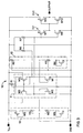
- the reset circuit 10 includes a comparator 11 supplied by a high-potential power rail Vcc and a low-potential power rail GND. An output of the comparator 11 is coupled to node OUTPUT that is linked to reset sub-circuitry of any integrated circuit device requiring power-on reset regulation.
- the reset circuit 10 further includes a first threshold branch 12 and a second threshold branch 13 .
- the first branch 12 includes a first potential drop device 14 and a second potential drop device 15 , wherein a positive terminal of the comparator 11 is coupled to the first branch 12 between the first device 14 and the second device 15 .
- the second branch 13 includes a third potential drop device 16 and a fourth potential drop device 17 , wherein a negative terminal of the comparator is coupled to the second branch 13 between the third device 16 and the fourth device 17 .
- the circuit 10 is designed such that the positive terminal of the comparator 11 defines the reference voltage. When the voltage at the negative terminal exceeds the voltage at the positive terminal, the OUTPUT signal is low. When the positive terminal voltage is greater than that of the negative terminal, OUTPUT is high.
- branches 12 and 13 are both referenced to ground GND potential. As a result, fabrication and temperature changes affect both branches in the same way and are therefore effectively cancelled. In that regard, the comparator 11 continues to compare equivalent differences in the potentials associated with the first branch 12 and the second branch 13 .
- device 15 of branch 12 and device 17 of branch 13 preferably provide substantially equivalent potential drops.
- the device 14 of branch 12 is designed to ensure that the potential at the positive terminal of the comparator 11 is greater than the potential at the negative terminal during the period of time that the potential of Vcc is rising to the required minimum level that triggers switching of the comparator 11 output.
- FIG. 3 presents a preferred design of the circuit 10 described generally with respect to FIG. 2.
- the comparator 11 includes first comparator transistor M0 , second comparator transistor M1 , third comparator transistor M2 , and fourth comparator transistor M3 .
- Transistors M0 and M3 are preferably PMOS transistors with common gates, and transistors M1 and M2 are preferably NMOS transistors.
- the potential drop associated with optional resistive element R1 may also form part of the comparator 11 .
- Branch 12 includes first resistive element R2 , second resistive element R3 , and ground-referencing transistor M4 .
- Branch 13 includes a diode means that is preferably a diode-wired transistor M5 , first resistive element R4 , second resistive element R5 , and ground-referencing transistor M6 .
- Transistor M5 is preferably a PMOS transistor while transistors M4 and M6 are preferably NMOS transistors.
- Resistive elements R1 and R2 each has a high-potential node coupled to high-potential power rail Vcc .
- the low-potential node of R1 is coupled to the source of M0 and the source of M3 of the comparator 11 .
- the gates of M0 and M3 are coupled together and are also coupled to the drain of M0 and the drain of M1 .
- the drain of M3 is coupled to the drain of M2 and the sources of transistors M1 and M2 are both coupled to low-potential power rail GND .
- the drains of transistors M0 and M1 are optionally coupled to Vcc through optional resistive element R6 provide enhanced low- Vcc potential performance, e.g., Vcc ⁇ 0.5V, by charging M0 and M1 under those conditions.
- the gate of transistor M1 is the positive terminal of the comparator 11 . It is coupled to the low-potential node of R2 .
- the gate of transistor M2 is the negative terminal of the comparator 11 . It is coupled to the low-potential node of R4 .
- the drain of M2 is the output of the comparator 11 and is coupled to OUTPUT of the circuit 10 that is couplable to integrated circuitry not shown.
- R2 has its low-potential node coupled to the gate of M1 , as indicated, and to the high-potential node of R3 .
- R3 has its low-potential node coupled to the drain of diode-wired transistor M4 .
- the source of M4 is coupled to GND .
- Diode-wired transistor M5 has its source coupled to Vcc .
- the drain of M5 is coupled to the high-potential node of a voltage divider including resistive elements R4 and R5 .
- the low-potential node of the voltage divider is coupled to the source of diode-wired transistor M6 , which has its gate tied to GND .
- the circuit 10 provides for fabrication- and temperature-independent control of the output of the potential of Vcc on power-up in a tristate configuration as follows. Initially, with Vcc off, all circuit components are essentially at GND potential. As Vcc begins to rise, R2 drives the gate of M1 to a potential substantially equivalent to the potential across R3 and the threshold turn-on voltage drop ( Vt ) across M4 . For the transistors used to form the components of the present invention Vt is generally about 0.7V. At the same time, the output OUTPUT of the circuit tracks Vcc and therefore produces what is the equivalent of a logic high.
- a logic high at OUTPUT blocks the power-on reset of the circuitry to which circuit 10 is coupled.
- the circuit 10 may include resistive element R7 to charge the negative terminal of the comparator 11 at low Vcc potentials, e.g., Vcc ⁇ 0.5V.
- R7 must also be sized to ensure that the branch of comparator 11 including transistor M2 , when on, provides the path of least resistance for transmission of the output signal OUTPUT .
- transistor M5 turns on when Vcc reaches Vt .
- the potential drop across R4 yields a potential at the gate of M2 (the negative terminal of the comparator 11 ) that is less than the potential at the gate of M1 (the positive terminal) and so M2 remains off. Only when the potential of Vcc reaches the equivalent of the Vt of M5 plus the drop across R4 plus the Vt of M2 will M2 turn on. With M2 on, the branch including R1 , M3 , and M2 conducts and the output of the comparator 11 (the drains of transistors M2 and M3 ) is pulled low. For the purpose of the present invention, this will trigger a reset signal corresponding to a Vcc potential equivalent to 2 Vt plus the drop across R4 , which drop can be selected for a desired minimum Vcc power-on value.
- the circuit 10 optionally includes inverter IV1 including CMOS transistors M7 and M8 , and inverter IV2 including CMOS pull-up transistor M9 and pulldown transistor M10 .
- inverter IV1 including CMOS transistors M7 and M8
- inverter IV2 including CMOS pull-up transistor M9 and pulldown transistor M10 .
- less or more inverters may be employed, as well as other sorts of logic functions that will provide the desired output at OUTPUT .
- the elements shown as diode-wired MOS transistors, including transistors M4 , M5 , and M6 may be any sort of diode means including, but not limited to diodes, diode-wired MOS transistors and diode-wired bipolar transistors.
- the design of the circuit described with reference to FIG. 3 provides the advantage of a reduction in the range of Vcc potentials that trigger reset in that it is less fabrication and/or temperature dependent than prior reset circuits. It also provides improved performance in the control of the level of the Vcc potential at which reset will trigger. While reference to the design of FIG. 3 has been made in regard to having transistor M1 on prior to turning on transistor M2 , it is to be understood that the gate couplings for those two transistors may be reversed such that the gate of M1 is coupled to the low-potential node of R4 and the gate of M2 is coupled to the low-potential node of R2 so that the output of the comparator 11 will move from low to high rather than high to low. Of course, in order to complete that transition, the output node OUTPUT would initially have to be tied to GND rather than Vcc .
Landscapes
- Electronic Switches (AREA)
Applications Claiming Priority (2)
| Application Number | Priority Date | Filing Date | Title |
|---|---|---|---|
| US190308 | 1998-11-12 | ||
| US09/190,308 US6160429A (en) | 1998-11-12 | 1998-11-12 | Power-on reset circuit |
Publications (3)
| Publication Number | Publication Date |
|---|---|
| EP1001536A2 true EP1001536A2 (de) | 2000-05-17 |
| EP1001536A3 EP1001536A3 (de) | 2003-07-16 |
| EP1001536B1 EP1001536B1 (de) | 2008-07-16 |
Family
ID=22700806
Family Applications (1)
| Application Number | Title | Priority Date | Filing Date |
|---|---|---|---|
| EP99650097A Expired - Lifetime EP1001536B1 (de) | 1998-11-12 | 1999-10-21 | Einschaltrücksetzschaltung |
Country Status (4)
| Country | Link |
|---|---|
| US (1) | US6160429A (de) |
| EP (1) | EP1001536B1 (de) |
| KR (1) | KR100639759B1 (de) |
| DE (1) | DE69939093D1 (de) |
Cited By (3)
| Publication number | Priority date | Publication date | Assignee | Title |
|---|---|---|---|---|
| EP1501192A1 (de) | 2003-07-21 | 2005-01-26 | Broadcom Corporation | Einschalt- Rücksetzschaltung für niedrige Versorgungsspannungen |
| TWI632773B (zh) * | 2017-09-25 | 2018-08-11 | 立錡科技股份有限公司 | 低耗電電源啟動重設電路與參考訊號電路 |
| CN110971218A (zh) * | 2019-12-18 | 2020-04-07 | 成都海光微电子技术有限公司 | 上电复位电路 |
Families Citing this family (7)
| Publication number | Priority date | Publication date | Assignee | Title |
|---|---|---|---|---|
| US6943596B2 (en) * | 2002-03-12 | 2005-09-13 | Broadcom Corporation | Power-on reset circuit for use in low power supply voltage applications |
| KR100487536B1 (ko) * | 2002-08-20 | 2005-05-03 | 삼성전자주식회사 | 파워-온 리셋 회로 |
| US6998884B2 (en) * | 2003-12-31 | 2006-02-14 | Atmel Corporation | Circuit for auto-clamping input pins to a definite voltage during power-up or reset |
| KR100583611B1 (ko) * | 2005-01-25 | 2006-05-26 | 삼성전자주식회사 | 파워-온 리셋 회로 및 파워-온 리셋 방법 |
| US8872554B2 (en) | 2012-01-06 | 2014-10-28 | Silicon Laboratories Inc. | Externally configurable power-on-reset systems and methods for integrated circuits |
| KR102084547B1 (ko) | 2013-01-18 | 2020-03-05 | 삼성전자주식회사 | 비휘발성 메모리 장치, 그것을 포함하는 메모리 시스템, 및 그것의 외부 전원 제어 방법 |
| JP7251929B2 (ja) * | 2018-06-21 | 2023-04-04 | ラピスセミコンダクタ株式会社 | 半導体装置及びパワーオンリセット信号の生成方法 |
Family Cites Families (7)
| Publication number | Priority date | Publication date | Assignee | Title |
|---|---|---|---|---|
| GB2020437B (en) * | 1978-04-14 | 1982-08-04 | Seiko Instr & Electronics | Voltage detecting circuit |
| US4874965A (en) * | 1987-11-30 | 1989-10-17 | Sgs Microelettronica S.P.A. | Circuital device for the power-on reset of digital integrated circuits in MOS technology |
| US5144159A (en) * | 1990-11-26 | 1992-09-01 | Delco Electronics Corporation | Power-on-reset (POR) circuit having power supply rise time independence |
| JP2761687B2 (ja) * | 1991-12-19 | 1998-06-04 | 三菱電機株式会社 | 電圧レベル検出回路 |
| JP2748950B2 (ja) * | 1991-12-25 | 1998-05-13 | 日本電気株式会社 | パワーオンリセット回路 |
| JP2806783B2 (ja) * | 1994-02-28 | 1998-09-30 | 日本電気株式会社 | パワーオンリセット回路 |
| KR100263924B1 (ko) * | 1997-09-02 | 2000-08-16 | 박태진 | 리셋 신호 발생 장치 |
-
1998
- 1998-11-12 US US09/190,308 patent/US6160429A/en not_active Expired - Lifetime
-
1999
- 1999-10-21 DE DE69939093T patent/DE69939093D1/de not_active Expired - Lifetime
- 1999-10-21 EP EP99650097A patent/EP1001536B1/de not_active Expired - Lifetime
- 1999-10-29 KR KR1019990047353A patent/KR100639759B1/ko not_active Expired - Lifetime
Cited By (4)
| Publication number | Priority date | Publication date | Assignee | Title |
|---|---|---|---|---|
| EP1501192A1 (de) | 2003-07-21 | 2005-01-26 | Broadcom Corporation | Einschalt- Rücksetzschaltung für niedrige Versorgungsspannungen |
| TWI632773B (zh) * | 2017-09-25 | 2018-08-11 | 立錡科技股份有限公司 | 低耗電電源啟動重設電路與參考訊號電路 |
| CN110971218A (zh) * | 2019-12-18 | 2020-04-07 | 成都海光微电子技术有限公司 | 上电复位电路 |
| CN110971218B (zh) * | 2019-12-18 | 2021-04-27 | 成都海光微电子技术有限公司 | 上电复位电路 |
Also Published As
| Publication number | Publication date |
|---|---|
| US6160429A (en) | 2000-12-12 |
| EP1001536B1 (de) | 2008-07-16 |
| DE69939093D1 (de) | 2008-08-28 |
| KR100639759B1 (ko) | 2006-10-27 |
| KR20000035101A (ko) | 2000-06-26 |
| EP1001536A3 (de) | 2003-07-16 |
Similar Documents
| Publication | Publication Date | Title |
|---|---|---|
| EP0692876B1 (de) | Einschaltrücksetzschaltung | |
| US4983857A (en) | Power-up reset circuit | |
| US5144159A (en) | Power-on-reset (POR) circuit having power supply rise time independence | |
| US6914461B2 (en) | Power-on reset circuits including first and second signal generators and related methods | |
| CN102244508B (zh) | 上电复位电路 | |
| US20050140405A1 (en) | Power-up circuit semiconductor memory device | |
| US5767710A (en) | Power-up reset signal generating circuit for an integrated circuit | |
| JP3756961B2 (ja) | 半導体メモリ装置のチップ初期化信号発生回路 | |
| US5883532A (en) | Power-on reset circuit based upon FET threshold level | |
| JP2000165220A (ja) | 起動回路及び半導体集積回路装置 | |
| US20050140404A1 (en) | Power-up circuit in semiconductor memory device | |
| US6160429A (en) | Power-on reset circuit | |
| JP4672126B2 (ja) | 能動アンダシュート強化fetスイッチ | |
| US20080197912A1 (en) | Circuit arrangement for generating a temperature-compensated voltage or current reference value | |
| JP4169288B2 (ja) | 低出力装置用電源投入検出回路 | |
| JP4780840B2 (ja) | 過剰電圧除去検知機能を備えた過剰電圧保護回路 | |
| US6791373B2 (en) | High-voltage detecting circuit | |
| US6760209B1 (en) | Electrostatic discharge protection circuit | |
| JPH0479411A (ja) | パワーオンリセット回路 | |
| US20040217785A1 (en) | Reset circuits | |
| JPH0685648A (ja) | 出力回路 | |
| JP3538480B2 (ja) | 電源切換回路 | |
| US4980792A (en) | BiCMOS power transition circuit | |
| US20020180495A1 (en) | CMOS output circuit | |
| JP3523593B2 (ja) | 改良型パワー・オン・リセット回路 |
Legal Events
| Date | Code | Title | Description |
|---|---|---|---|
| PUAI | Public reference made under article 153(3) epc to a published international application that has entered the european phase |
Free format text: ORIGINAL CODE: 0009012 |
|
| 17P | Request for examination filed |
Effective date: 19991115 |
|
| AK | Designated contracting states |
Kind code of ref document: A2 Designated state(s): AT BE CH CY DE DK ES FI FR GB GR IE IT LI LU MC NL PT SE |
|
| AX | Request for extension of the european patent |
Free format text: AL;LT;LV;MK;RO;SI |
|
| PUAL | Search report despatched |
Free format text: ORIGINAL CODE: 0009013 |
|
| AK | Designated contracting states |
Designated state(s): AT BE CH CY DE DK ES FI FR GB GR IE IT LI LU MC NL PT SE |
|
| AX | Request for extension of the european patent |
Extension state: AL LT LV MK RO SI |
|
| AKX | Designation fees paid |
Designated state(s): DE FR |
|
| 17Q | First examination report despatched |
Effective date: 20060126 |
|
| GRAP | Despatch of communication of intention to grant a patent |
Free format text: ORIGINAL CODE: EPIDOSNIGR1 |
|
| GRAS | Grant fee paid |
Free format text: ORIGINAL CODE: EPIDOSNIGR3 |
|
| GRAA | (expected) grant |
Free format text: ORIGINAL CODE: 0009210 |
|
| AK | Designated contracting states |
Kind code of ref document: B1 Designated state(s): DE FR |
|
| REF | Corresponds to: |
Ref document number: 69939093 Country of ref document: DE Date of ref document: 20080828 Kind code of ref document: P |
|
| PLBE | No opposition filed within time limit |
Free format text: ORIGINAL CODE: 0009261 |
|
| STAA | Information on the status of an ep patent application or granted ep patent |
Free format text: STATUS: NO OPPOSITION FILED WITHIN TIME LIMIT |
|
| 26N | No opposition filed |
Effective date: 20090417 |
|
| PGFP | Annual fee paid to national office [announced via postgrant information from national office to epo] |
Ref country code: FR Payment date: 20101105 Year of fee payment: 12 |
|
| REG | Reference to a national code |
Ref country code: FR Ref legal event code: ST Effective date: 20120629 |
|
| PG25 | Lapsed in a contracting state [announced via postgrant information from national office to epo] |
Ref country code: FR Free format text: LAPSE BECAUSE OF NON-PAYMENT OF DUE FEES Effective date: 20111102 |
|
| PGFP | Annual fee paid to national office [announced via postgrant information from national office to epo] |
Ref country code: DE Payment date: 20180819 Year of fee payment: 20 |
|
| REG | Reference to a national code |
Ref country code: DE Ref legal event code: R071 Ref document number: 69939093 Country of ref document: DE |