EP1001606B1 - Système de commande d'entrée et de sortie d'image - Google Patents
Système de commande d'entrée et de sortie d'image Download PDFInfo
- Publication number
- EP1001606B1 EP1001606B1 EP99308888A EP99308888A EP1001606B1 EP 1001606 B1 EP1001606 B1 EP 1001606B1 EP 99308888 A EP99308888 A EP 99308888A EP 99308888 A EP99308888 A EP 99308888A EP 1001606 B1 EP1001606 B1 EP 1001606B1
- Authority
- EP
- European Patent Office
- Prior art keywords
- bus
- signal
- controller
- data
- transfer
- Prior art date
- Legal status (The legal status is an assumption and is not a legal conclusion. Google has not performed a legal analysis and makes no representation as to the accuracy of the status listed.)
- Expired - Lifetime
Links
- 238000012546 transfer Methods 0.000 claims description 381
- 230000015654 memory Effects 0.000 claims description 222
- 230000001360 synchronised effect Effects 0.000 claims description 63
- 230000006870 function Effects 0.000 claims description 36
- 238000000034 method Methods 0.000 claims description 26
- 230000001419 dependent effect Effects 0.000 claims 1
- 238000010586 diagram Methods 0.000 description 139
- 238000012545 processing Methods 0.000 description 48
- 239000000872 buffer Substances 0.000 description 43
- 239000003795 chemical substances by application Substances 0.000 description 21
- 230000002441 reversible effect Effects 0.000 description 20
- 230000004044 response Effects 0.000 description 17
- 230000007246 mechanism Effects 0.000 description 14
- 230000008569 process Effects 0.000 description 12
- 230000005540 biological transmission Effects 0.000 description 8
- 239000002131 composite material Substances 0.000 description 8
- 239000013256 coordination polymer Substances 0.000 description 8
- 238000012856 packing Methods 0.000 description 8
- 230000002093 peripheral effect Effects 0.000 description 8
- 230000008859 change Effects 0.000 description 5
- 230000003247 decreasing effect Effects 0.000 description 5
- 238000004513 sizing Methods 0.000 description 5
- 238000012986 modification Methods 0.000 description 4
- 230000004048 modification Effects 0.000 description 4
- 238000012544 monitoring process Methods 0.000 description 4
- 238000003860 storage Methods 0.000 description 4
- 230000001629 suppression Effects 0.000 description 4
- 230000009471 action Effects 0.000 description 3
- 238000013479 data entry Methods 0.000 description 3
- 230000000694 effects Effects 0.000 description 3
- 238000013507 mapping Methods 0.000 description 3
- 241001522296 Erithacus rubecula Species 0.000 description 2
- MHABMANUFPZXEB-UHFFFAOYSA-N O-demethyl-aloesaponarin I Natural products O=C1C2=CC=CC(O)=C2C(=O)C2=C1C=C(O)C(C(O)=O)=C2C MHABMANUFPZXEB-UHFFFAOYSA-N 0.000 description 2
- 230000015556 catabolic process Effects 0.000 description 2
- 230000000295 complement effect Effects 0.000 description 2
- 238000012052 concurrent chemoradiation therapy Methods 0.000 description 2
- 238000006731 degradation reaction Methods 0.000 description 2
- 238000005516 engineering process Methods 0.000 description 2
- 239000000203 mixture Substances 0.000 description 2
- 239000002674 ointment Substances 0.000 description 2
- 238000002360 preparation method Methods 0.000 description 2
- 238000007639 printing Methods 0.000 description 2
- 238000006243 chemical reaction Methods 0.000 description 1
- 238000004891 communication Methods 0.000 description 1
- 230000006835 compression Effects 0.000 description 1
- 238000007906 compression Methods 0.000 description 1
- 230000010485 coping Effects 0.000 description 1
- 230000003111 delayed effect Effects 0.000 description 1
- 238000009826 distribution Methods 0.000 description 1
- 230000002708 enhancing effect Effects 0.000 description 1
- 238000007667 floating Methods 0.000 description 1
- 230000002401 inhibitory effect Effects 0.000 description 1
- 230000000873 masking effect Effects 0.000 description 1
- 238000009877 rendering Methods 0.000 description 1
- 238000010187 selection method Methods 0.000 description 1
Images




































Classifications
-
- H—ELECTRICITY
- H04—ELECTRIC COMMUNICATION TECHNIQUE
- H04N—PICTORIAL COMMUNICATION, e.g. TELEVISION
- H04N1/00—Scanning, transmission or reproduction of documents or the like, e.g. facsimile transmission; Details thereof
- H04N1/32—Circuits or arrangements for control or supervision between transmitter and receiver or between image input and image output device, e.g. between a still-image camera and its memory or between a still-image camera and a printer device
- H04N1/32358—Circuits or arrangements for control or supervision between transmitter and receiver or between image input and image output device, e.g. between a still-image camera and its memory or between a still-image camera and a printer device using picture signal storage, e.g. at transmitter
- H04N1/32443—Circuits or arrangements for control or supervision between transmitter and receiver or between image input and image output device, e.g. between a still-image camera and its memory or between a still-image camera and a printer device using picture signal storage, e.g. at transmitter with asynchronous operation of the image input and output devices connected to the memory
-
- H—ELECTRICITY
- H04—ELECTRIC COMMUNICATION TECHNIQUE
- H04N—PICTORIAL COMMUNICATION, e.g. TELEVISION
- H04N1/00—Scanning, transmission or reproduction of documents or the like, e.g. facsimile transmission; Details thereof
- H04N1/00127—Connection or combination of a still picture apparatus with another apparatus, e.g. for storage, processing or transmission of still picture signals or of information associated with a still picture
- H04N1/00204—Connection or combination of a still picture apparatus with another apparatus, e.g. for storage, processing or transmission of still picture signals or of information associated with a still picture with a digital computer or a digital computer system, e.g. an internet server
- H04N1/00236—Connection or combination of a still picture apparatus with another apparatus, e.g. for storage, processing or transmission of still picture signals or of information associated with a still picture with a digital computer or a digital computer system, e.g. an internet server using an image reading or reproducing device, e.g. a facsimile reader or printer, as a local input to or local output from a computer
-
- H—ELECTRICITY
- H04—ELECTRIC COMMUNICATION TECHNIQUE
- H04N—PICTORIAL COMMUNICATION, e.g. TELEVISION
- H04N1/00—Scanning, transmission or reproduction of documents or the like, e.g. facsimile transmission; Details thereof
- H04N1/32—Circuits or arrangements for control or supervision between transmitter and receiver or between image input and image output device, e.g. between a still-image camera and its memory or between a still-image camera and a printer device
- H04N1/32358—Circuits or arrangements for control or supervision between transmitter and receiver or between image input and image output device, e.g. between a still-image camera and its memory or between a still-image camera and a printer device using picture signal storage, e.g. at transmitter
-
- H—ELECTRICITY
- H04—ELECTRIC COMMUNICATION TECHNIQUE
- H04N—PICTORIAL COMMUNICATION, e.g. TELEVISION
- H04N2201/00—Indexing scheme relating to scanning, transmission or reproduction of documents or the like, and to details thereof
- H04N2201/0008—Connection or combination of a still picture apparatus with another apparatus
- H04N2201/0015—Control of image communication with the connected apparatus, e.g. signalling capability
- H04N2201/002—Selecting or switching between an image communication channel and a non-image communication channel
-
- H—ELECTRICITY
- H04—ELECTRIC COMMUNICATION TECHNIQUE
- H04N—PICTORIAL COMMUNICATION, e.g. TELEVISION
- H04N2201/00—Indexing scheme relating to scanning, transmission or reproduction of documents or the like, and to details thereof
- H04N2201/0008—Connection or combination of a still picture apparatus with another apparatus
- H04N2201/0034—Details of the connection, e.g. connector, interface
-
- H—ELECTRICITY
- H04—ELECTRIC COMMUNICATION TECHNIQUE
- H04N—PICTORIAL COMMUNICATION, e.g. TELEVISION
- H04N2201/00—Indexing scheme relating to scanning, transmission or reproduction of documents or the like, and to details thereof
- H04N2201/0077—Types of the still picture apparatus
- H04N2201/0081—Image reader
-
- H—ELECTRICITY
- H04—ELECTRIC COMMUNICATION TECHNIQUE
- H04N—PICTORIAL COMMUNICATION, e.g. TELEVISION
- H04N2201/00—Indexing scheme relating to scanning, transmission or reproduction of documents or the like, and to details thereof
- H04N2201/0077—Types of the still picture apparatus
- H04N2201/0082—Image hardcopy reproducer
Definitions
- the present invention relates to an image input/output control system which effectively controls, for example, an image input apparatus such as a scanner and an image output apparatus such as a printer.
- an image processing system called a composite appliance such as a copying machine or a facsimile which is equipped with a combination of an image input apparatus such as a scanner and an image output apparatus such as a printer as well as a computer system which is equipped with an image input apparatus and an image output apparatus as separate component units.
- a composite function such as a copying function is realized by outputting image data which is taken from the image input apparatus once into a memory to the image output apparatus.
- the composite function such as the copying function is realized by disposing a passage which transfers an image signal from the image input apparatus directly to the image output apparatus.
- the conventional image processing system adopts an optimum circuit configuration dependently on functions of the image input apparatus and the image output apparatus as described above.
- an interface circuit which connects an image input apparatus to an image output apparatus is optimized according to specifications for the image input apparatus and the image output apparatus and specifications for a bus to be connected.
- the configuration of the interface circuit must be modified each time the image input apparatus and the image output apparatus are modified. Accordingly, the conventional image processing system poses a first problem that it does not permit free selection for use of various kinds of image input apparatuses and image output apparatuses.
- the conventional image processing system poses a second problem that it fixes uses of hardware resources such as memories and buses, thereby making it impossible to optimize the hardware resources dependently on various operating modes.
- the conventional image processing system poses a third problem that it requires reserving a memory area even during a copying operation.
- the conventional image processing system poses a fourth problem that a hardware configuration is complicated, thereby constituting a cause to enhance a cost.
- the conventional image processing system poses a fifth problem that it requires modification of the configuration of the interface circuit when the specifications for the image input apparatus and the image output apparatus are changed, when the image input apparatus or the image output apparatus is exchanged or when the specifications for the bus are changed.
- EP-A-0681266 describes an image processing apparatus with a plurality of sections each executing a specified type of processing on the image signal and comparing a controller having a plurality of buses for connecting the sections and selector for bus selection.
- a primary concern of the present invention which has been achieved in view of the conventional example described above is to provide a control system for composite appliances which prepares a plurality of passages as image signal passages corresponding to functions of image input apparatuses and image output apparatuses, and permits selecting an optimum passages out of the image signal passages, thereby requiring no modification of a circuit configuration even when an image input apparatuses and an image output apparatus are changed and permitting freely selecting for use of a various kinds of image input apparatus and image output apparatus.
- a further concern of the present invention is to provide a control system for composite appliances which permits using hardware resources such as memories and buses dependently on various operating modes such as a mode to connect an image input apparatus directly to an image output apparatus, a mode to connect the image input apparatus to the image output apparatus by way of a FIFO and a mode to store image data read from the image input apparatus once into a memory and then output the image data to the image output apparatus.
- a further concern of the present invention is to provide a control system for composite appliances which buffers difference in data rate between an image input apparatus and an image output apparatus with a FIFO when a copying function is realized by outputting a image signal taken from an image input apparatus to an image output apparatus, thereby eliminating the necessity to reserve a memory area for copying.
- a further concern of the present invention is to provide a control system for composite appliances which permits simplifying a hardware configuration regardless of kinds of image input apparatuses and image output apparatuses by preparing a configuration for direct connection of controllers of the image input apparatus and the image output apparatus even when a copying function is realized by providing a passage which connect the image input apparatus directly to the image output apparatus in addition to passages which connect the image input apparatus and the image output apparatus to the memory.
- a further concern of the present invention is to provide a control system for composite appliances which uses a common interface circuit for a bus regardless of specifications for an image input apparatus and an image output apparatus, and comprises a configuration which converts input/output signals from the image input apparatus and the image output apparatus into input/output signals for a bus interface, thereby eliminating a necessity to change a configuration of the interface circuit.
- An image input/output control system comprises:
- the image input/output control system selects one of the three transfer modes dependently on functions of the image signal input means and the image signal output means.
- the image input/output control system selects one of the three transfer modes dependently on whether or not the image signal is to be processed.
- the image input/output control system selects one of the three transfer modes dependently on conditions of use of the memory and buses.
- DoEngine a "DoEngine” preferred as an embodiment of the present invention which is a single-chip scanning and printing engine comprising a processor core, a processor peripheral controller, a memory controller, a scanner/printer controller, a PCI interface and so on.
- the DoEngine is a single-chip scanning printing engine which comprises a processor core compatible with an R4000 Processor manufactured by MIPS Technologies, Inc., a processor peripheral controller, a memory controller, a scanner/printer controller, a PCI interface and so on.
- the DoEngine employs a fast parallel operation and building block techniques.
- the DoEngine Since the DoEngine has the PCI bus interface, it is compatible with a computer system which has a PCI bus slot. Furthermore, the DoEngine has a PCI host bus bridge configuration in addition to a PCI satellite configuration, whereby it can issue a PCI bus configuration, and when it is combined with an inexpensive PCI peripheral device, it is usable as a main engine for a multi-function peripheral. Furthermore, the DoEngine can be combined with a rendering engine having a PCI bus interface and a compression/elongation engine.
- the DoEngine has two independent buses in its chip, namely an IO bus (B bus) which connects universal IO core and a graphics bus (G bus) which is optimized to transfer of image data.
- B bus IO bus
- G bus graphics bus
- High-speed data transfer with high parallelism which is indispensable for simultaneous operations in a multi-function system is realized by connecting a memory and a processor to these buses by way of crossbar switches.
- the memory controller comprises, as a memory, a two way set associative memory front cache having 8 Kbytes to support a synchronous DRAM (SDRAM) which has a maximum cost performance for access to successive data rows represented by image data and minimize performance degradation in random access in a small unit which cannot enjoy a merit of burst access high-speed data transfer from the SDRAM.
- SDRAM synchronous DRAM
- the memory front cache is of a type which hardly allows bus snoop of all memory writes and high performance is obtainable with a cache memory without a complicated mechanism even in a system configuration which adopts a crossbar switch.
- the DoEngine is configured to have a data interface (video interface) between a printer and a scanner which permits real time data transfer (appliance control), and perform high-quality and high-speed copying operation by synchronous support of appliances and image processing with hardware even in a discrete scanner-printer configuration.
- a data interface video interface
- appliance control real time data transfer
- the core operates at 3.3 V and the IO is 5 V tolerant type.
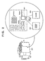
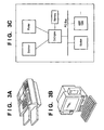
- FIGS. 1 , 2 and 3A through 3C show example of configurations of apparatuses or systems which use DoEngines.
- FIG. 1 shows a discrete type system composed of a personal computer 102 in which a local board 101 comprising a DoEngine is mounted by way of a PCI interface thereof.
- a memory which is connected to the DoEngine by way of a memory bus described later and a color processing circuit (chip) are disposed on the local board 101.
- a high-speed scanner 103 and a color/monochromatic printer 104 are connected to the personal computer 102. Under the control of the personal computer, this configuration makes it possible to process image data input from the scanner 103 with the local board 101 and output the data from the printer 104.
- FIGS. 2 , 3A and 3B shows an example wherein a scanner 203 and a printer 202 are integrally built in: FIG. 2 showing a configuration similar to that of an ordinary copying machine, FIG. 3A showing a configuration of a facsimile or the like.
- FIG. 3B shows a computer which controls the facsimile shown in FIG. 3A .
- FIGS. 1 and 2 show examples of slave mode wherein the DoEngines are controlled by an external CPU connected by way of a PCI interface
- FIGS. 3A and 3B show an example of master mode wherein a CPU of the DoEngine functions as a master unit which controls a device connected by way of a PCI interface.
- the DoEngine is equipped as external interfaces a PCI, a memory bus, a video, general purpose input/output, IEEE 1284, RS232C, 100 base T/10 base T, an LCD panel and keys, and may further have a USB.
- the DoEngine is equipped as built-in blocks a primary cache, a memory controller with cache, a copy engine, an IO bus arbiter (B bus arbiter) a graphics bus arbiter (G bus arbiter) and so on.
- a DMA controller has five channels, and arbitration is performed by arrival order processing with priority for both a graphics bus (G bus) and an IO bus (B bus).
- This section provides a general description of the DoEngine as well as an explanation of a block diagram, an outline, details, a core interface, a timing chart, etc. of each functional block.
- FIG. 4 shows a block diagram of a DoEngine.
- DoEngine 400 has been designed and developed as a main controller for a multi function peripheral (MFP) or a multi function system (MFS) of the next generation.
- MFP multi function peripheral
- MFS multi function system
- MIPS R4000 core manufactured by MIPS Technologies, Inc. is adopted as a CPU (processor core) 401.
- the processor core 401 is connected to a system bus bridge (SBB) 402 by way of a processor bus (SC bus) having 64 bits.
- SBB 402 is a 4 ⁇ 4 crossbar switch having 64 bits, and connected to a memory controller 403 which controls an SDRAM with a cache memory and a ROM by way of an exclusive local bus (MC bus) in addition to the processor core 401, and to a G bus 404 which is a graphics bus and a B bus 405 which is an IO bus: four buses in total.
- the system bus bridge 402 is designed so as to maintain parallel connections among these four modules simultaneously as far as possible.
- the G bus 404 is cooperatively controlled by a G bus arbiter (GBA) 406, and connected to a scanner controller 4302 and a printer controller 4303 for connection to a scanner and a printer.
- BBA B bus arbiter
- the B bus 405 is cooperatively controlled by a B bus arbiter (BBA) 407, and connected not only to a scanner/printer controller but also to a power management unit (PMU) 409, an interrupt controller (IC) 410, a serial interface controller (SIC) 411 which uses a UART, a USB controller 412, a parallel interface controller (PIC) 413 which uses an IEEE1284, an LAN controller (LANC) 414 which uses Ethernet, an LCD panel, a key, a general purpose input/output controller (PC) 415 and a PCI bus interface (PCIC) 416.
- GBA G bus arbiter
- PC general purpose input/output controller
- PCIC PCI bus interface
- Meant by a processor shell is a block which comprises not only a processor core but also an MMU (memory management unit), an instruction cache, a data cache, a writeback buffer and a multiplication unit.
- MMU memory management unit
- a cache memory controller manages three state caches: invalid, valid clean (cache is not updated) and valid dirty (cache is updated). A cache is controlled dependently on this state.
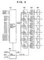
- FIG. 6 shows a block diagram of an interrupt controller 410.
- the interrupt controller 410 is connected to the B bus 405 by way of a B bus interface 605 to collect interrupts from functional blocks in the DoEngine chip and from outside the chip, and relocates them into six levels of external interrupts and non-maskable interrupts (NMI) which are supported by the CPU core 401.
- the functional blocks in the chip are the power management unit 409, the serial interface controller 411, the USB controller 412, the parallel interface controller 413, the Ethernet controller 414, the general purpose IO controller 415, the PCI interface controller 416, a scanner controller 4302, a printer controller 4303 and so on.
- the interrupts can be masked dependently on causes for interrupt with mask registers (Int Mask Logic 0-5) 602 which can be configured as software. Furthermore, an edge sense/level sense is selectable for external interrupt inputs for individual signal lines with a selective edge detector circuit 601. Cause registers (Detect and set Cause Reg 0-5) 603 indicate interrupts which are asserted at each level and is capable of clearing the interrupts by performing write operations.
- mask registers Int Mask Logic 0-5) 602 which can be configured as software.
- an edge sense/level sense is selectable for external interrupt inputs for individual signal lines with a selective edge detector circuit 601.
- Cause registers (Detect and set Cause Reg 0-5) 603 indicate interrupts which are asserted at each level and is capable of clearing the interrupts by performing write operations.
- An interrupt signal at each level is output as a logical sum from a logical sum circuit 604 so that an interrupt signal is output when at least one interrupt is made at each level.
- Leveling among a plurality of causes at each level is made in software.
- FIG. 7 is a block diagram of the memory controller 403.
- the memory controller 403 is connected to an MC bus which is a local bus exclusive for the memory controller by way of an MC bus interface 701, and supports a synchronous DRAM (SDRAM) having a capacity of 1 Gbytes at maximum and a flash ROM or a ROM having a capacity of 32 Mbytes.
- SDRAM synchronous DRAM
- the memory controller performs 64 (16 ⁇ 4) burst transfer in order to make use of a high speed for burst transfer which is obtained as a characteristic of the SDRAM, Taking into consideration single transfer of data having successive addresses from a CPU or a B bus, the memory controller comprises SRAM (memory front cache) 702 to avoid the single transfer directly to the SDRAM as far as possible, thereby enhancing a transfer efficiency.
- a data bus between the memory controller and the SDRAM has a width of 72 bits for a sum of signals ramData and ramPar (8-bit signal ramPar is parity), and data bus between the memory controller and the flash ROM has a width of 32 bits for signals fntromData and prgromData.
- Components of the memory controller are configured as described below:
- the MC bus is provided as a bus exclusively between the SBB 402 and the memory controller 403, and used as a basic bus in the SBB.
- mTType [6:0] is newly defined as a signal representing a burst length.
- MC bus signals are defined as follows:
- This signal is a 32 bit address bus and maintained from a time when mTs_L is asserted until mBRdy_L is asserted.
- This signal is a 64 bit output data bus and is valid only when mDataOe_L is asserted.
- This signal indicates that mDataOut[63:0] is valid. Furthermore, it indicates its transfer is write.
- This signal is a 64 bit input data bus and sampled at rise of mClk for which mBRdy_L is asserted.
- This signal indicates a transfer start. It is asserted during a first clock of transfer. mTs_L is kept asserted when the transfer terminates in a clock and a next transfer starts immediately.
- This signal indicates a transfer type in the MC bus. It is maintained during transfer in single transfer or a first beat in burst transfer.
- Three upper bits represent a source (master) and lower bits designate a single/burst length. Types are listed below: mTType[6:4] Signal source 001 CPU 010 B bus 100 G bus mTType[3:0] Single/burst length 1xxx Single (1-8 byte) 0001 2 bursts 0010 4 bursts 0011 6 bursts 0100 8 bursts 0101 16 bursts 0110 2 ⁇ 16 bursts 0111 3 ⁇ 16 bursts 0000 4 ⁇ 16 bursts
- This signal indicates an effective byte lane in 64 bit data bus in the single transfer. In the burst transfer, this signal is valid for a write time only and ignored for a read time.
- This signal indicates that a current transfer (beat) terminates.
- This signal indicates that a next transfer is write on the same page (the same row address) and that write can be continued up to four at maximum.
- a page size is preliminarily set in a configuration register.
- This signal indicates whether or not an MC bus slave (memory controller) allows in-page write transaction and is sampled by a clock which is the same as that for mBRdy_L.
- mTPW_L is insignificant when mBPWA_L is diasserted.
- This signal asserts when the MC bus slave (memory controller) terminates access while it is not executed and indicates that it must be retried after idling for at least a cycle. (If mBRdy_L and mBRty_L are asserted at the same time, mBRty_L is preferential.)
- This signal is asserted when a parity error or another bus error occurs.
- the SDRAM which has a configuration described below is controlled by the memory controller 403 as described below:
- a DRAM is configured to be capable of performing 8 bank control of a x4, x8, x16 bit type 16/64 megabit SDRAM with 64 bit data bus.
- MA[13: 0] is used in case of a 64 bit SDRAM or MA[11:0] is used in case of a 16 bit SDRAM.
- [Table 3] 64 Mbit SDRAM 31 30 29 ... 27 26 25 24 ... 11 10 ... 3 2 ... 0 0 0 CS C9 C8 R13 ... R0 C7 - C0 BS 16 Mbit SDRAM 31 28 27 ... 25 24 23 22 ... 11 10 ... 3 2 ... 0 0 0 CS C9 C8 R11 ... R0 C7 - C0 BS 0 Zero CS Chip Select C9-CO Column Address C8 is ignored in case of ⁇ 8 bit SDRAM.
- R13-RO Row Address R11 of 16M SDRAM is used to select banks in the SDRAM.
- R12 and R13 are used to select banks in 64M SDRAM which consists of four banks, whereas R13 is used to select banks in 64M SDRAM which consists of two banks.
- SDRAM having programmable configuration (mode register)
- the SDRAM comprises a mode register and sets items mentioned below with mode register setting commands.
- the SDRAM is capable of setting any one of burst lengths of 1, 2, 4, 8 and full page, out of which a burst length of 4 is optimum since a burst transfer length from the CPU is 4. 16 or more bursts can be transferred from the G bus by successively issuing read/write commands (without auto precharge).
- the SDRAM sets an address increment order for burst transfer. It can set "sequential" or "interleave.”
- CAS latency can be set at 1, 2 or 3 which is determined dependently on a grade and of an SDRAM and an operation clock to be used.
- the SDRAM Since the SDRAM operates at 2048 cycles/32 ms (4096/64 ms), it issues a CBR refresh command at intervals of 16, 625 ns.
- the memory controller has a settable refresh counter and automatically issues a CBR refresh command.
- the memory controller does not receive a refresh request during transfer of 16-burst ⁇ n from the G bus. Therefore, the refresh counter must set a value with a margin of a time for the transfer of 16-burst ⁇ 4.
- the memory controller After power on reset, the memory controller initializes the SDRAM as described below. With a pause time of 100 ⁇ s after a power switch is turned on, the memory controller
- the flash ROM controller 704 supports an address signal romAddr[23:2] and four chip select signals (romCs_L[3:0]). Address signals romAddr2-romAddr9 are multiplexed with parity signals ramPar0-ramPar7 and address signals romAddr10-romAddr23 are multiplexed with DRAM addresses ramAddr0-ramAddr13.
- the SDRAM which is used as a main memory provides a remarkably high speed for the burst transfer but cannot exhibit a high speed for the single transfer. Therefore, a memory front cache is mounted in the memory controller to accelerate the single transfer.
- the memory front cache is composed of a cache controller 706 and an SRAM 702. Since transfer masters and transfer lengths of the memory front cache can be known from the mTType[6:0] signal defined by the MC bus, the cache can be set on/off for each master or each transfer length.
- the cache is of types which are listed below. A designation of a cache denotes not a cache built in the processor core, but the memory front cache which is built in the memory controller unless otherwise specified.
- FIG. 8 shows a detailed block diagram of the cache controller 706 and surroundings.
- the DoEngine judges whether the transfer is to be executed with the cache on or off by the mTType[6:0] which is indicated on the MC bus at an initial stage of the transfer. Let us assume in this embodiment that the DoEngine judges cache on for the single transfer and cache off for the burst transfer (step S901). That is, transfer is executed with the cache on when mTType (3) is "1" h indicating the single transfer or with the cache off when mTType(3) is "0" h indicating the burst transfer.
- lmaddr[11:5] is given as an index to b1_tag_ram 801, b2_tag_ram802, b1_data_ram702-a, b2_data_ram 702-b, and lru 803, and a valid bit "v" and b1_tag_addr which correspond to the input indices as well as a valid bit "v,” b2_tag_addr, b1_out_data, b2_out_data and lru_in are output from each block (step S902).
- b1_tag_addr and b2_tag_addr output from the b1_tag_ram 801 and the b2_tag_ram 802 are compared with an address lmaddr[31:12] by a b1_comparator 804 and a b2_comparator 805, whereby hit or miss is informed to the cache controller 706 for judgement by b1_hit_miss_L or b2_hit_miss_L signal (step S903).
- the cache controller 706 judges read or write (step S904).
- Hit means that the b1_tag_addr or b2_tag_addr is coincident with lmaddr [31:12].
- the cache controller 706 judges read or write (step S1001).
- 8-byte data indicated by its lmaddr[31:3] is read out of the SDRAM (step S1003) and output to the MC bus (step S1004).
- lru corresponding to the index is read out and when lru is "0" h, the data from the SDRAM is written into b2_data_ramand lru is also rewritten into "1" h.
- step S1005 When both b1 and b2 are missed and the requested transfer is write, the cache controller 706 only writes the data into the SDRAM to terminate the transfer (step S1002).
- the cache controller 706 reads and writes data from and into the SDRAM only (steps S907 through S909) without rewriting cache data or tag.
- FIG. 11 shows a configuration of a ROM/RAM controller 707.
- Blocks 1101 through 1104 multiplex a data signal, an address signal and a parity signal of the SDRAM into a data signal and an address signal of a flash ROM.
- FIG. 12 shows a timing of burst read from the CPU.
- a burst length is 4 and a CAS latency is 3.
- FIG. 12 corresponds to the processing at the step S909 in FIG. 9 .
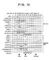
- FIG. 13 shows a timing of burst write from the CPU.
- a burst length is 4 and a CAS latency is 3.
- FIG. 13 corresponds to the processing at the step S908 in FIG. 9 .
- FIG. 14 shows a timing of burst read from the G bus device.
- a burst length of the G bus is 16, a burst length of the SDRAM is 4 and a CAS latency is 3.
- FIG. 14 corresponds to the processing at the step S909 in FIG. 9 .
- FIG. 15 shows a timing of burst write from the G bus device.
- a burst length of the G bus is 16, a burst length of the SDRAM is 4 and a CAS latency is 3.
- FIG. 15 corresponds to the processing at the step S908 in FIG. 9 .
- FIG. 16 a timing of single read when the memory front cache is hit.
- Output as read data mDataIn[63:0] is b1/b2_out_data read out of b1_data_ram 702-a or b2_data_ram 702-b which is a cache memory.
- a burst length of the SDRAM is 4 and a CAS latency is 3.
- FIG. 16 corresponds to the processing at the step S905 in FIG. 9 .
- FIG. 17 shows a timing of single read when the memory front cache is not hit.
- Output as read data mDataIn[63:0] is ramData[63:0] which is read from the SDRAM.
- This data is also written as b1/b2_in_data into b1_data_ram 702-a or b2_data_ram 702-b which is a cache memory.
- a burst length of the SDRAM is 4 and a CAS latency is 3.
- FIG. 17 corresponds to the processing at step S1004 or S1005 in FIG. 10 .
- FIG. 18 shows a timing of single write when the front memory cache is hit.
- Write data mDataOut[63:0] is written into b1_data_ram 702-a or b2_data_ram 702-b which is the cache memory and the SDRAM.
- a burst length of the SDRAM is 4 and a CAS latency is 3.
- FIG. 18 corresponds to the processing at step S906 in FIG. 9 .
- FIG. 19 shows a timing of single write when the memory front cache is not hit.
- the write data mDataOut[63:0] is written not into b1_data_ram 702-a or b2_data_ram 702-b, but only into the SDRAM.
- a burst length of the SDRAM is 4 and a CAS latency is 3.
- FIG. 19 corresponds to the processing at step S1002 in FIG. 10 .
- the memory controller 403 is configured to judge, upon start of the data transfer from the MC bus, the single transfer as cache on or burst transfer as cache off using mTType[6:0] indicated on the MC bus at an initial stage of the data transfer in this embodiment, the memory controller 403 may be configured to further judge a burst length in case of the burst transfer and when the burst length is shorter than a line of the cache, operate with the cache kept on or otherwise operate with the cache kept off.
- the memory controller can judge the identifiers and performs the cache on/cache off control in correspondence to the identifiers. In this case, it is possible to switch cache on/cache off referring to a rewritable table which is prepared to correspond the identifiers to cache on/cache off. When a specific address is allocated to this table, for example, it is rewritable from the CPU 401 or the like.
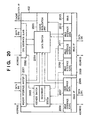
- FIG. 20 shows a block diagram of the system bus bridge (SBB) 402.
- the SBB 402 is a multi-channel two-way bus bridge which provides connections among the B bus (input/output bus), the G bus (graphics bus), the SC bus (processor local bus) and the MC bus with crossbar switches.
- the SBB 402 is capable of establishing two systems at the same time by using crossbar switch, thereby enabling to performs high-speed data transfer with high parallelelism.
- the SBB 402 is equipped with a B bus interface 2906 for connection to the B bus 405, a G bus interface 2006 for connection to the G bus 404, a CPU interface slave port 2002 for connection to the processor core 401 and a memory interface master port for connection to the memory controller 403, and comprises an address switch 2003 for connecting an address bus and a data switch 2004 for connecting a data bus. Furthermore, the SBB 402 is equipped with a cache invalidation unit 2005 which invalidates the cache memory of the processor core.
- a write buffer which accelerates DMA write from the B bus device and read prefetch queues which enhance a read efficiency of the B bus device. Coherency management of data which exists temporarily in these queues is performed by hardware.
- a device which is connected to the B bus is referred to as a device.
- the processor core supports dynamic bus sizing of a 32-bit bus, but the SBB 402 does not support it. This is for the purpose of minimizing a modification of the SBB required in the future to use a processor which does not support the bus sizing.
- FIG. 21 shows a block diagram of the B bus interface.
- the B bus interface 2009 is a two-way bridge circuit between the B bus and the MC bus.
- the B bus is an internal general purpose bus of the DoEngine.
- the B bus interface 2009 comprises five blocks of a master control block 2011, a slave control block 2010, a data interface 2012, a DMAC 2013 and a B bus buffer.
- the DMAC 2013 is functionally divided into three sequencers and a register block. Out of these three sequencers, a DMA memory access sequencer is built in the B bus slave control block 2010 and a DMA reg sequencer is built in the B bus master control block 2011.
- a DMA register which is a register block, is built in the B bus data interface 2012.
- the B bus interface 2009 controls to invalidate two data and instruction caches in the CPU shell by way of a cache invalidation interface when data is written into a memory from the B bus or when data is transferred by the DMA from the device to the memory.
- a writeback buffer at a CPU write time is not mounted in the B bus interface, but a write buffer at external master write on the B bus is mounted. Accordingly, the B bus interface accelerates writes from successive external masters which are not burst transfer. Flash of this write buffer is performed when the memory is allowed to be connected by the B bus arbiter 407. Write buffer bypass of the B bus master read is not made.
- a read prefetch queue of the external master is executed. It is executed to accelerate successive read of data streams from the external master.
- the read buffer is invalidated when:
- each device on the B bus 405 and a DMA controller 2013 between the memories are built in the B bus interface 2009.
- the DMA controller is built in the system bus bridge 402 access requests can be issued simultaneously to both the bridges, thereby performing efficient DMA transfer.
- the B bus interface 2009 does not request use of the dynamic bus sizing in correspondence to an access request from the processor 401.
- the B bus interface 2009 neither responds to bus sizing from the memory controller 403 when the B bus master requests a memory access. That is, the memory controller is not to expect the bus sizing.
- the B bus is a general purpose IO bus in the DoEngine and specified for:
- bus signals are described below in an order of "signal name, input source ⁇ output destination (, 3States) ... description of signal.” An items of 3State is provided only for a signal which has three states.
- a default driver control logic outputs b(Datadrivername) DataOe_L to a device which is granted to output data.
- the b(Datadrivername)DataOe_L signal is returned to the device.
- IOBus Output Control Logic Asserted to IOBus Output Control Logic when the B bus master wants to drive bStart_L,bTx_L,bWr_L,vInstNotData and bAddr[31:2] on a three-state bus.
- the IOBus Output Control Logic returns a b(Mastername)CntlOe_L signal to a master which grants drive on the basis of bMCntlOeReq.
- the B bus slave asserts this signal to indicate that current B bus data transaction terminates with a current clock cycle.
- the B bus master knows by this signal that the current transaction terminates with this clock cycle.
- a B bus slave requests re-execution of bus transaction to the master.
- the B bus slave asserts this signal to IOBus Output Control Logic when it desires to drive bRdy_L,bWBurstReq_L,bBurstAck_L on a 3-state bus.
- the IOBus DefaultDriverLogic returns a b(Slavename)RdyOe_L signal to a slave to which drive is granted on the basis of b(Slavename)RdyOeReq from each master.
- the B bus slave can know the start of the B bus transaction by monitoring this signal.
- the B bus master asserts this signal to the B bus slave to indicate the B bus transaction is currently being executed.
- This signal is driven to indicate that the B bus master executes burst write in response to a B bus burst write request.
- This signal is asserted when the B bus slave requests burst write to the B bus master.
- This signal is asserted to allow the B bus master to inform to the B bus slave that a current transaction is write.
- the B bus signals are defined as described above. Since the B buses (and G buses) which are the internal buses of the DoEngine are to be connected to more than ten functional blocks, it is difficult to connect all the blocks through an InOut separate bus.
- the DoEngine adopts a two-way bus in the chip.
- FIG. 22 shows a block diagram of the G bus interface 2006. it is outlined below.
- the G bus is a bus which is defined to execute high-speed data transfer among image data processing sections in the single chip controller DoEngine for MFPs.
- the G bus has a 64-bit data bus and supports an address space of 4 Gbytes (128-byte boundary).
- a symbol "_L" following a signal name indicates that the signal is low active.
- the G bus signals are described in a manner nearly the same as that for the B bus signals.
- the G bus signals are classified into system signals, address and data signals, interface control signals and arbitration signals.
- a bus agent is a collective name of a bus master and a bus slave which are connected to the bus.
- a signal to indicate that a default driver logic grants data bus drive to a data driver which has output g(DataDrivername)DataOeReq.
- This signal is asserted by the master for one clock to indicates a transfer start (address phase).
- the master drives gAddr,gRdNotWr,gBstCnt together with gTs_L to clarify a kind of the transfer and a data amount.
- the master In case of a write, the master must assure that the clarified transfer data amount can be transmitted with no weight.
- the master In case of a read, the master must assure that the clarified transfer data amount can be received with no weight.
- the slave may cancel transfer of next 16 beats by gBsStep_L. However, the slave never cancels transfer in the course of the 16 beats.
- This signal is driven to Low for a clock by a slave.
- a pertinent slave recognizes transfer, confirms that a bus is empty and informs a master that data transfer can start. In case of a write, the slave must assure that it receives a transfer data amount requested by the master with no weight. In case of a read, the slave must assure that it transmits the requested transfer data amount with no weight. Should data transfer be disabled in the course, next 16-beat transfer can be cancelled by gBstStp_L. However, transfer cannot be cancelled in the course of the 16 beats.
- a request signal for a slave to drive gAack_L A request signal for a slave to drive gAack_L.
- a signal to indicate that a slave is driving to transfer data through a data bus is indicated.
- This signal is driven by a master to indicate READ by High or WRITE byLow. It is driven for the same period as GA.
- This signal is driven by a master to indicate a number (1 to 4) of burst transfers to be executed successively. Values of the signal correspond to numbers of bytes as listed in Table 6.
- This signal is driven by a slave to indicate that next successive burst transfer cannot be received.
- the signal is asserted at 15th beat of 1-burst (16-beat) transfer. It is not driven when it does not stop.
- This signal is driven by a master to request to an arbiter for a bus. It has gReq_L exclusively for each master device.
- This signal is driven by an arbiter to grant a next bus rights for bus requests. It has gGnt_L for each master device. The bus rights are granted in order from bus masters having higher priorities. The bus rights are granted to master having the same priority in order of bus requests.
- This signal is driven by an arbiter to intercept a transaction whose address phase has been started by gGnt_L. However, a transaction whose data phase has been started by gAack_L cannot be intercepted. This signal is masked by gAack_L, thereby being negated and output when gAack_L is asserted.
- the slave When the slave cannot transfer data in an amount requested by the master in the course of the data transfer, it can cancel transfer of next 16 beats by asserting bStStp_L at 15th beat. However, the slave cannot cancel in the course of the 16 beats.
- a cache invalidation unit (hereinafter referred to as CIU in short) 2005 monitors write transaction from the B bus to a memory and when transaction occurs, the cache invalidation unit invalidates a cache built in the CPU shell using a cache invalidation interface of the CPU shell before termination of write into the memory.
- the CPU shell uses three kinds of signals which are mentioned below.
- a cache is invalidated by three clocks at maximum. Since write from the B bus into a memory cannot terminate by three clocks, the cache invalidation unit 2005 does not perform a hand shake of an invalidation end using a stop L signal output from the processor shell 401. However, the cache invalidation unit 2005 drives bSnoop Wait at cycles which are the same as those for Stop_L on the B bus as a preparation for a modification in the future.
- the cache invalidation unit 2005 invalidates also an Icache for security when write occurs from the B bus. Invalidation of the Icache is unnecessary if a self modifying code is inhibited by an OS and the instruction cache is intentionally invalidated for loading data which may be used as an instruction. Some upgrading of performance is expectable in this case.
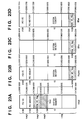
- FIGS. 23A through 23D and FIGS. 24A through 24D show memory maps.
- FIGS. 23A through 23D show a virtual memory map, a physical memory map, a memory map in an address space of the G bus and a memory map in an address space of the B bus respectively.
- FIGS. 24A through 24D are maps which illustrate 512 Mbytes of slashed areas including registers and the like in FIGS. 23A through 23D .
- a memory model of the processor core is based on R3000.
- the processor core has a physical address space of 4 Gbytes by 32-bit addressing.
- a virtual space also performs 32-bit addressing.
- a maximum size of a user process is 2 Gbytes. Address mapping is different between a kernel mode and a user mode.
- the drawings show memory maps where an MMU is not used.
- a user virtual address space (kuseg) of 2 Gbytes are effective for virtual addressing in the user mode. Addresses of the user segments start from 0x00000000 and all effective accesses have msb cleared to 0. Reference to an address at which msb is set in the user mode causes an address error exception processing.
- TLB maps all references to kuseg in the same manner in the user mode and the kernel mode. Furthermore, TLB is cashable. kuseg is ordinarily used to hold the user code and data.
- the virtual address space in the kernel memory mode has four address segments.
- the virtual address space has 4 Gbytes to which access can be made from all memories and I/Os in the system.
- the kseg0 has a built-in RAM (16 MB). When it is desired to program a vector for exception processing, this RAM is implemented and an exception vector base address is set at 0x80000000. This address is mapped at 0x80000000 in the physical address space.
- the kseg1 has ROMs, I/Os and registers which include a boot ROM (16 MB), SBB internal registers, MC internal registers (16 MB) and an IO Bus I/O 1 (16 MB: primitive B bus registers such as a G bus arbiter internal register, a B bus arbiter internal register and a PMU internal register), IO Bus I/O 2 (16 MB), IO Bus MEM (16 MB), G bus MEM (32 MB), FONT ROM (240 MB), FONT ROM or RAM (16 MB).
- the kseg 2 has a PCI I/O (512 MB) and a PCI MEM (512 MB).
- the first 512 Mbytes of all the kseg0, kseg1 and kuseg refer to the same physical address space.
- the physical address space has 4 Gbytes to which access can be made from all the memories and I/Os in the system.
- PCI I/O, PCI MEM and SYSTEM MEMORY are similar to those on the virtual address memory map.
- the G bus address space has 4 Gbytes to which access can be made only from the SYSTEM MEMORY, G bus MEM and FONT.
- the B bus address space has 4 Gbytes to which access can be made only from the PCI, I/O, PCI MEM, SYSTEM MEMORY, IO Bus I/O 2, IO Bus MEM and FONT.
- An address switch 2003 is provided to send an address signal from a bus which is used as a master to a bus which is used as a slave by way of the SBB 402 for data transfer among the SC bus, G bus, B bus and MC bus.
- the SC bus, G bus and B bus can be used as masters, whereas the B bus and MC bus can be used as slaves.
- one of the SC bus, G bus and B bus functions as a master which sends the address signal to the MC bus, whereas only the SC bus functions as a master which sends the address signal to the B bus.
- transfer between the SC bus and the B bus can be executed simultaneously with transfer between the G bus and the MC bus.
- FIG. 25 shows a block diagram of the address switch 2003.
- a switch sequencer 2003a changes over a switch 2003b to select the B bus or the MC bus as a slave and changes over a switch 2003c to select the SC bus, G bus or B bus as a master.
- This configuration uses any one of the SC bus, G bus and B bus as the master for MC bus, selects only the SC bus as the master for the B bus, and allows the transfer between the SC bus and the B bus simultaneously with the transfer between the G bus and the MC bus.
- a data switch functions to switch a data flow in the SBB for data transfer among the SC bus, G bus, B bus and MC bus. Data is sent from a master to a slave for write or from the slave to the master for read.
- FIG. 26 shows a block diagram of a data switch 2004.
- a configuration shown in FIG. 26 is capable of controlling the data flow for write or read by switching selectors A-1 through A-3, B-1 and B-2 as shown in Table 7, thereby selecting the SC bus, G bus or the B bus as a master and setting the B bus or the MC bus as a slave.
- the switch sequencer 2003a disposed in the SBB 402 performs arbitration among three kinds of connection requests from outside the SBB which are listed below:
- the arbitration is determined dependently on current connected conditions of the bus switches and a preliminarily set priority order, thereby changing connections of address switches and data switches.
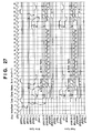
- FIGS. 27 through 32 show timing diagrams.
- FIG. 27 is a timing diagram showing cycles for write/read from the G bus
- FIG. 28 is a timing diagram showing burst stop cycles of the G bus
- FIGS. 29 through 32 are timing diagrams showing transaction stop cycles of the G bus.
- FIG. 33 shows a block diagram of the PCI bus interface 416.
- the PCI bus interface 416 is a block which interfaces the B bus which is an internal general purpose IO bus of the DoEngine with the PCI bus which is an IO bus outside the chip.
- the PCI bus interface 416 can be in a host bridge configuration which is capable of issuing a PCI bus configuration at a reset time or a target configuration which does not issue the PCI bus configuration.
- a master DMA controller 3301 of the B bus interface functions as a B bus master which bridges the access request into the B bus.
- the master DMA controller 3301 is capable of transferring a DMA from a memory mapped in the PCI bus to a DoEngine memory.
- the master DMA controller 3301 issues a transfer destination address (bPciAddr[31:0]) and an ID signal (bPciID) of the PCI master controller 3301 to the B bus and an arbitration sequencer simultaneously with a bus request to operate a B bus DMA intended by a programmer and a G bus DMA in a due access order.
- the master DMA controller 3301 receives a bus grant (bPciBGnt_L) and stops assertion of the ID signal (bPciID) upon completion of the data transfer using a bus.
- PCI bus is rated for 33 MHz, 32 bits and in compliance with PCI 2.1.
- FIG. 34 shows a block diagram of the G bus arbiter (GBA) 406.
- An arbitration of the G bus is of a central arbitration type, and has an exclusive request signal g(mastername)Req_L) and a grant signal (g(mastername)Gnt_L) for each bus master.
- master names are M1 through M4.
- the bus arbiter 406 supports up to 4 bus masters and has characteristics which are described below:
- programming into a register is performed by the CPU 401 by way of the B bus.
- Arbitration sequencers 3402a and 3402b used as kernels of the G bus arbiter perform arbitration between a priority master and other four non-priority masters with five masters.
- the fair arbitration mode is realized by allocating request signals and grant signals from the four bus masters to the four non-priority masters with a request dispatch circuit 3403 and a grant dispatch circuit 3404.
- the G bus arbiter operates in the priority arbitration mode by allocating one of the four bus masters as a priority master of a highly preferential arbitration sequencer 3402a. These allocations are carried out according to setting of registers 3401a and 3401b. Accordingly, the preferential bus master can obtain a right of bus use with a higher possibility than the other masters.
- a master which is allocated to the high priority sequencer 3402a is capable of using the bus successively in a number which is variable with a programmable register. This means that the G bus arbiter is capable of adjusting an occupied ratio of the bus to allow a specific master to use the bus more frequently.
- all the bus masters have the same priority and fair occasions to obtain a bus right.
- a bus master which issues a request first can obtain the bus right.
- the bus right is given sequentially in a predetermined order (round robin mode).
- the bus right is given in an order of M1 ⁇ M2 ⁇ M3 ⁇ M4.
- the bus license is given in a similar order of M1 ⁇ M2 ⁇ M3 ⁇ M4 ⁇ M1 ⁇ M2 ....
- M4 laps round M1 and the bus right is granted to a master whichever has a larger out of those closest to a master which used the bus last.
- a bus master (a bus master registered in the register 3401b) is selected as a priority bus master which has a higher priority than other bus masters and the bus license is given to the priority bus master preferentially to the other bus masters.
- the bus masters other than the priority bus master have the same priority.
- the priority bus master and the other non-priority bus masters obtain the bus license alternately.
- the non-priority bus master cannot obtain the bus license once again only after the bus license is given to all other bus masters which issue requests.
- the priority bus master can obtain the bus license with a transaction stopped so far as a data phase has not been started yet.
- the priority bus master has the bus license immediately before, however, the number of successive obtention of the bus license cannot be exceeded.
- the bus license is given to the bus master preferentially.
- the priority bus master can be switched to another bus master by rewriting the register 3401b.
- the register which selects the priority bus master is rewritten, the priority bus master is switched upon termination of a transaction which is currently executed.
- a state of an arbiter is reset in an idle state and the arbitration is performed once again assuming that a bus master which issued a request at a time of the rewrite issues a request upon termination of the transaction.
- the priority bus master If the priority bus master is switched to a different bus master before a DMA of a bus master which is to have the priority terminates, a priority of a DMA of the initial priority bus master will be lowered. When it is not desired to lower the DMA of the initial priority bus master, the priority bus master must be switched after confirming termination of the DMA.
- the operator should once intercept settings for all the bus masters and the DMA controller to prevent a new DMA request from occurring in the G bus, then set adequate values in the register of the G bus arbiter 406, further check the status register in the G bus arbiter 406 and confirm switching of the priority of the bus master, thereafter making access to a new G bus and starting the DMA.
- Dynamic switching of the priority bus master must be performed with sufficient consideration since it may change or violate real time warranty for an operating system and a setting of task priority.
- FIG. 35 is a block diagram of the G bus 404 and other components in the DoEngine 400 which are related to DMA by the bus masters of the G bus.
- it is considered, for example, to perform processing A of data in a memory 3501 with a bus master 1, perform processing B with a bus master 2 and send processed data to a bus master 4.
- a software for performing these processings i.e., a program to be executed by the CPU 401 sets a sequence to allow the bus masters to use a bus, conditions to start granting the bus license and a condition for end in the register table 3401a in the bus arbiter 406.
- the sequence and the conditions are set as follows: Bus master : Start condition : End condition 1.
- Bus master 1 gM2BufEmpty : gM1BufReady 2.
- Bus master 2 gM1BufReady : gM1BufEmpty 3.
- Bus master 4 gM2BufReady : gM2BufEmpty That is, upon receiving a signal set as the start condition from each bus master, the G bus arbiter 406 grants the bus license to the bus master and upon receiving a signal set as the end condition, the G bus arbiter 406 deprives the bus master of the bus license.
- the software sets a DMA for each bus master.
- each master issues a request (g(mastername)Req_L) to the G bus arbiter 404.
- the G bus arbiter 404 grants the bus right to the bus master 1 in a sequence registered in the register table 3401a (gM1Gnt_L).
- the bus master 1 reads data in a certain unit from a memory 3501, performs the processing A and writes the data into a buffer in the bus master 1.
- the bus master 1 transmits a signal gM1BufReady to the arbiter 406 to inform that the bus master 1 has completed processing of a unit and the buffer is ready.
- the arbiter 406 Upon receiving the signal, the arbiter 406 deprives the bus master 1 of the bus right and grant the bus right to the bus master 2 according to the conditions for granting and depriving of the bus right which are registered in the register table 3401a.
- the bus master 2 reads the data from the buffer of the bus master 1, performs the processing B and stores the data into a buffer in the bus master 2.
- gM1BufEmpty is asserted and the arbiter 406 stops granting the bus right to the bus master 2.
- the bus master 2 performs the processing B and transmits a signal gM2BufReady to inform that its buffer is ready.
- the arbiter 406 receives the signal and grants the bus license to the bus master 4 this time according to contents of the register 3401a.
- the bus master 4 reads the data from the buffer of the bus master 2. When the buffer of the bus master 2 becomes empty, the bus master 4 transmits gM2BufEmpty to the arbiter 406 for information, and the arbiter 406 receives this signal, grants the bus license to the bus master 1 once again according to the contents of the register 3401a and starts a next processing of data.
- each bus master Upon completing the MDA set in each bus master, it causes an interrupt to inform the completion to the processor.
- the software receives end information from all the bus masters, it knows an end of a series of processings.
- a priority sequential mode is prepared. Switching between these modes is performed by programming the register in the arbiter 406.
- the bus masters which perform the sequential processings can preferentially use the bus and the bus masters which are not related to the sequential processings are also allowed to use the bus.
- Arbitration between the bus masters which perform the sequential processings and the bus masters which are not related to the sequential processings is similar to that in the priority arbitration mode which has been described above. It is needless to say that the bus license is not granted to a bus master which is related to the sequential processing but does not satisfy the condition to obtain the bus right and has no turn of itself.
- a scanner controller/printer controller which is one of the G bus masters is excepted from among objects of the arbitration and the bus license is not granted to this G bus master even if it asserts a request.
- the arbitration is performed among the masters, with this G bus excepted. Detailed description will be made separately in a section of B bus arbiter.
- FIG. 36 exemplifies the fair arbitration mode (fair mode) in a case where a number of successive bus use is set at 1 for all the bus masters 1 through 4.
- a second bus request from the bus master 1 (at a timing 4) is postponed until all other bus masters that issues bus requests have been processed once.
- FIG. 37 is an example of fair arbitration mode wherein a number of successive bus use is set at 2 only for the bus master 1 and set at 1 for the other bus masters.
- the second request issued from the bus master 1 (at a timing 4) is granted immediately after a first request and the other bus masters are kept waiting until a processing for the second request has been completed.
- FIG. 38 is an example of priority arbitration mode wherein a number of successive bus use is set at 1 for each bus master and the bus master 1 is set as a priority bus master. Since the bus license is granted alternately to the priority bus master and non-priority bus masters, a second bus request from the bus master 1 is granted after the bus master 2 uses the bus and a bus request from the bus master 4 is granted after the bus master 1 uses the bus for the second time. Furthermore, a second bus request from the bus master 2 is granted after all other bus masters which issue bus request, the bus master 1 and the bus master 4 in FIG. 38 , use the bus.
- FIG. 39 is an example wherein a bus request from the bus master 4 is granted but intercepted by a bus request from the bus master 1. In this case, the bus request from the bus master 4 is granted prior to a bus request from the bus master 2 when the bus master 1 completes use of the bus.
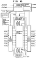
- FIG. 40 is a block diagram of the B bus arbiter 407.
- the B bus arbiter 407 receives a request of bus use from the B bus 405 which is an internal general purpose bus of the DoEngine, gives a license of use to a selected master after arbitration and inhibits the bus from being used by two or more masters at the same time.
- the arbitration mode is configured to have three steps of priorities to each of which a plurality of masters can be allocated programmably. Three masters at maximum can be allocated to a highest priority, seven masters at maximum can be allocated to an intermediate priority and three masters at maximum can be allocated to a lowest priority.
- the B bus arbiter has a mechanism which reserves granting of the right of bus use to a specific master on the basis of the master ID signal and the stop signal from the synchronous unit as a mechanism which functions to maintain an access sequence intended by the user when the G bus master and the B bus master sequentially issue writes to the same address.
- the B bus arbiter is composed of three sequencers 4002, 4003 and 4004. These arbitration sequencers has a high priority, an intermediate priority and a low priority respectively, and comprises arbitration sequencers for three, seven and three bus masters respectively. Request signals from units which may be used as bus masters in the B bus and grant signals to the units are distributed among these three sequencer units by a request selector and a grant selector. This distribution is selectable as a unique combination from among a plurality of combinations by a software-programmable register 4005a in a B bus interface 4005.
- a fair arbitration can be realized, for example, by connecting request from seven masters at maximum to the intermediate priority arbitration sequencer 4003. Furthermore, some of the masters are allocated to the high priority arbitration sequencer 4002 so that they can acquire the bus license at a possibility higher than the other masters. Moreover, some requests are connected to the low priority sequencer 4004 so that they use the bus at a low rate. In addition to adjustment of possibilities to use the bus described above, the masters which are allocated to the high priority sequencer 4002 can use the bus successively in a number which is variable by a programmable register 4005a. Accordingly, the arbitration sequencer can adjust occupied rates of the bus and allow specific masters to use the bus for a longer time.
- the bus license is granted in a similar sequence of M1 ⁇ M2 ⁇ M3 ⁇ M4 ⁇ M5 ⁇ M6 ⁇ M7 ⁇ M1 ⁇ M2.
- the bus license is granted to a master whichever has a largest number closest to that of a master which used the bus last.
- the B bus interface has three arbitration sequencers which have high, intermediate and low priorities.
- An arbitration having a priority order is realized by selectively allocating a plurality of bus requests selectively to high priority and low priority arbiters.
- bus master When a bus master is allocated to the high priority arbiter and rest bus masters are allocated to an intermediate priority arbiter, for example, the bus master functions as a priority bus master having a priority order higher than the rest bus masters and acquires the bus license preferentially to the other bus masters. All bus masters allocated to arbitration sequencers which have the same priority have the same priority order.
- the priority bus master and the other bus masters acquire the bus license alternately.
- M3 is the priority bus master and M1, M2, M3 and M4 issue requests successively, the bus license is granted in a sequence M3 ⁇ M1 ⁇ M3 ⁇ M2 ⁇ M3 ⁇ M4 ⁇ M3 ⁇ M1.
- a high priority bus master can acquire the bus license successively in a number which is preset in a programmable register in an arbiter.
- the number of successive bus use is 4 at maximum.
- the bus master When the bus license is shifted from a bus master other than the priority bus master to another bus master, the bus master cannot acquire the bus license before the bus license is given to all bus masters which issue requests.
- the bus master can acquire the bus license successively if no other bus master issues a request, but only in a preset number if another bus master issues a request.
- the bus master can acquire the bus license once again only after the bus license is granted to all bus masters which issue requests.
- Three requests at maximum can be allocated to the low priority arbitration sequencer 4004.
- the bus license is granted to the bus masters allocated to the low priority sequencer 4004 only in a condition where all the bus masters allocated to the intermediate sequencer and the high priority sequencer do not issue a request. Bus masters must be allocated with sufficient care to the low priority sequencer.
- the priority bus master can be switched by rewriting a register in an arbiter.
- a register which selects the priority bus master is rewritten, the priority bus master is switched upon termination of a transaction which is being executed at that time.
- the arbiter is returned to the idle state and arbitration is performed among bus masters which issued requests when the register is rewritten assuming that the bus masters issue the requests upon termination of the transaction.
- the dynamic switching of the priority bus master must be carried out with sufficient consideration since it may change or violate real time warranty for the operating system and a priority order of tasks.
- the B bus arbiter 407 comprises an access sequence control mechanism.
- the access sequence control mechanism is composed of the synchronous unit 4001, the B bus arbiter 407 and a bus license issuance suppression mechanism built in the G bus arbiter 406.
- a bus license issuance suppression mechanism built in the B bus arbiter 407 operates like that of the G bus arbiter.
- FIG. 41 shows a block diagram of the synchronous unit 4001.
- comparison units 4101 through 4103 are connected to any one of a plurality of combinations of DMA masters.
- the scanner controller/printer controller only exists as a DMA master on the G bus.
- a DMAPCI unit and LAN unit exist on the B bus.
- the B bus interface in the SBB which is a bus master on the B bus does not make access directly to a memory and does not output an ID or a transfer destination address to the synchronous unit 4001.
- FIG. 42 shows a comparison unit 1 out of the comparison units disposed in the synchronous unit.
- the other comparison units have a similar configuration.
- each comparison unit When a request is output from each DMA block, each comparison unit stores the address together with a current time counted with an internal timer, and when an address and a request related to the DMA write are input from another DMA block, each comparison unit compares both the addresses. When the addresses are coincident, the comparison unit further compares the times stored in registers and takes a measure to prevent the bus license from being granted to a bus arbiter of a bus connected to the DMA block which issued the DMA write request at a later time. This measure is informed to a bus arbiter of each bus with a stop (ID) signal.
- ID stop
- Each bus arbiter does not allocate the bus license to the master to which the stop(ID) signal is informed by an arbitration.
- the preceding master dismisses the request from the synchronous unit and the synchronous unit dismisses issuance of the bus license grant inhibiting signal for a DMA block from a bus arbiter of a bus connected to the DMA block which issued the DMA write request secondly. Thereafter, a master which is to perform a DMA write executes the DMA write.
- a timer is reset. The timer counts up once again when a request is output from either of the masters.
- FIG. 43 shows a block diagram of the scanner controller/printer controller and peripheral circuits.
- the scanner/printer controller is a block which interfaces a scanner and a printer with the G bus or the B bus.
- the scanner/printer controller is composed of three functional blocks which are described below:
- a scanner controller is connected to a scanner by way of a video I/F to control operations and data transfer.
- the scanner controller is connected to a G bus/B bus I/F unit 4301A by way of an IF-bus for data transfer and register read/write.
- the data transfer has a master function.
- a printer controller is connected to a printer by way of a video I/F to control operations and data transfer.
- the printer controller is connected to a G bus/B bus I/F unit 4301B by way of an I/F bus for data transfer and register read/write.
- the data transfer has both a master function and a slave function.
- the G bus/B bus I/F units are used to connect the scanner controller 4302 and the printer controller 4303 to the G bus or the B bus.
- the G bus/B bus I/F units are connected independently to the scanner controller 4302 and the printer controller 4303 for connection to the G bus and B bus.
- FIG. 44 shows a block diagram of the scanner controller 4302.
- the scanner controller 4302 is a block which is connected to the scanner by way of a video I/F so as to interface with the G bus/B bus I/F unit (scc GBI) 4301A.
- the scanner controller 4302 is interfaced with the G bus/B bus I/F unit (scc GBI) 4301A by way of an sccI/F bus.
- the scanner controller is composed mostly of blocks which are mentioned below:
- An input/output port to input and output signals into and from the video I/F of the scanner.
- a FIFO which is used when an output destination device may be asynchronous from video data at a stage to output video data from the scanner.
- Kinds of image data input from the scanner include:
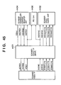
- FIG. 45 shows a block diagram of the scanner device I/F 4401.
- the scanner device I/F is an input/output port which inputs and outputs signals into and from a scanner video I/F 4501 of the scanner unit.
- the scanner device I/F 4401 is capable of determining whether or not level inversion is performed for each of image signals SVideoR [7:0], SVideoG [7:0] and SVideoB [7:0] input from the scanner video I/F in correspondence to a signal VDInvt from the scanner controller control register 4404.
- FIG. 46 shows a block diagram of the scanner video clock unit 4402.
- the scanner video clock unit 4402 is a block which is operated with video clocks from the scanner.
- the scanner video clock unit 4401 is composed of blocks which are mentioned below:
- Masked data has values which are set in a register.
- This control unit manages data numbers and line numbers in horizontal and vertical directions of the image data.
- FIG. 47 shows a block diagram of the scanner video data mask 4601.
- the scanner video data mask 4601 masks the image data input from the scanner in a pixel unit.
- Masked image data has values which are set by a register (RDMask[7:0], GDMask[7:0] and BDMask[7:0]).
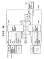
- FIG. 48 shows a block diagram of the scanner video synchronous control unit 4602.
- the scanner video synchronous control unit 4602 generates an enable signal (IVE) for image data to be acquired from a vertical synchronous signal (SVSYNC), a horizontal synchronous signal (SHSYNC) and an image data synchronous clock (GTSVCLK) of image data input from the scanner. Furthermore, the scanner video synchronous control unit 4602 manages a delay in a main scanning direction of the image data, a number of pixels to be acquired, a delay in a subsidiary scanning direction and a number of lines to be acquired. Furthermore, the scanner video synchronous control unit 4602 generates a status signal (PENDP) at a timing when the image data has been acquired in a preset amount.
- PENDP status signal
- a line counter 4801 generates a vertical synchronous signal (EH) for lines effective to read an image by managing the daly in the subsidiary scanning direction and the number of lines to be acquired.
- a pixel counter 4802 manages the image acquistion delay in the main scanning direction and the number of pixels to be acquired.
- a page counter 4803 manages image data to be input in a page unit. It generates an end signal (ALLPEND) when the image data has been input in an amount corresponding to a set number of pages.
- FIG. 49 shows a block diagram of a scanner video data width converter 4603.
- This is a unit which arranges image data input from the scanner in a width of 64 bits. Arranged data is written into the FIFO as 64-bit data. Three kinds of image data, the color image data having 8 bits each in R, G and B, the 8-bit white-black many-valued data and the 1-bit white-black binary data, can be input.
- a mode is set in the scanner controller control register 4404.
- the scanner video data width converter 4603 has a mode in which RGB color image data is arranged in 24 bits in a memory and a mode in which the image data is arranged in 32 bits with an additional byte.
- the three kinds of image data is input from signal lines which are mentioned below:
- the data is rearranged in 64 bits and in the memory as listed below:
- FIG. 54 is a timing diagram of a stage to convert the 8-bit white-black many-valued image data into the 64-bit width by a BW8 packing unit 4901.
- a signal VE is set at a high level
- 8-bit white-black image data R[7:0] from the scanner is acquired and latched pixel by pixel into 64-bit latch in synchronization with signals LP0 through LP7.
- the image data is prepared in an amount of 8 pixels, latched 8 pixels of 64 bits are output as a signal BW8[63:0] in synchronization with a signal LP64.
- FIG. 55 is a timing diagram of a stage to convert the white-black binary image data into the 64-bit width by a shift register 4902.
- binary white-black image data R7 (SVIDEOR0) is acquired in an amount of 64 bits while being shifted bit by bit with the shift register and output as a signal BW1[63:0] in synchronization with a signal SVLATCH64.
- FIG. 56 is a timing chart of a stage to convert the image data having the 8 bits each in R, G and B (24 bits in total) into the 64-bit width with an RGB packing unit 4903.
- FIG. 57 is a block diagram of the RGB packing unit 4903.
- image data R[7:0], G[7:0] and B[7:0] input from the scanner video data mask 4601 is input into 24-bit data latches 5701A and 5701B.
- the data latches 5701A and 5701B latch 24-bit data which are input in synchronization with latch signals LP0 and LP1 having a frequency of a clock CLK divided into halves phases reverse to each other.
- the data latched by the data latches 5701A and 5701B are input into a 48 ⁇ 32 bit data selector 5702 as an input signal RGBHT[47:0] and output as a 32-bit signal DATA[31:0] in correspondence to a 2-bit select signal LP[3:2].
- This signal is output by one of three methods.
- a first method provides an input signal RGBHT[47:16] as the output signal DATA[31:0].
- a second method provides input signals RGBHT[15:0] and RGBHT[47:32] as output signals DATA[31:16] and DATA[15:0] respectively.
- a third method provides an input signal RGNHT[31:0] as the output signal DATA[31:0].
- an output from a data selector 5702 is 24-bit/pixel data summarized in 32 bits. After data from the selector 5702 is selected by the third method described above, however, both data corresponding to two pixels which are input into the data selector must be updated. Accordingly, select signal SELUL[3:2] is delayed for a clock as shown in FIG. 56 .
- the data which has been converted once into the 32-bit width by the data selector 5702 are latched alternately to data latches 5704A and 5704B and contents of the data latch 5704B is output as data converted into the 64-bit width at an updated timing or when a latch signal SELUL1 is set at a high level.
- FIG. 58 shows a block diagram of a scanner image data transfer FIFO controller 4403.
- This block is composed of a FIFO 5801 which is a buffer to transfer image data input from the scanner by way of the G bus or the B bus and a circuit which controls the FIFO 5801.
- This FIFO has a capacity of 512 bytes (64 bits _ 64).
- EF empty flag
- a scanner FIFO write/read arbiter 5802 controls data output from the FIFO.
- Data is input into the FIFO with a request signal (WREQ) from the scanner video clock unit 4402.
- WREQ request signal
- FIG. 59 shows a block diagram of the scanner controller control register 4404. This block comprises registers which control internal members of the scanner controller. Internal registers of this block are:
- FIG. 60 shows a block diagram of an IRQ controller 4406. This block manages an interrupt signal generated in the scanner controller. Interrupt factors are as listed below:
- Flag information (SCIRQ[31:21]) corresponding to the interrupt factors is output to the scanner controller control register 4406.
- a mask bit (SCIMask[31:21]) and a clear signal (SCICLRP[31:21]) corresponding to each interrupt factor are input from the scanner controller control register 4406.
- a logical sum of each interrupt factor is output to the intScc.
- FIG. 61 shows a block diagram of a memory fill mode controller 4405.
- This block controls a mode in which fixed data set in a register is transferred to a memory by way of the GBI. This mode is set with a Memfill signal.
- data MFData[31:0]
- sccWrite a timing signal for data transfer to the sccGBI is generated in this block.
- An sccIF-bus is a local bus which connects the G bus/B bus I/F unit 4301A to the scanner controller 4302.
- This bus comprises signals which are listed below. Signals which are output from the scanner controller to the G bus/B bus I/F unit (GBI) are represented by OUT and signals which are input from the G bus/B bus I/F unit (GBI) to the scanner controller are designated by IN. Since the IF-bus is specified the same for both the scanner controller and the printer controller, signals for functions which are not supported by the scanner controller will also be described. Bclk of the B bus is used as a basic bus.
- This signal is used to return the FIFO in the scanner controller to its initial state.
- GBI G bus/B bus I/F unit
- the G bus/B bus I/F unit acquires sccDataOut[63:0] at rise of Bclk for which the sccWrite signal is asserted. Continuous assertion of the sccWrite signal makes it possible to write data per clock.
- GBI G bus/B bus I/F unit
- GPI G bus/B bus I/F unit
- GBI G bus/B bus I/F unit
- the signal When the signal is "High, " contents of the internal register of the scanner controller are read out to the sccRegDataOut [31:0] and when the signal is "Low,” contents of the sccRegDataIn[31:0] are written into the internal register of the scanner controller.
- the signal becomes valid upon assertion of the sccRegStart_L and is kept valid for the access to the internal register of the scanner controller until response with the sccRegAck_L signal.
- Signals sccRst1_L, scc byte En[7:0], sccRead and sccDataIn[63:0] are contained in the IF bus but not used in the scanner controller.
- FIGS. 62 and 63 are timing diagrams exemplifying timings of the signals which have been described above.
- FIG. 62 shows timings to read data out of the scanner controller 4302 for DMA transfer
- FIG. 63 shows timings to read or write data into or from the internal register of the scanner controller 4302.
- sccPmState[1:0] a PM state signal (sccPmState[1:0]) to be output to a power management unit (PMU) 409 is determined by adding a state of sccDmaPmState[1:0] input from a G bus/B bus I/F unit 4301A to a clock state.
- the sccPmState[1:0] is shown in FIG. 64 .
- the sccDmaPmState[1:0] indicates a power consumption state of a G bus/B bus interface GBI_scc of the scanner.
- the GBI_scc has four power consumption states of 00 to 11.
- the state signal sccDmaPmState[1:0] is output from the GBI_scc to the scanner controller.
- the scanner controller has two consumption states which are indicated by an internal signal SPStat.
- the signal sccPmState[1:0] indicates a total condition consisting of a GBI_scc condition and a scanner controller condition. This signal is output to the power management unit of the system. That is, a power consumption state of the scanner controller is informed at four steps to the power management unit. The steps are indicated by the value of the signal sccPmState[1:0]. A value of 00 indicates a lowest level and each increment of 1 indicates a power consumption at a higher step.
- FIG. 65 summarizes signals which are input and output between core portions including the blocks in the scanner controller 4302 described above and external buses and scanners.
- the scanner controller 4302 is connected to the system bus bridge 402 through the G bus, to the IO devices, power management unit and system bridge through the B bus, to the printer controller through the CP bus, and to the G bus/B bus I/F unit through the I/F bus as shown in FIG. 65 .
- FIG. 66 shows a block diagram of the printer controller 4303.
- the printer controller is a block which is connected to the printer through the video I/F to interface with the G bus/B bus I/F unit.
- the printer controller consists mainly of the blocks which are listed below:
- This unit operates with a video clock of the printer.
- This controller controls an image data transfer FIFO.
- This controller controls an interrupt signal generated in the printer controller (Prc).
- This unit controls transmission and reception of command/status with the printer by way of a video I/F.
- This controller controls a printer option controller.
- This FIFO is used to output video data to the printer when the printer may be asynchronous from the video data.
- FIG. 67 shows a block diagram of a printer device I/F 6601. This block is an input/output port which inputs and outputs signals into and from a printer video I/F and an option controller I/F.
- a signal VDInvet signal can determine whether or not levels of output signals P video R[7:0] and B[7:0] are to be inverted.
- FIG. 68 shows a block diagram of a printer video clock unit 6602. This block operates with a video clock from the printer and is composed of blocks which are described below:
- FIG. 69 shows a block diagram of a printer video data mask 6801. This block masks image data to be output to the printer in a pixel unit. Masked image data has a value set in the register (RDMask[7:0], GDMask[7:0], BDMask[7:0]).
- FIG. 70 shows a block diagram of a printer video synchronous control unit 6802. This block generates an enable signal (VDOEN) for image data to be output and a signal (RREQ) which requests data to the printer image data transfer FIFO controller 6603 with a vertical synchronous signal (TOP), a horizontal synchronous signal (INPHSYNC) and an image data synchronous clock (GTVCLK) for image data to be output to the printer.
- VDOEN enable signal
- RREQ signal
- TOP vertical synchronous signal
- INPHSYNC horizontal synchronous signal
- GTVCLK image data synchronous clock
- this block manages a delay of the image data in a main scanning direction, a number of pixels to be acquired, a delay in a subsidiary scanning direction and a number of lines to be acquired.
- a line counter 7001 generates a status signal (PENDP) at a timing upon termination of output of a set amount of image data.
- the block generates a vertical synchronous signal (EH) for lines effective to output an image by managing the delay in the subsidiary scanning direction and a number of output lines.
- a pixel counter 7002 manages a delay of the image output in the main scanning direction and a number of output pixels.
- a page counter 7003 manages image data to be output in a page unit. It generates an end signal (ALLPEND) upon termination of output of the image data corresponding to a set number of pages.
- FIG. 71 shows a block diagram of a video data width converter 6803.
- This block is a unit which converts data having a width of 64 bits which is input from the GBI (G bus/B Bus I/F) into the format of image data. It can output three types of data: color image data having 8 bits each in R, G and B, 8-bit white-black many-valued image data and 1-bit white-black binary data. It supports outputs in two modes: one wherein the color image data having 8 bits each in R, G and B is stored in a memory in a unit of 24 bits (24-bit mode) and the other wherein the color image data is stored in a unit of 32 bits with 1 byte data added to 24 bits (32-bit mode). Either of the mode is set by the printer controller control register 6604. The three types of data is output to signal lines which are mentioned below:
- 64-bit data is arranged in the memory as described below:
- FIG. 76 shows a block diagram of an RGB out unit 7101. This block is a unit which converts data having a width of 64 bits which is packed in the 24-bit mode into the color image data having 8 bits each in R, G and B.
- FIG. 77 shows a block diagram of a printer image data transfer FIFO controller 6603.
- This controller consists of a FIFO which is a buffer to transfer image data to the printer by way of the GBI (G bus/B bus I/F) and a circuit which controls the FIFO.
- the controller comprises a FIFO 7701 which has a capacity of 512 bytes (64 bits _ 64).
- a printer FIFO write/read arbiter 7702 controls data input into the FIFO while monitoring a full flag (FF) of the FIFO 7701. Data is output to the FIFO when the printer video clock unit 6602 issues a request signal (RREQ).
- FF full flag
- FIG. 78 shows a block diagram of a printer controller control register 6604. This block comprises registers which control internal members of the printer controller.
- the internal registers are:
- FIGS. 79 and 80 show block diagrams of an IRQ controller 6605. This block manages an interrupt signal which is generated in the printer controller. It causes an interrupt from an interrupt factor.
- the IRQ controller has a function to mask each interrupt factor and can clear individually. Interrupt factors are:
- PCIRQ[31:6] corresponding to the interrupt factor mentioned above is output to the printer controller control register 6604.
- a mask bit (PCIMask[31:6]) and a clear signal (PCICLRP[31:6]) corresponding to the interrupt factor are input.
- a logical sum of the interrupt factor is output to intPrc.
- FIG. 81 shows a block diagram of the printer command/status control unit 6606. This is a block which transmits and receives serial commands/statuses for controlling the printer.
- serial commands are an INPCBSY signal which represents a period of command transmission, an INPCCLK signal which is a synchronous clock of the serial command and a serial command INPSRCMD signal.
- an INPSBSY signal whith represents a period of status transmission and a serial status INPSRSTS signal are input to output a 8-bit status PSRSTAT[7:0].
- An INPPCLK signal output from the printer or a PCCLK signal generated by the printer command/status control unit is selectable as a synchronous clock for inputting the serial status. Selection is made by a PSRCLKMode signal.
- FIG. 82 shows a block diagram of the option controller control unit 6607.
- This unit is a block which outputs transmission data (TX) to an option controller. It generates an INSTROBE signal, an INCKEN signal and a CLK(OPCLK) signal for TX transmission. Furthermore, this unit executes reception of reception data (RX) simultaneously with TX transmission.
- a prcIF-bus is a local bus which connects the G bus/B bus I/F unit 4301B to the printer controller 4303. Signals contained in this bus are described below. Signals which are output from the printer controller to the G bus/B bus I/F unit (GBI) are designated by OUT and signals which are input from the G bus/B bus I/F unit (GBI) into the printer controller are designated by IN. Since an IF-bus has specifications which are the same for both the scanner controller and the printer controller, description will be made also of signals for functions which are not supported by the printer controller.
- This signal is used to return an internal FIFO of the printer controller to its initial state.
- GPI G bus/B bus I/F unit
- the G bus/B bus I/F unit (GBI) validates the prcDataIn[63:0]. Data can be read in 1 clock unit by keeping the prcRead signal asserted.
- This signal is output from the G bus/B bus I/F unit (GBI).
- the signal indicates that data can be read at rise of a next clock if the prcReadEnable signal is asserted. Assertion of the prcRead signal is made by confirming the prcReadEnable signal.
- GPI G bus/B bus I/F unit
- This signal becomes valid upon assertion of the prcRegStart_L and is kept valid till response with the prcRegAck_L signal. Only a valid byte indicated by this signal is written into a register. At a stage to read data out of an internal register, this signal is ignored and all bytes are output. Bits of this signal correspond to bytes of prcRegDataIn[31:0] as listed below: sccRegbyteEn: 3 2 1 0 sccRegDataIn: [31:24] [25:16] [15:8] [7:0]
- the signal indicates an access request to the register when it is set at "Low.” It is asserted for 1 clock of Bclk together with the prcRegAddr[31:2] signal and the prcRegRdNotWr signal. Assertion of next access is not granted till the printer controller returns the prcRegAck_L to this access.
- GPI G bus/B bus I/F unit
- Contents of the internal register of the printer controller are read out to the prcRegOut [31:0] when this signal is set at "High” and contents of the prcRegDataIn[31:0] are written into the internal register of the printer controller when the signal is set at "Low.”
- the signal becomes valid upon assertion of prcRegStart_L and is kept valid till response with the prcRegAck_L signal when access is made to the internal register of the printer controller.
- This signal is output from the printer controller to the G bus/B bus I/F unit (GBI). It is asserted for 1 clock of BClk. The signal is sensed at a clock next to assertion of the prcRegStart_L signal.
- FIGS. 83 and 84 are timing diagrams exemplifying timings of the signals described above.
- FIG. 83 shows timings for DMA transfer of data to the printer controller 4303
- FIG. 84 shows timings for read or write from or into the internal register of the printer controller 4303.
- a printer controller In the printer controller, gates of video clocks (VCLK) are controlled according to settings in a printer controller power management control register (0X1B007000), thereby performing power management.
- a value of a PM state signal (prcPmState[1:0]) to be output to the power management unit (PMU) 409 is determined by adding a state of prcDmaPmState[1:0] input from the G bus/B bus I/F unit 4301B to a clock state.
- the prcPmState[1:0] is shown in FIG. 85 .
- the prcDmaPmState[1:0] indicates a power consumption state of a G bus/B bus interface GBI_prc of the printer.
- the GBI_prc has power consumption states at four steps of 00 to 11. This state signal prcDmaPmState[1:0] is output from the GBI_prc to the printer controller.
- the printer controller has power consumption states at two steps which are indicated by an internal signal PPStat.
- the signal prcPmstate[1:0] indicates a state which is composed of a state of the GBI_prc and that of the printer controller. This signal is output to the power management unit of the system. That is, the power consumption states of the printer controller at the four steps are informed to the power management unit.
- the steps are represented by values of the signal prcPmstate [1:0]. A value of 00 represents a lowest level and each increment of 1 designates a higher power consumption.
- FIG. 92 shows a block diagram of the G bus/B bus I/F unit 4301.
- the G bus/B bus I/F unit is prepared for each of the scanner and the printer and has a configuration which is described below:
- the GBI 4301 comprises a G bus controller which is connected to a G bus for its control and a B bus controller which is connected to a B bus for its control.
- a DMA controller 9205 which controls a DMA address
- a FIFO 9204 which is used for data transfer between a functional block and the G bus/B bus
- a register unit 9206 into which various set values are written.
- the G bus controller and the FIFO 9204 operate with clocks at 100 MHz in synchronization with the G bus, whereas other blocks operate at 50 MHz in synchronization with the B bus.
- the GBI 4301 provides selective connection to the G bus or the B bus and a G bus/B bus interface for functional blocks (SCC: scanner controller and PRC: printer controller) which are to be connected to both the G bus and the B bus.
- the GBI is connected to each functional block with an IF bus 9201. It is unnecessary for the functional block to be aware of whether data is to be input or output to the G bus or the B bus. Since DMA is supported by the GBI, it is neither necessary for the functional block to generates an address.
- the GBI is configured as an independent unit by collecting functions which are necessary commonly for the functional blocks.
- a functional block which is connected to the IF bus 9201 supported by the GBI receives or sends out data continuously.
- the IF bus does not contain an address signal.
- the GBI 4301 prepares two channels: channel 0 (G bus/B bus ⁇ IF bus 0) and channel 1 (G bus/B bus ⁇ IF bus 1) to which DMA controllers are prepared respectively.
- the scanner controller uses (mounts) only the channel 0
- the printer controller uses (mounts) only the channel 1.
- a DMA controller 9205 is capable of setting data into an I/O (having fixed address) and a memory, and setting DMA in a continuous physical address mode and a chain table mode (described later) in case of the memory.
- the GBI 4301 inputs and outputs data into and from the functional block by way of the FIFO. Accordingly, an access is made to the same location of an address of the GBI only with 0x18n0_0000 - 0x18n0_007F on a side of the G bus and 0x19n0_0000 - 0x19n0_001F on a side of the B bus when the GBI operates in a slave mode. Since the GBI 4301 uses the FIFO, it can hardly respond to a laparound during burst transfer. The GBI responds to a burst transfer request followed by a laparound of the B bus as a single access. It does not respond to a transfer request which is accompanied by a laparound of the G bus.
- GBI_PRC is selected as a master and GBI_SCC is selected as a slave in this embodiment.
- a GBI (G bus/B bus interface) is composed of:
- the Fifo unit shown in FIG. 93 is a member which functions as a buffer for data transferred between the G bus/B bus and the IF bus.
- the Fifo unit is composed of a FIFO unit 0 and a FIFO unit 1 which are independent of each other.
- the Fifo unit 0 is used to input data from the IF bus or output data to the G bus or the B bus
- the Fifo unit 1 is used to input data from the G bus or the B bus, or output data to the IF bus.
- a signal scGbiFifo0Clk or scGbiFifolClk is a gated clock which realizes a power saving mode by stopping a clock. This clock is stopped by writing a GBI FIFO register and automatically starts when a master mode or a slave mode is to be started.
- the Fifo unit 0 writes data from an IF bus 0 (specifications for the IF bus are described later) into Fifo and sends it to the G bus/B bus. Signals ifDataOutB[63:0], ifWriteB and ifWriteEnableG are connected to the IF bus.
- the Fifo 0 of the Fifo unit 0 receives 64-bit data as an input from the IF bus, and outputs 64-bit data DataOut64 for the G bus and 32-bit data DataOut32 for the B bus.
- a signal Rd64 input into the Fifo 0 is used to read 64-bit G-bus data from the Fifo 0 and a signal Rd32 is used to read 32-bit B-bus data.
- the status signal and DataOut64 or DataOut32 output from the Fifo 0 are updated by reading the 64-bit data or the 32-bit data.
- a B2G block (not shown) which is contained in the Fifo unit 0 converts a clock of a write signal ifWrireFifoB synchronized with the IF bus clock or a read signal bReadFifoB synchronized with the B bus clock into a clock (at a frequency twice as high as that of the IF bus) of the Fifo unit.
- the Fifo 0 is communized by the G bus/B bus.
- the DMA controller controls exclusive use of the G bus/B bus in the master mode, the DMA master must control the exclusive use in the slave mode.
- a ChkIllegal block which is comprised in the Fifo unit 0 asserts a signal fifoErrorG when accesses are made to the Fifo 0 simultaneously from the G bus and the B bus. That is, when a read signal gReadFisoG from the G bus and a read signal bReadFisoB from the B bus are asserted simultaneously, the ChkIllegal block asserts the signal fifoErrorG. This signal is latched by the register unit and causes an interrupt if it is not masked.
- the Fifo unit 1 writes data from the G bus/B bus into a FIFO 1 built therein and sends it out to an IF bus 1. ifDataIng[63:0], ifByteEnG[7:0], ifReadB and ifReadEnableG are connected to the IF bus.
- the Fifo unit 1 comprises a front buffer disposed at its front stage.
- the DMA is in the reverse direction (input signal reverse Mode is enable)
- data is buffered once into the front buffer and then sent out in a reverse sequence to a FIFO.
- signal reverse MODE is disable
- the Fifo unit 1 functions as an ordinary FIFO.
- the front buffer is a buffer having 64 + 4 bits 4 stages with byte enable which receives data from the G bus or the B bus as its input and outputs the data to the Fifo 1.
- the data is written together with a byte enable signal.
- the data is written by validating all byte enables. The data is not packed into 64 bits for write from B bus.
- a status signal is a signal BufEmpty which indicates the front buffer is empty.
- the signal reverseMode is enable and the DMA controller limits a transfer mode only to the 4-beat burst transfer of the G bus or the single transfer of the B bus. Data transferred by the 4-beat burst transfer of the G bus is stored once into the front buffer and sent out to the Fifo 1 in the reverse sequence (reversed in a 32-bit unit).
- the signal reverseMode is disable and the front buffer functions as a FIFO having four stages.
- An input signal dummyWriteFifo1B is once latched and then is sent to the Fifo 1 when the front buffer becomes empty.
- the Fifo 1 is a FIFO having 64 + 8 bits _ 16 stages with a byte enable which receives data from the front buffer as its input and outputs the data to the IF bus.
- Data from the B bus is written together with a byte enable signal.
- Data from the G bus is written with all byte enables validated.
- Data from the B bus is packed into the 64 bits for write.
- the signals Fifo1EnableB1G, Fifo1EnableB4G and Fifo1EnableB8G are used by the DMA controller in the master mode or by the B bus controller in the slave mode.
- the signals Fifo1EnableG4G and Fifo1EnableG16G are used by the DMA controller in the master mode or by the G bus controller in the slave mode.
- the Fifo unit 1 comprises, like the Fifo unit 0, the B2G block and the ChkIllegal block.
- FIG. 94 shows a block diagram of the G bus controller 9202.
- the G bus controller 9202 comprises a G bus master controller which controls the G bus using the GBI as a bus master, a G bus slave controller which controls the G bus when the GBI is selected as a slave, a G bus data controller which controls data and a G bus interface buffer.
- the GBI 4301 is capable of operating as a master or a slave of the G bus.
- the G bus controller which uses a G bus master controller as a G bus master controls the G bus in the processes described below:
- the DMA controller 9205 requests DMA transfer by asserting a gMReq(N) signal together with a gMAddr (N)[31:5] signal and a gMBst4Not16_N signal with bClk (a B bus clock signal) for a clock.
- the gMAddr (N)[31:5] signal and the gMBst4Not16_N signal must not be changed until any of gMDone (N) signal, gMRtry(N) signal and gMBErr(N) signal is asserted by the G bus master controller.
- a gMReq (N) signal is latched by a G bus master request interface (gLatchReq(N) signal).
- a gLatchReq signal in each channel which is arbitrated by a G bus master request arbiter (not shown) asserts a DMA request signal gReq_L for the G bus arbiter 406 and transmits a gIntReq(N) signal to a G bus master address phase.
- a gGnt_L signal which is a DMA grant signal from the G bus arbiter 406 is asserted
- a signal GGntSense is asserted and the DMArequest signal gReq_L is negated from the G bus master address phase.
- the gLatchReq (N) signal and the gIntReq (N) signal are negated.
- the G bus master request interface monitors a signal gSlvBsy and asserts a GMDataRq(N) signal when a data bus becomes usable. This signal is sent to G bus master generate end data and a G bus data controller.
- the G bus starts data transfer when it confirms the gAack signal of a slave.
- G bus signals other than EndData are generated by the G bus master address phase.
- the EndData is generated G bus by master generate end data.
- Data is moved from the G bus to the Fifo or from the Fifo to the G bus by the G bus data controller with a GMDataRq (N) signal.
- N GMDataRq
- the G bus master generate end data informs an end of the G bus data transfer to the G bus master request interface with a checkBErr signal. Upon reception of this signal, the G bus master request interface clears a request held therein and asserts the gMDone signal if no bus error is made. When a bus error is detected, the G bus master request interface asserts the gMBErr signal to inform the end of transfer to the DMA controller 9205.
- the G bus master reqeust interface clear the request held therein and asserts the gMRtry signal.
- the DMA controller 9205 updates a transfer address, a transfer length and so on.
- the received signal is the gMRtry signal
- the DMA controller does not update the transfer address, etc., but starts a next action.
- the DMA controller 9205 intercepts the transfer and generates an interrupt if it is not masked.
- the G bus controller which uses a G bus slave controller as a G bus slave controls in the processes described below:
- a G bus slave request interface confirms a gAddrReg signal and a gRdNotWrReg signal (channel 0 or 1) at a timing to assert a gTsReg signal. If a gSEnable(N) signal (slave mode: set by a register) is asserted by an access to the GBI, the G bus slave request interface judges whether or not transfer is possible from a gBst4Not16 signal and a ReadFifoEnable4/16 signal (channel 0) or a WriteFifoEnable4/16 signal (channel 1). If possible, the G bus slave request interface asserts the gAack signal or otherwise, it asserts the gRtry signal.
- a gSEnable(N) signal slave mode: set by a register
- the G bus slave request interface When data transfer is enabled, the G bus slave request interface confirms negation of the gSlvBsy signal, asserts the gAack signal and informs its timing to G bus slave request slave busy with the GSlvStart signal. Furthermore, the G bus slave request interface informs a start of data transfer to the G bus data controller by asserting the GSDataRq (N) signal. The G bus data controller moves data from the G bus to the Fifo or from the Fifo to the G bus. The G bus slave request slave busy generates a gSlvBsy signal.
- No signal is prepared in particular to indicate a transfer end.
- the gBErr signal is not asserted.
- the gSEnable (N) signal has been negated, however, a bus error occurs due to time-out since no response is made to an access from the master.
- FIG. 95 shows a block diagram of the B bus controller 9203.
- the B bus controller 9203 comprises a B bus master controller, a B bus data controller, a B bus slave controller and a B bus interface buffer. This configuration allows the GBI 4301 to operate as a master or a slave of the B bus.
- the DMA controller 9205 When data transfer through the channel N becomes possible, the DMA controller 9205 asserts a bMReq (N) signal together with a bMAddr(N)[31:2] signal, bMBurst8n) signal and bMBstNot8_N signal for a clock with a B bus clock signal bCLk. Furthermore, at a stage to require read of a chain table in a chain DMA mode, the DMA controller 9205 asserts a cMReq(N) signal together with a cMAddr(N)[31:2] signal with the bClk for a clock. The DMA controller 9205 does not use B bus burst transfer to read the chain table. DMA transfer of the B bus is required from the DMA controller through these processes.
- the bMAddr(N)[31:2] signal, bMBurst(N) signal and bMBst4Not8_N signal must not be chaged until access to the Fifo is started (bReadFifo and bWrireFifo are asserted).
- the cMAddr(N) [31:2] signal must not either be changed until the cMDone(N) signal, cMrtry(N) signal or cMBErr(N) signal is asserted.
- the BBusbMReq(N) signal and cMReq(N) signal are latched by the B bus master request interface (bLatchReq (N) signal and cLatchReq(N) signal).
- BBLatchReq (N) signal and cLatchReq(N) signal Each request signal is arbitrated by the B bus master request arbiter and a bBReq_L signal is asserted for the B bus arbiter 407.
- a B bus master request arbiter When the bBGnt_L signal which is a grant signal from the B bus arbiter is asserted, a B bus master request arbiter transmits a BGnt(N) signal or a CGnt(N) signal to a B bus master request interface which is a corresponding request source to negate a bBGnt_L signal.
- the B bus master request interface negates the bLatchReq(N) signal or the cLatchReq (N) signal, monitors a bTx signal and a bSnoopWait signal, and asserts a BMDataRq (N) signal and a CMDataRq (N) signal when a state is that transfer is possible. These signals are sent to the B bus master sequencer and the B bus data controller.
- a B bus master sequencer generates all B bus signals other than data to be driven by the B bus master.
- the B bus master sequencer triggers the BMDataRq (N) signal or the CMDataRq(N) signal, asserts bStartOut_L (and bBurstOut_L at the same time in the burst mode) and checks bRdy (or bBurstAck in the burst mode), thereby detecting a transfer end.
- the B bus data controller transfers data from the B bus to the Fifo or from the Fifo to the B bus with the BMDataRq(N) signal.
- the B bus data controller When the bRretry signal is detected before (or simultaneously with) the bRdy signal, the B bus data controller does not transfer data.
- the B bus data controller terminates the data transfer by a BMLastData signal from the B bus master sequencer. Furthermore, the B bus master sequencer informs the data transfer end to the B bus request interface with a Done signal. In case of a retry or a bus error, the B bus master sequencer informs with a retry signal or an Error signal.
- the B bus master request interface informs the transfer end, retry or bus error to the DMA controller with [bc] MDone (N) signal (either b or c will hereinafter be represented as [bc]), a [bc]MRtry (N) signal or a [bc]MBErr signal respectively.
- the DMA controller updates a transfer address, a transfer length and so on with signals bReadFifo and bWriteFifo, and starts a next action with a bMDone (N) signal or a bMRtry(N) signal which indicates a DMA B bus transfer end.
- a cMDone(N) signal which indicates readend of the chain table updates an internal chain table and issues a transfer request once again with the cMRtry(N) signal.
- the DMA controller intercepts the transfer and generates an interrupt if it is not masked.
- the slave When the slave responds by asserting the signal bRdy_L and the signal bBurstAck_L at the same time without asserting the signal bRetry_L to simultaneous assertion of the signal bStart_L and the signal bBurst_L, the slave is judged as ready for a burst transfer.
- the signal bRetry_L is not checked. In other words, the signal bRetry_L is checked only at a timing of a first bRdy_L. Even during the burst transfer, the signal bError_L is checked at every clock.
- the signal byteEn_L[3:0] is always set at "0000" except for last transfer for the single access or the burst access.
- the B bus master sequencer confirms the bAddr and bWr_L signals (channel 0 or 1) at a timing of assertion of the bStart_L signal.
- a bSEnable(N) signal is asserted (slave mode: set by a register) for access to the GBI
- the B bus master sequencer judges whether or not transfer is possible from a bBurstShortNotLong signal (only when the bBurst_L signal is asserted) and a ReadFifoEnablel/4/8 signal (channel 0) or a WriteFifoEnable1/4/8 signal (channel 1).
- the B bus master sequencer asserts the bRdyOut_L signal (and the bBusrtAckOut_L signal in the burst mode) or otherwise, it asserts the bRetryOut_L signal.
- the burst transfer is impossible due to a Fifo state but the single transfer is possible in correspondence to the burst mode request (assertion of the bBurst_L signal) from the master, only the bRdyOut_L signal is asserted and the single transfer is executed.
- the burst mode request from the master generates a lap around, the GBI does not correspond the lap around and the single transfer is executed if possible (the bBurstAckOut_L signal is not asserted).
- the B bus master sequencer asserts the bRdyOut_L signal continuously for a required number of clocks. In case of the burst transfer, it asserts the bBurstAckOut_L signal for a B bus clock at a timing of assertion of a first bRdyOut_L signal.
- the B bus master sequencer informs a data transfer start and a data transfer end to the B bus data controller with a BSDataRq(N) signal and a bMLastData signal respectively.
- the B bus data controller transfers data from the B bus to the Fifo or from the Fifo to the B bus.
- No signal is prepared in particular to indicate a transfer end. Either, the bErrorOut_L signal is not asserted. When the bSEnable(N) signal is negated, however, the B bus master sequencer does not respond to access and a bus error is generated due to time-out.
- Accesses to the GBI and registers in the functional blocks are made from the B bus.
- An access to the register can be made at any time regardless of a mode or a status of the GBI. It is unnecessary to assert the bRetryOut_L signal or the bErrorOut_L signal.
- the B bus slave sequencer always responds with the single transfer to a request of the burst mode request from a master (does not assert the bBurstAckOut_L signal).
- the register controller 9206 senses the regStart_L, regAddr[31:2], byteEnIn[3:0] and regWr_L signals (B bus signals tapped by the B bus clock), writes data of the bDataIn[31:0] signal when data is to be written into a register and asserts an Ack signal (regGbiAck_L in the GBI or regIfAck_L in the IF bus).
- the B bus slave sequencer When data is to be read out from a register, the B bus slave sequencer set data in an internal bus (regGbiDataOut[31:0] in the GBI or regIfDataOut[31:0] in the IF bus) and asserts an Ack signal (regGbiAck_L in the GBI or reglfAck_L in the IF bus).
- the Bbus slave sequencer generates bRdyOut_L from the Ack signal with a B bus slave generate ready block.
- a cycle for the single transfer is always 3B bus clock.
- the burst transfer asserts a first bRdyOut_L signal at a timing which is the same as that for the single transfer and keeps it asserted for a required number of clocks without negating the signal.
- transfer single transfer and burst transfer
- it asserts only bRetryOut_L at a timing to assert the first bRdyOut_L.
- the B bus slave generate ready block ORs and taps with clocks a ChannelRdy_L signal from the B bus slave sequencer, a regGbiAck_L signal from the GBI register unit and a regIfAck_L signal from the functional block (IF bus).
- An IF bus is a simple bus which connects the GBI to the functional block. It uses a clock of bClk (50 MHz).
- An input signal means herein a signal sent in a direction from the functional block to the GBI. No two-way signal is used.
- IF bus signals will be described below.
- a suffix "_L" of a signal name represents low active. This suffix is used commonly to the signal names which have already been described above. In practical implementation "if" in the signal names is to be replaced with a name of a functional block.
- the signal is asserted by an internal register of the GBI. It is always asserted prior to data transfer between the GBI and the functional block.
- the GBI writes ifDataOut[63:0] at rise of ifClk for which the ifWrite signal is asserted. Data can be written in a 1 clock unit when ifWrireB signal is asserted continuously. This signal is connected to the Fifo unit 0 (see FIG. 93 ).
- the ifWriteEnableG signal which is asserted at rise of ifClk indicates that write is possible at rise of a next clock.
- An ifWriteB signal is asserted by confirming the ifWriteEnableG signal. This signal is output from the Fifo unit 0.
- This signal is a data signal or a byte enable signal from the GBI to the functional block. This signal is connected to the Fifo unit 1. Correspondence between each digit of the ifByteEnG[7:0] signal and each byte unit of the ifDataInG[63:0] signal is listed in Table 8: [Table 8] ifByteEn 7 6 5 4 3 2 1 0 ifDataIn 63:56 55:48 47:40 39:32 31:24 23:16 15:8 7:0
- the GBI outputs ifDataInG[63:0] andifByteEnG[7:0] at rise of ifClk for which the ifRead signal is asserted. Continuous assertion of the ifRead signal makes it possible to read data in the 1 clock unit. This signal is connected to the Fifo unit 1.
- the ifReadEnableG signal which is asserted at rise of ifClk indicates that read is possible at rise of a next clock.
- the ifRead signal is asserted by confirming the ifReadEnableG signal. This signal is output from the Fifo unit 1.
- This signal is validated upon assertion of the signal ifRegStart_L and is kept valid during response with the ifRegAck_L signal when an access is made to an internal register of the functional block. In case of write into the internal register of the functional block, only an effective byte which is indicated by this signal is written. In case of read from the internal register of the functional block, this signal is ignored and all bytes are output. This signal is output from the B bus controller.
- Table 9 lists correspondence between each digit of the signal ifRegByteEn[3:0] and each byte unit of the signal ifRegDataInG[31:0]: [Table 9] ifRegByteEn 3 2 1 0 ifRegDataIn 31:24 23:16 15:8 7:0
- contents of the internal register of the functional block are output to the signal ifReqDataOut [31:0] and when the signal is low, data of the ifReqDataIn[31:0] is written into the internal register of the functional block.
- the signal becomes valid upon assertion of the signal ifRegStart_L and is kept valid till response with the ifRegAck_L signal when an access is made to the internal register of the functional block. This signal is output from the B bus controller.
- the functional block generates a power management status signal to the power management unit on the basis of this signal and an operating state of the functional block itself. This signal is output from the register unit. A value to be output will be described later in a section of a power management.
- the GBI uses DMA controllers 9205 shown in FIG. 96 in channels 0 and 1 respectively.
- the DMA controller consists of a DMA main controller block, a fetch chain table block, a calculate pitch address block, a generate address block and a DMA request block.
- Mode signal modeMem useChainTable reverseMode Chain table DMA I 1 0 Chain table DMA (Reverse direction) 1 Continuous address DMA 1 0 0 Continuous address DMA (Reverse direction) 1 To I/O DMA 0 0 always 0
- a chain table type DMA starts the fetch chain table block, the generate address block and the DMA request block in this order at intervals of 1 clock.
- a DMA with a pitch starts the calculate pitch address block, the generate address block and the DMA request block in this order at intervals of 1 clock.
- Another type of DMA starts the generate address block and the DMA request block at an interval of 1 clock.
- the DMA main controller judges a DMA end.
- the DMA main controller asserts a stopDMAReq signal for each block when it detects assertion of a NextAddreReq signal for the generate address block (a length counter is zeroed), a bus error or assertion of a stopDMA signal (forcible DMA end by a register) in an idle state of the fetch chain table block (the block has read all contents of the chain table or is not started) and in an idle state of the calculate pitch address block (the block has completed all lines or is not started).
- the DMA main controller judges the DMA end (asserts endDMa) when all the blocks are set in idle states.
- the fetch chain table block fetches tables in memories and is not started when a chain table is not used.
- the fetch chain table block consists of a chain table pointer address counter which designates a chain table for memory address, a chain table entry counter which indicates a number of rest entries in the chain table, a next address register which stores an address and a length fetched from the chain table, a next length register and a fetch chain table controller which controls the counters and the registers mentioned above.
- the fetch chain table After the next address register is latched, the fetch chain table requests fetch of an address of the chainAddress[31:2] to the B bus controller. With the chainDone signal, the read contents are latched to a next length address to increase the chain table pointer address counter and decrease the chain table entry counter. Simultaneously, the fetch chain table asserts a nextAddrValid signal and informs to the generate address block that an address and a length have been read from the chain table.
- the fetch chain table judges that the generate address block has received the address and the length from the chain table, and negates the nextAddrValid signal.
- the fetch chain table checks the chain table entry counter and continues the fetch of chain table once again when the counter is not zero or returns to an idle state when the counter is zero.
- the fetch chain table Upon receiving a chainBErr signal (bus error), the fetch chain table returns immediately to the idle state.
- the fetch chain table receives stopDMAReq from the DMA main controller, the fetch chain table returns to the idle state after an end of a request if it issues a request to the B bus main controller or otherwise, it immediately returns to the idle state.
- the fetch chain table is not started or is kept in the idle state and the nextAddrValid signal is kept negated.
- the generate address block comprises a transfer memory address counter to store a transfer address to a memory, a transfer length counter to store a transfer length to be transferred, a transfer counter to store a byte which has been transferred, a generate address controller to control these three counters, and a CheckGBusReq block and a CheckBBusReq block (referred to collectively as a CheckG/BBusReq) which judge a mode to be requested to the GBus/Bus from a transfer address and a transfer length.
- a transfer memory address counter to store a transfer address to a memory
- a transfer length counter to store a transfer length to be transferred
- a transfer counter to store a byte which has been transferred
- a generate address controller to control these three counters
- a CheckGBusReq block and a CheckBBusReq block (referred to collectively as a CheckG/BBusReq) which judge a mode to be requested to the GBus/Bus from a transfer address and a transfer length.
- the chain table When the chain table is started from the DMA main controller, it clears the transfer counter and waits for a nextValidAddrCT signal from the fetch chain table. When the nextValidAddrCT signal is asserted, an address and a length of the chain table are loaded into the transfer memory address counter and the transfer length counter respectively.
- the CheckG/BBusReq judges a mode selectable for transfer from contents of the two counters.
- the CheckG/BBusReq informs a transfer mode of the G/BBus to the DMA request block (a g/b Valid signal is negated when transfer is impossible) and the DMA request block issues a transfer request to each bus controller while giving a priority to the G bus.
- the transfer memory address counter and the transfer counter are increased and transfer length counter is decreased at a time by a gMDone signal (transfer end signal through G bus) and a selected transfer mode.
- the transfer memory address counter is increased and the transfer length counter is decreased.
- the fetch chain table When the transfer length counter is zeroed upon completing transfer of a final portion of the chain table, the fetch chain table is in an idle state and the nextValidAddrCT signal is negated. Since the DMA main controller detects an end of the DMA, it asserts the stopDMAReq signal for the generate address block. The generate address block is set in the idle state accordingly.
- the generate address block When the generate address block is started from the DMA main controller, it clears the transfer counter and waits for a nextValidAddrPA signal from a calculate pitch address. When the nextValidAddrPA signal is asserted, an address and a length calculated from a start address and a pitch are loaded into the transfer memory address counter and the transfer length counter respectively.
- the transfer memory address counter and the transfer counter are increased and the transfer length counter is decreased.
- the calculate pitch address is in an idle state and the nextValidAddrPA signal is negated. Since the DMA main controller detects an end of the DMA, it asserts the stopDMAReq signal for the generate address block. The generate address block is set in the idle state accordingly.
- the transfer counter is cleared and contents of a GBIDMA transfer length register which stores a data length are loaded into the transfer length counter.
- the CheckGBusReq block and the CheckBBusReq block use contents of GBIDMAGBus I/O address register and GBIDMABBus I/O register respectively.
- the transfer counter is increased and the transfer length counter is decreased as described above.
- the fetch chain table and the calculate pitch address which were not started are in idle states, and the nextValidAddr signal is negated. Since the DMA main controller detects an end of the DMA, it asserts the stopDMAReq signal for the generate address block. The generate address block is set in an idle state accordingly.
- the generate address block supports a reverse mode when it does not operate for DMA to I/O. It makes accesses to a block of the chain table DMA and a line of the DMA with pitch in order from higher to lower addresses.
- chain tables are prepared in the reverse direction in the chain table DMA.
- a value of the pitch is set as a negative value (a complementary number of 2).
- a final address is calculated using a transfer length to load a value into the transfer memory address counter.
- the transfer memory address counter is not increased but decreased.
- the CheckBBusReq block requests the single transfer only.
- the CheckGBusReq block requests the 4-beat burst transfer only. Data is set in a reverse sequence in a 32-bit unit by the Fifo unit and sent to the functional block (responding only to the channel 1 in present conditions).
- the CheckGBusReq block checks the GBus request.
- the signal gValid is always negated unless a signal useGBus is active.
- the signal gValid is negated in other cases.
- the CheckBBusReq block checks the BBus request.
- the signal bValid is always negated unless the signal useBBus is active.
- the DMA request block checks a request for the G bus/B bus from the generate address block.
- the generate address block issues requests for both the G bus and the B bus, the G bus is used preferentially.
- the DMA request block issues a transfer request to the G bus controller or the B bus controller and waits for a response.
- the response is a signal of g/bMDone, g/bMRtry or g/bMBErr.
- the DMA request block checks a next GBus/BBus request from the generate address block.
- the generate address block issues a transfer request once again to the same bus controller.
- the DMA request block is set in a state to wait for a GBus/BBus request from the generate address block. Since the DMA main controller detects an end of the DMA and issues stopDMAReq signal in response to a DMA request, DMARequest is returned to an idle state by this signal.
- the DMA main controller In case of a bus error at a time of the chain table fetch or a forcible end of the DMA by a register, the DMA main controller also issues the stopDMAReq signal and the DMARequest returns to the idle state after completion of transfer when a transfer request is issued to the bus controller, or otherwise, the DMARequest returns to the idle state immediately.
- Register units corresponding to individual channels exist in the internal register. These register units are the same, except for addresses to be decoded.
- the register unit comprises a register unit 0 and a register unit 1 as shown in FIG. 97 .
- Each register unit is composed of a register I/F block, an action controller block, an interrupt controller block and a power status block.
- the register unit supplies a set point value to each block of the GBI and controls not only an interrupt with an interrupt controller but also blocks which can operate in a power saving mode with a power status block.
- Units of the GBI which can operate in the power saving mode are the DMA controller and the FIFO unit.
- the power saving mode is realized by masking a clock of each block with a fifoInSleep signal and a dmaInSleep signal. Both the units are set in the power saving mode when they are reset.
- the DMA controller automatically starts when initiated in the master mode and enters into sleep with write of a GBIFIFO sleep register.
- Power management status signals (pmState[1:0]) which are output from the power status block to the channels are: pmState[1:0] 00 level0 (both DMA and FIFO stopped) 01 level1 (only FIFO operates) 10 level2 (both DMA and FIFO operate) 11 NotDefine
- the power management signals are prepared as listed above for the GBI of the DoEngine which is connected to the scanner controller (Scc) and the printer controller (Prc) has only the channel 1, but when it includes two channels, the signals are degenerated to 4 stages as shown below: pmState[1:0] 00 level0 (both DMA and FIFO stopped) pmState[1:0] 00 level0 (both FIFO and DMA stopped in both channels) 01 level1 (FIFO operates only in channel 1) 10 level2 (FIFOs operate in both channels but DMAs stopped in both channels) 11 level3 (FIFOs operate in both channels and a DMA operates)
- the power management status signal (pmState[1:0]) is sent to the functional block by way of the IF bus. On the basis of this signal and an operating status of the functional block itself, the functional block generates a power management status signal to the power management unit.
- the GBI operates in DMA modes which are listed below:
- the GBI transfers data to:
- the DMA to the continuous physical addresses is the so-called two-dimensional DMA in which a head address, a length of a line, a pitch to a next line and a number of lines are designated.
- a one-dimensional DMA can be realized by setting the number of lines at 1.
- a head address and a length of each divided memory block are disposed in a memory, and an address of a transfer destination is calculated while referring to the head address and the length to execute the DMA.
- a pair of the head address and the length will hereinafter be referred to as a chain table.
- FIG. 98 exemplifies a chain table.
- a memory address in which the chain table is disposed and a number of address-length pairs are designated.
- the chain table itself must be arranged at continuous addresses needless to say, it is possible to connect chain tables by setting a length of 0 for an address of a next chain table in place of a head address when all chain tables cannot be arranged at continuous areas.
- a chain table is prepared in the reverse direction.
- a pitch value is set as a negative value (a complementary number of 2).
- the DMA is ended normally when transfer requested by the DMA controller to a bus controller terminates normally.
- the DMA is ended abnormally due to the bus error.
- the DMA is ended (an interrupt occurs) when the functional block has written all data into the FIFO in the GBI but data remains in the FIFO. Since the DMA is ended when FIFO data is transferred, the GBI judges the transfer of the FIFO data as an end of the DMA.
- the GBI ends the DMA (causes an interrupt) when all data has been written into the FIFO but data remains in the FIFO. Since the functional block is ended when the FIFO data is transferred, the GBI judges the transfer of the FIFO data as an end.
- Data is transferred between the functional block and a master which are connected to the GBI by way of the FIFO of the GBI.
- both the G bus and the B bus are used (in the DoEngine, the GBI is a unique master which is capable of using both the G bus and the B bus) and both the buses issue access request simultaneously, there is no available method to know which of the buses will make access first to the FIFO.
- the master must issue an exclusive transfer request to the G bus/B bus. (The GBI issues an exclusive transfer request in the master mode.) If both the G bus and B bus make accesses to the FIFO simultaneously, a FIFO illegal access occurs.
- An interrupt is caused when any one of the conditions 1 through 5 mentioned above occurs and the interrupt grant bit is set at "1.”
- FIG. 99 shows a diagram of a core interface which is composed of a combination of the interfaces between the GBI and the B bus/G bus/functional block. Since the GBI does not issue the bus error during the B bus slave operation, it is free from bError(Func)Out_L. Furthermore, the GBI does not check the bInstNotData signal during the B bus slave operation, it is free from (func) bInstNotData in and (func) bInstNotData_out always drive "0.”
- the GBI does not issue the bus error during the G bus slave operation, it is free from (func) gErr_L_out.
- a functional block to be connected that is, scc (scanner controller) or prc (printer controller) is set as Func (func) in the signal name of the GBI shown in FIG. 99 .
- the DoEngine uses the scanner controller Scc (scc) and the printer controller Prc (prc) as functional blocks. Since data flow is not in two directions when either of the functional blocks is used, the DoEngine is implemented with unnecessary FIFOs, DMA controllers and registers omitted.
- FIG. 86 is a diagram showing a collection of signals which are input and output between cores including the blocks described above in the printer controller 4303 and external buses and scanners.
- the printer controller 4303 is connected to the system bus bridge 402 by way of the G bus, to the IO device, power management device and system bus bridge by way of the B bus, to the printer controller by way of the PC bus and to the G bus/B bus I/F unit by way of the I/F bus.
- FIG. 87 shows a block diagram of the power management unit 409.
- the DoEngine is a large-scale ASIC which comprises the CPU. It is therefore fearful that a large amount of heat is generated and the chip itself may be broken when all internal logic operate at the same time. In order to prevent such a trouble, the DoEngine manages electric power supplied to each block or perform power management and monitors an amount of electric power consumed by the chip as a whole.
- the power management is performed independently by each block.
- Data of an amount of electric power consumed by each block is collected to the power management unit (PMU) 409 as a power management level.
- the PMU 409 totalizes amounts of electric power consumed by the blocks and monitors the amounts of electric power consumed by the blocks of the DoEngine so that a total value will not exceed a limit of electric power consumption.
- the power management unit operates as described below:
- the level configuration and power consumption values are held in the PM component register 5401.
- Power management may be optionally configured independently for each block. Examples of power management configuration will be described below:
- FIG. 88 shows a block diagram of a bus agent.
- the power management unit 409 manages the consumed power so that it will not exceeds a predetermined value.
- the system which has the configuration described above is capable of transferring image data read from the scanner directly to the printer and carrying out a copying operation to form an image with the printer.
- the scanner/printer system which uses the DoEngine preferred as the embodiment is capable of selecting three kinds of copying mode dependently on system configurations which are described below:
- a first mode is selectable by a system which has a configuration wherein vertical and horizontal timings for image input by the scanner are coincident with horizontal and vertical timings for image output from the printer respectively, and a transfer speed of video data is also coincident.
- a vertical synchronous signal is output from the printer and input into the printer controller (PRC).
- This VSYNC signal is input from the printer controller (PRC) to the scanner controller (SCC) by way of the CP bus.
- the signal is output from the scanner controller (SCC) to the scanner.
- the printer is vertically synchronized with the scanner accordingly.
- a horizontal synchronous signal (HSYNC) signal is output, like the vertical synchronous signal VSYNC, from the printer and input into the scanner by way of the printer controller, CP-bus and the scanner controller.
- the scanner is horizontally synchronized with the printer accordingly.
- the scanner and the printer operate in synchronization in the vertical and horizontal directions as described above.
- the video data is output together with a synchronous video clock from the scanner.
- the output video clock and video data are input into the scanner controller (SCC) and then input into the printer controller (PRC) by way of the CP bus.
- the clock and data are output from the printer (PRC) controller to the printer.
- the printer receives the video data in synchronization with the video clock and outputs an image.
- This copying operation is carried out by a configuration shown in FIG. 89 . This copying operation is carried out without using the G bus or the B bus.
- the image data is transferred from the scanner directly to the printer by way of the CP bus during this copying operation, the image data can simultaneously be written into a SDRAM by the DMA transfer of the G bus from the scanner controller (SCC).
- the image data which is written into the SDRAM during the copying operation can be stored as image data as occasion demands.
- the image data read by the scanner can be output to a plurality of members without operating the scanner.
- a second mode is selectable by a system which has a configuration wherein a horizontal timing for image input by the scanner is coincident with a horizontal timing for image output from the printer but a vertical timing is not coincident with a video data transfer speed.
- a copying operation in this mode will be described with reference to FIG. 90 .
- the scanner controller SCC
- three timing signals of a vertical synchronous signal (VSYNC), a horizontal synchronous signal (HSYNC) and a video clock are input into the scanner controller (SCC).
- video data is also input into the scanner controller (SCC).
- the scanner controller SCC acquires the video data into an internal FIFO (FIFO_SCC). Simultaneously with image data entry into the FIFO_SCC, it starts data transfer to a FIFO (FIFO_GBI_SCC) of the G bus/B bus I/F unit 4301A (GBI_SCC) of the scanner.
- FIFO_GBI_SCC FIFO_GBI_SCC
- the image data is sequentially transferred from the scanner to the FIFO_GBI_SCC by way of the FIFO_SCC.
- the DMA transfer is started using the G bus/B bus I/F unit 4301B (GBI_PRC) of the printer as a master and the G bus/B bus I/F unit 4301A (GBI_SCC)of the scanner as a slave.
- G bus is used when it is empty but the B bus may be used when the G bus is not empty.
- the image data of the FIFO_SCC is transferred to the FIFO (FIFO_GBI_PRC) in GBI_PRC.
- the image data of the FIFO_GBI_PRC is sequentially transferred to the FIFO (FIFO_PRC) of the printer controller (PRC).
- the printer controller (PRC) Upon image data entry into the FIFO_PRC, the printer controller (PRC) inputs the vertical synchronous signal (VSYNC) into the printer.
- the printer starts outputting the horizontal synchronous signal (HSYNC) and the video clock with the timing of VSYNC.
- the printer controller (PRC) synchronizes the video data with the horizontal synchronous signal HSYNC and output the video data from the FIFO_PRC in synchronization with the video clock.
- the video data is output from the printer as an image.
- the image is copied by transferring the image data in a sequence of the scanner, the FIFO (FIFO_SCC) of the scanner controller, the FIFO (FIFO_GBI_SCC) of the G bus/B bus I/F unit, the FIFO (FIFO_GBI_PRC) of the G bus/B bus I/F unit, the FIFO (FIFO_PRC) of the printer controller and the printer. Since intervals of the horizontal synchronization is the same between the scanner and the printer, a difference of the image data transfer speed is buffered by each FIFO.
- a third mode is selected by the system which has a configuration wherein a vertical synchronous timing, a horizontal synchronous timing and a video data transfer speed are different from one another between the scanner and the printer.
- a copying operation in this mode will be described with reference to FIG. 91 .
- the scanner When the scanner starts reading an image, the scanner outputs a vertical synchronous signal (VSYNC), a horizontal synchronous signal (HSYNC) and a video clock to the scanner controller (SCC). Image data is output in synchronization with these timing signals.
- the scanner controller (SCC) acquires the image data in synchronization with the timing signals mentioned above.
- the GBI_SCC performs the DMA transfer of acquired image data to the memory controller (MC) 403.
- the image data transferred by DMA is written by the MC403 into the SDRAM.
- an amount of the image data written into the SDRAM reaches to a level sufficient to buffer a difference between the data transfer speeds of the scanner and the printer, image data transfer to the printer is started.
- the amount of the image data can be judged from a data transfer time from the scanner, an address written into the SDRAM, an amount of data transferred by DMA to the GBI_SCC or the like.
- the printer controller (PRC) transfers the image data to the printer.
- the printer controller (PRC) inputs the image data written in the SDRAM sequentially into the internal FIFO.
- the printer controller (PRC) outputs the vertical synchronous signal (VSYNC) to the printer.
- the horizontal synchronous signal (HSYNC) and the video clock are input from the printer.
- the printer controller outputs the image data from the internal FIFO to the printer.
- a copying operation is carried out to output the image data read by the scanner from the printer.
- the image data flows in a sequence of the scanner, scanner controller, G bus/B bus I/F unit (GBI_SCC) of the scanner, memory controller (MC), SDRAM, memory controller (MC), G bus/B bus I/F unit (GBI_PRC) of the printer, printer controller (PRC) and printer.
- the copying operation is carried out by storing the image data once into the memory and transferring the image data from the scanner to the printer using the memory as a buffer between the scanner and the printer as described above.
- the system has functions for the copying operation in three modes described above.
- a larger number of the internal blocks which are used for the copying operation is increased in an order of (mode 1) ⁇ (mode 2) ⁇ (mode 3).
- Use of a larger number of the internal blocks constitutes a cause for degradation of performance or an efficiency of the system as a whole.
- the system permits selecting a copying operation mode where the system operates most efficiently dependently on a number of devices (the printer and scanner) which are connected to the system.
- the coping operation modes can be selected, for example, by methods which are described below:
- a copying operation mode which is determined or selected by the methods (1) through (3) is informed from the CPU to the printer controller and the scanner controller so that the printer controller, the scanner controller and the like carry out the copying operation.
- FIG. 100 is a flowchart showing processes to select a copying mode to be used by the system out of the three copying operation mode. This operation starts at a step S1 at a rise time of a power source of the system.
- a type of the printer is judged.
- the CPU 401 acquires an ID from the printer through a command/status line included in the printer video I/F.
- the command/status line is a serial communication line which is capable of communicating command/status 1:1 between the printer controller and the printer.
- the CPU similarly acquires an ID indicating a type from the scanner though a command/status line included in the scanner video I/F by way of the scanner controller 4302.
- a copy passage suited to a combination of the scanner and the printer which is judged at the steps S2 and S3 is judged.
- Judgement of the copy passage suited to the combination of the scanner and the printer is prepared in a form of a table, for example, in a memory of a flash ROM to which the CPU can make reference.
- a combinations of the scanner and the printer which is suited for each copy passage is:
- the CPU selects an adequate copying operation mode from among the three modes mentioned above by referring to a prepared table.
- a mode corresponding to the copying operation mode selected at the step S4 is set for the scanner controller 4302.
- the CPU sets this mode by way of the B bus.
- FIG. 101 is a diagram showing a circuit which switches the internal data bus of the scanner controller 4302.
- a data bus selector is included in the scanner device I/F 4401 shown in FIG. 44 .
- the scanner video clock unit and other members which are not necessary for description of data bus switching are omitted.
- a data bus mode is set in a register 1.
- a mode which corresponds to a copying operation mode selected at the step S4 in FIG. 100 is set in a register 1 by the CPU.
- a select control signal 4 is a signal used to select a data bus in correspondence to the mode which is set in the mode setting register 1.
- a scanner video bus 2 is a video data bus from the scanner.
- a bus 5 is used to transfer video data from the scanner to the FIFO_SCC 6.
- a CP video bus 7 is used for the copying operation in the (mode 1).
- a data bus is selected so that video data is output from the scanner video bus to the CP video bus 7.
- the video data is output to the bus 5 and transferred to the FIFO_SCC 4407.
- the CPU proceeds to a step S6 in FIG. 100 .
- the system sets an operation mode for the GBI_scc. This mode is set in the copying operation mode which is selected by the CPU at the step S4.
- the GBI_scc is designated so as not to operate.
- a master is designated for the DMA transfer and the GBI_prc is set in a transfer destination of the DMA.
- the (mode 3) a master is designated for the DMA transfer and the SDRAM is set in the transfer destination of the DMA.
- an operation mode is set for the GBI_prc. This mode is set by the CPU in the copying operation mode selected at the step S4.
- the GBI_prc is designated so as not to operate.
- a slave is designated for the DMA transfer.
- a master is designated for the DMA transfer and the SDRAM is set in a read source for the DMA transfer.
- a mode is set for the printer controller. This mode is set by the CPU in the copying operation mode selected at the step S4.
- FIG. 102 is a diagram showing a circuit which switches the internal data bus of the printer controller 4303.
- a data bus mode is set in a register 11.
- a mode which corresponds to the copying operation mode selected at the step S4 in FIG. 100 is set in the register 11 by the CPU.
- a select control signal 14 is used to select a data bus according to the mode set in the mode setting register 11.
- a bus 15 is a bus for data output from the FIFO_PRC 16.
- a bus 12 is a video data bus to the printer.
- a CP video bus 17 is used for the copying operation in the (mode 1). In case of the (mode 1) , data in the CP video bus is selected and output to the printer. In case of the (mode 2) or (mode 3), data from the bus 15 is output to the printer video bus 12.
- a flow to select a copying operation mode terminates at rise of the power source.
- the CPU is capable of determining a copying operation mode dependently on types of the scanner and the printer.
- the processes described above are those for determining a copying operation mode on the basis of the vertical synchronization timing, horizontal synchronization timing and video data transfer speeds of the scanner and the printer, but not always applicable to a case where an image is to be not only copied but also to be processed.
- Speaking concretely of a case where an image is to be processed it is judged whether or not the image is to be processed before the step S2 in FIG. 100 and the mode 3 is selected regardless of specifications for the scanner and the printer and each block is set to obtain the data passage in the mode 3 at the steps S5 through S8.
- These processes allow read image data to be stored once into a memory, thereby making it possible to process the image data as required.
- a bus is used in the mode 2 or the mode 3.
- the system determines whether the G bus or the B bus is to be used dependently on their conditions of use. In other words, the G bus which has a broader width is used when both the G bus and the B bus are in the idle states. When either of the buses is not used, the system selects the other bus which is not used.
- the scanner is connected to the buses (G bus and B bus) in the DoEngine by way of the scanner controller 4302 and the GBI_SCC 4301A.
- the scanner controller 3402 and the GBI_SCC 4301A are connected to transfer image data to each other by way of the FIFOs respectively. Since the scanner controller and the GBI_SCC have the FIFOs respectively as described above, the GBI is capable of efficiently transferring image data read from the scanner which has a relatively low speed though the operation clock is connected at the 64-bit width to the G bus which has a remarkably high speed of 100 MHz.
- the printer controller is also capable of efficiently transferring the image data.
- the GBI selects a data passage for the copying operation dependently on coincidence or mismatching between the synchronous signals of the scanner and the printer, thereby being capable of copying an image using data transfer as speedy as possible regardless of specifications for the scanner and the printer.
- connections of the scanner and the printer to the buses of the DoEngine using the scanner controller and the printer controller described above as well as their GBIs make it possible to make the DoEngine mode independent from the specifications for the scanner and the printer.
- the operating sequence of the cache shown in FIGS. 9 and 10 may be those shown in FIGS. 103 and 104 .
- the memory controller checks the mTType[3:0] at the start of the transfer and operates with the cache on when a burst length indicated by the mTType is 1/2/4 or operates with the cache off when the burst length is 6/8/16/2 ⁇ 16/3 ⁇ 16/4 ⁇ 16. After the cache is turned on or off, the memory controller operates as shown in FIGS. 9 and 10 .
- the cache can be turned on and off with a device as shown in FIGS. 105 and 106 .
- the memory controller discriminates a device which issues a transfer request by checking the mTType[6:4] at a transfer start, refers to a value of a component register which is preliminarily set to judge whether it operates with the cache on or off, and determines whether it operates with the cache on or off.
- the memory controller operates as shown in FIGS. 9 and 10 .
- Setting of the component register may be determined (not modifiable) by a hardware or rewritten by a software.
- the image input/output control system is capable of preparing a plurality of passages as passages for image signals dependently on functions of an image input apparatus and an image output apparatus, and selecting a most adequate passage out of the plurality of passages, thereby not requiting a circuit composition even when the image input apparatus and the image output apparatus are changed and being capable of freely selecting various kinds of image input apparatuses and image output apparatuses.
- the image input/output control system is usable in various operation modes including a mode wherein hardware resources such as a memory and a bus are connected directly to an image input apparatus and an image output apparatus, and another mode wherein the hardware resources are connected by way of FIFOs.
- the image input/output control system makes it unnecessary to reserve a memory area for copying by using the FIFO to buffer a difference in data rates between the image input apparatus and the image output apparatus.
- the image input/output control system is capable of simplifying a hardware configuration by preparing members which directly connect controllers of the image input apparatus and the image output apparatus regardless of specifications for the image input apparatus and the image output apparatus.
- the image input/output control system does not require modifying a composition of an interface circuit since it uses a common interface circuit with buses regardless of the specifications for the image input apparatus and the image output apparatus, and has the configuration to convert input and output signals from the image input apparatus and the image output apparatus into input and output signals for a bus interface.
- the image input/output control system has enhanced independence and can cope with more flexibly to specifications for a printer and a scanner connected to the system since it permits a passage optimum for image data to be copied and connects controllers of the scanner and the printer to bus interface with data transfer between FIFOs.
Landscapes
- Engineering & Computer Science (AREA)
- Multimedia (AREA)
- Signal Processing (AREA)
- General Engineering & Computer Science (AREA)
- Computing Systems (AREA)
- Image Input (AREA)
- Facsimiles In General (AREA)
- Bus Control (AREA)
- Information Transfer Systems (AREA)
Claims (6)
- Système de commande d'entrée/sortie d'images (400) comprenant :une pluralité de bus (404, 405) ;une unité de commande d'entrée (4302) pour fournir en entrée un signal d'image provenant d'un moyen d'entrée de signal d'image (103) ;une première interface de bus (4301A) pour connecter ladite unité de commande d'entrée à au moins l'un de ladite pluralité de bus ;une unité de commande de sortie (4303) pour fournir en sortie le signal d'image au moyen de sortie de signal d'image (104) ;une deuxième interface de bus (4301B) pour connecter ladite unité de commande de sortie à au moins l'un de ladite pluralité de bus ;une mémoire (403) à laquelle un accès peut être fait à partir de chacun de ladite pluralité de bus ; etun bus de commande (CP-Bus) destiné à connecter directement et exclusivement ladite unité de commande d'entrée (4302) à ladite unité de commande de sortie (4303) ;caractérisé en ce que le signal d'image est transféré dudit moyen d'entrée de signal d'image (103) audit moyen de sortie de signal d'image (104) dans un premier mode de transfert dans lequel le signal d'image est directement transféré de ladite unité de commande d'entrée (4302) à ladite unité de commande de sortie (4303) via ledit bus de commande (CP-Bus), dans un deuxième mode de transfert dans lequel le signal d'image est transféré de ladite première interface de bus (4301A) à ladite deuxième interface de bus (4301B) via ladite pluralité de bus, ou dans un troisième mode de transfert dans lequel le signal d'image est transféré de ladite première interface de bus (4301A) à ladite mémoire (403) et le signal d'image est transféré de ladite mémoire à ladite deuxième interface de bus (4301B) via l'un de ladite pluralité de bus.
- Système de commande d'entrée/sortie d'image selon la revendication 1, dans lequel l'un desdits trois modes de transfert est sélectionné d'une façon qui dépend de fonctions dudit moyen d'entrée de signal d'image et dudit moyen de sortie de signal d'image.
- Système de commande d'entrée/sortie d'image selon la revendication 1, dans lequel l'un desdits trois modes de transfert est sélectionné d'une façon qui dépend du fait que ledit signal d'image doit ou non être traité.
- Système de commande d'entrée/sortie d'image selon la revendication 1, dans lequel l'un desdits trois modes de transfert est sélectionné d'une façon qui dépend des conditions d'utilisation de ladite mémoire et dudit bus.
- Procédé de mise en fonctionnement d'un système de commande d'entrée/sortie d'images (400), comprenant :une pluralité de bus (404, 405) ;une unité de commande d'entrée (4302) pour fournir en entrée un signal d'image provenant d'un moyen d'entrée de signal d'image (103) ;une première interface de bus (4301A) connectant ladite unité de commande d'entrée à au moins l'un de ladite pluralité de bus ;une unité de commande de sortie (4303) fournissant en sortie le signal d'image au moyen de sortie de signal d'image (104) ;une deuxième interface de bus (4301B) connectant ladite unité de commande de sortie à au moins l'un de ladite pluralité de bus ;une mémoire (403) à laquelle un accès peut être fait à partir de chacun de ladite pluralité de bus ; etun bus de commande (CP-Bus) connectant directement et exclusivement ladite unité de commande d'entrée à ladite unité de commande de sortie,caractérisé par le fait qu'il comprend les étapes de transfert du signal d'image dudit moyen d'entrée de signal d'image (103) audit moyen de sortie de signal d'image (104) dans un premier mode de transfert dans lequel le signal d'image est directement transféré de ladite unité de commande d'entrée (4302) à ladite unité de commande de sortie (4303) via ledit bus de commande (CP-Bus), dans un deuxième mode de transfert dans lequel le signal d'image est transféré de ladite première interface de bus (4301A) à ladite deuxième interface de bus (4301B) via l'un de ladite pluralité de bus, ou dans un troisième mode de transfert dans lequel le signal d'image est transféré de ladite première interface de bus (4301A) à ladite mémoire (403) et le signal d'image est transféré de ladite mémoire à ladite deuxième interface de bus (4301B) via l'un de ladite pluralité de bus.
- Procédé selon la revendication 5, dans lequel la sélection d'un mode de transfert parmi lesdits premier à troisième modes de transfert dépend de critères prédéterminés qui sont basés sur un ou plusieurs :(a) d'une vitesse de transfert optimale ;(b) de l'utilisation de la mémoire ; et(c) du fait que les dispositifs d'entrée et de sortie ont ou non des signaux de cadencement synchrones pour le transfert de données.
Applications Claiming Priority (2)
| Application Number | Priority Date | Filing Date | Title |
|---|---|---|---|
| JP31800498 | 1998-11-09 | ||
| JP10318004A JP2000148650A (ja) | 1998-11-09 | 1998-11-09 | 複合機器の制御装置 |
Publications (3)
| Publication Number | Publication Date |
|---|---|
| EP1001606A2 EP1001606A2 (fr) | 2000-05-17 |
| EP1001606A3 EP1001606A3 (fr) | 2002-08-07 |
| EP1001606B1 true EP1001606B1 (fr) | 2008-07-16 |
Family
ID=18094421
Family Applications (1)
| Application Number | Title | Priority Date | Filing Date |
|---|---|---|---|
| EP99308888A Expired - Lifetime EP1001606B1 (fr) | 1998-11-09 | 1999-11-08 | Système de commande d'entrée et de sortie d'image |
Country Status (4)
| Country | Link |
|---|---|
| US (1) | US6707569B1 (fr) |
| EP (1) | EP1001606B1 (fr) |
| JP (1) | JP2000148650A (fr) |
| DE (1) | DE69939095D1 (fr) |
Families Citing this family (12)
| Publication number | Priority date | Publication date | Assignee | Title |
|---|---|---|---|---|
| US6850995B1 (en) * | 1999-01-25 | 2005-02-01 | Canon Kabushiki Kaisha | Control unit selectively connected with a first bus and a second bus for controlling a displaying process in parallel with a scanning process |
| JP3740379B2 (ja) * | 2000-04-19 | 2006-02-01 | キヤノン株式会社 | 画像処理装置及び画像処理方法 |
| JP4510231B2 (ja) * | 2000-05-31 | 2010-07-21 | キヤノン株式会社 | 画像処理装置並びに画像処理装置の制御方法および記憶媒体 |
| US7315388B2 (en) * | 2001-01-24 | 2008-01-01 | Canon Kabushiki Kaisha | Image input/output control apparatus, image processing apparatus, image processing method, data communication apparatus, and data communication method |
| US7130072B2 (en) * | 2002-02-08 | 2006-10-31 | Canon Kabushiki Kaisha | Multifunction system, image processing method, computer program and memory medium |
| US7360023B2 (en) | 2003-09-30 | 2008-04-15 | Starcore, Llc | Method and system for reducing power consumption in a cache memory |
| JP4574253B2 (ja) | 2004-07-09 | 2010-11-04 | キヤノン株式会社 | 画像処理装置及びその制御方法 |
| US7529955B2 (en) | 2005-06-30 | 2009-05-05 | Intel Corporation | Dynamic bus parking |
| JP5440419B2 (ja) * | 2010-06-29 | 2014-03-12 | 富士通セミコンダクター株式会社 | 情報処理システム |
| US8879121B2 (en) | 2013-04-01 | 2014-11-04 | Xerox Corporation | Fuzzy match interpolated caching utilized in image-processsing applications |
| JP6232945B2 (ja) * | 2013-11-07 | 2017-11-22 | 株式会社リコー | 画像処理装置 |
| JP2015146543A (ja) * | 2014-02-04 | 2015-08-13 | 株式会社リコー | 画像処理装置、画像処理方法及び画像処理プログラム |
Family Cites Families (11)
| Publication number | Priority date | Publication date | Assignee | Title |
|---|---|---|---|---|
| US4926315A (en) * | 1981-10-01 | 1990-05-15 | Stratus Computer, Inc. | Digital data processor with fault tolerant peripheral bus communications |
| US4731672A (en) * | 1983-11-25 | 1988-03-15 | Canon Kabushiki Kaisha | Image processing system |
| US4887224A (en) | 1986-08-28 | 1989-12-12 | Canon Kabushiki Kaisha | Image data processing apparatus capable of high-speed data encoding and/or decoding |
| JP2777365B2 (ja) | 1987-09-30 | 1998-07-16 | シャープ株式会社 | データ変換装置 |
| US5032923A (en) | 1990-06-18 | 1991-07-16 | Stephen Kurtin | Printing control system for facsimile receiver |
| US5313627A (en) * | 1992-01-02 | 1994-05-17 | International Business Machines Corp. | Parity error detection and recovery |
| JP3428669B2 (ja) | 1992-11-05 | 2003-07-22 | キヤノン株式会社 | 通信端末装置 |
| US5420696A (en) | 1993-06-24 | 1995-05-30 | Xerox Corporation | Image data transfer architecture and method for an electronic reprographic machine |
| JPH07248992A (ja) * | 1994-03-10 | 1995-09-26 | Mita Ind Co Ltd | 画像データ転送制御装置 |
| US5715070A (en) | 1994-04-28 | 1998-02-03 | Ricoh Company, Ltd. | Freely configurable image processing apparatus |
| JPH10268995A (ja) * | 1997-03-25 | 1998-10-09 | Canon Inc | インターフェース制御方法及びその装置 |
-
1998
- 1998-11-09 JP JP10318004A patent/JP2000148650A/ja active Pending
-
1999
- 1999-11-08 US US09/435,905 patent/US6707569B1/en not_active Expired - Lifetime
- 1999-11-08 DE DE69939095T patent/DE69939095D1/de not_active Expired - Lifetime
- 1999-11-08 EP EP99308888A patent/EP1001606B1/fr not_active Expired - Lifetime
Also Published As
| Publication number | Publication date |
|---|---|
| EP1001606A3 (fr) | 2002-08-07 |
| JP2000148650A (ja) | 2000-05-30 |
| US6707569B1 (en) | 2004-03-16 |
| EP1001606A2 (fr) | 2000-05-17 |
| DE69939095D1 (de) | 2008-08-28 |
Similar Documents
| Publication | Publication Date | Title |
|---|---|---|
| US6850995B1 (en) | Control unit selectively connected with a first bus and a second bus for controlling a displaying process in parallel with a scanning process | |
| EP0893766B1 (fr) | Gestionnaire de bus et appareil de commande d'un dispositif multifonctionnel avec un tel gestionnaire de bus | |
| US6697898B1 (en) | Information processing system for composite appliance | |
| US6347202B1 (en) | Control device and control method for composite appliance | |
| US6480916B1 (en) | Information processing method and system for composite appliance | |
| US6049841A (en) | Method and apparatus of selecting data transmission channels | |
| US7155618B2 (en) | Low power system and method for a data processing system | |
| US6708236B1 (en) | Bus control apparatus | |
| EP1001606B1 (fr) | Système de commande d'entrée et de sortie d'image | |
| US7016984B2 (en) | System controller using plural CPU's | |
| JP2001526808A (ja) | 一体化システムメモリおよび改良されたバス同時実行性を有するコンピュータシステム | |
| US6604151B1 (en) | Control apparatus for composite appliance | |
| US6163815A (en) | Dynamic disablement of a transaction ordering in response to an error | |
| JP2004046851A (ja) | バス管理装置及びそれを有する複合機器の制御装置 | |
| JP4136163B2 (ja) | データ入出力装置およびデータ入出力装置のコントローラ | |
| JPH07295947A (ja) | データ転送管理装置及び方法 | |
| US6122696A (en) | CPU-peripheral bus interface using byte enable signaling to control byte lane steering | |
| JP2000215157A (ja) | バス制御装置 | |
| JP2004062887A (ja) | 電力管理装置及びそれを有する複合機器の制御装置 | |
| JP2004030672A (ja) | バス管理装置及びそれを有する複合機器の制御装置及びバス管理方法 | |
| JP2000211215A (ja) | 複合機器の制御装置 | |
| JP2000215156A (ja) | 複合機器の情報処理システム | |
| JP5094050B2 (ja) | メモリ制御装置、メモリ制御方法および組み込みシステム | |
| JP3727452B2 (ja) | データ処理装置及びデータ処理システム | |
| Budd et al. | ARM7100-a high-integration, low-power microcontroller for PDA applications |
Legal Events
| Date | Code | Title | Description |
|---|---|---|---|
| PUAI | Public reference made under article 153(3) epc to a published international application that has entered the european phase |
Free format text: ORIGINAL CODE: 0009012 |
|
| AK | Designated contracting states |
Kind code of ref document: A2 Designated state(s): AT BE CH CY DE DK ES FI FR GB GR IE IT LI LU MC NL PT SE |
|
| AX | Request for extension of the european patent |
Free format text: AL;LT;LV;MK;RO;SI |
|
| PUAL | Search report despatched |
Free format text: ORIGINAL CODE: 0009013 |
|
| AK | Designated contracting states |
Kind code of ref document: A3 Designated state(s): AT BE CH CY DE DK ES FI FR GB GR IE IT LI LU MC NL PT SE |
|
| AX | Request for extension of the european patent |
Free format text: AL;LT;LV;MK;RO;SI |
|
| 17P | Request for examination filed |
Effective date: 20021219 |
|
| AKX | Designation fees paid |
Designated state(s): DE FR GB IT NL |
|
| GRAP | Despatch of communication of intention to grant a patent |
Free format text: ORIGINAL CODE: EPIDOSNIGR1 |
|
| RIN1 | Information on inventor provided before grant (corrected) |
Inventor name: FUJIWARA, TAKAFUMI Inventor name: MAEDA, TADAAKI Inventor name: YOKOYAMA, NOBORU Inventor name: DATE, ATSUSHI Inventor name: KATO, KATSUNORI |
|
| GRAS | Grant fee paid |
Free format text: ORIGINAL CODE: EPIDOSNIGR3 |
|
| GRAA | (expected) grant |
Free format text: ORIGINAL CODE: 0009210 |
|
| AK | Designated contracting states |
Kind code of ref document: B1 Designated state(s): DE FR GB IT NL |
|
| REG | Reference to a national code |
Ref country code: GB Ref legal event code: FG4D |
|
| REF | Corresponds to: |
Ref document number: 69939095 Country of ref document: DE Date of ref document: 20080828 Kind code of ref document: P |
|
| NLV1 | Nl: lapsed or annulled due to failure to fulfill the requirements of art. 29p and 29m of the patents act | ||
| PG25 | Lapsed in a contracting state [announced via postgrant information from national office to epo] |
Ref country code: NL Free format text: LAPSE BECAUSE OF FAILURE TO SUBMIT A TRANSLATION OF THE DESCRIPTION OR TO PAY THE FEE WITHIN THE PRESCRIBED TIME-LIMIT Effective date: 20080716 |
|
| PLBE | No opposition filed within time limit |
Free format text: ORIGINAL CODE: 0009261 |
|
| STAA | Information on the status of an ep patent application or granted ep patent |
Free format text: STATUS: NO OPPOSITION FILED WITHIN TIME LIMIT |
|
| 26N | No opposition filed |
Effective date: 20090417 |
|
| PG25 | Lapsed in a contracting state [announced via postgrant information from national office to epo] |
Ref country code: IT Free format text: LAPSE BECAUSE OF FAILURE TO SUBMIT A TRANSLATION OF THE DESCRIPTION OR TO PAY THE FEE WITHIN THE PRESCRIBED TIME-LIMIT Effective date: 20080716 |
|
| PGFP | Annual fee paid to national office [announced via postgrant information from national office to epo] |
Ref country code: DE Payment date: 20141130 Year of fee payment: 16 Ref country code: GB Payment date: 20141124 Year of fee payment: 16 |
|
| PGFP | Annual fee paid to national office [announced via postgrant information from national office to epo] |
Ref country code: FR Payment date: 20141126 Year of fee payment: 16 |
|
| REG | Reference to a national code |
Ref country code: DE Ref legal event code: R119 Ref document number: 69939095 Country of ref document: DE |
|
| GBPC | Gb: european patent ceased through non-payment of renewal fee |
Effective date: 20151108 |
|
| REG | Reference to a national code |
Ref country code: FR Ref legal event code: ST Effective date: 20160729 |
|
| PG25 | Lapsed in a contracting state [announced via postgrant information from national office to epo] |
Ref country code: DE Free format text: LAPSE BECAUSE OF NON-PAYMENT OF DUE FEES Effective date: 20160601 Ref country code: GB Free format text: LAPSE BECAUSE OF NON-PAYMENT OF DUE FEES Effective date: 20151108 |
|
| PG25 | Lapsed in a contracting state [announced via postgrant information from national office to epo] |
Ref country code: FR Free format text: LAPSE BECAUSE OF NON-PAYMENT OF DUE FEES Effective date: 20151130 |