EP1001662A2 - Elektronisches Vorschaltgerät für Entladungslampen mit Ausgangsspannungsbegrenzung - Google Patents
Elektronisches Vorschaltgerät für Entladungslampen mit Ausgangsspannungsbegrenzung Download PDFInfo
- Publication number
- EP1001662A2 EP1001662A2 EP99309111A EP99309111A EP1001662A2 EP 1001662 A2 EP1001662 A2 EP 1001662A2 EP 99309111 A EP99309111 A EP 99309111A EP 99309111 A EP99309111 A EP 99309111A EP 1001662 A2 EP1001662 A2 EP 1001662A2
- Authority
- EP
- European Patent Office
- Prior art keywords
- circuit
- inductor
- voltage
- switches
- feedback
- Prior art date
- Legal status (The legal status is an assumption and is not a legal conclusion. Google has not performed a legal analysis and makes no representation as to the accuracy of the status listed.)
- Withdrawn
Links
Images


Classifications
-
- H—ELECTRICITY
- H05—ELECTRIC TECHNIQUES NOT OTHERWISE PROVIDED FOR
- H05B—ELECTRIC HEATING; ELECTRIC LIGHT SOURCES NOT OTHERWISE PROVIDED FOR; CIRCUIT ARRANGEMENTS FOR ELECTRIC LIGHT SOURCES, IN GENERAL
- H05B41/00—Circuit arrangements or apparatus for igniting or operating discharge lamps
- H05B41/14—Circuit arrangements
- H05B41/26—Circuit arrangements in which the lamp is fed by power derived from DC by means of a converter, e.g. by high-voltage DC
- H05B41/28—Circuit arrangements in which the lamp is fed by power derived from DC by means of a converter, e.g. by high-voltage DC using static converters
- H05B41/282—Circuit arrangements in which the lamp is fed by power derived from DC by means of a converter, e.g. by high-voltage DC using static converters with semiconductor devices
- H05B41/285—Arrangements for protecting lamps or circuits against abnormal operating conditions
- H05B41/2851—Arrangements for protecting lamps or circuits against abnormal operating conditions for protecting the circuit against abnormal operating conditions
- H05B41/2855—Arrangements for protecting lamps or circuits against abnormal operating conditions for protecting the circuit against abnormal operating conditions against abnormal lamp operating conditions
-
- H—ELECTRICITY
- H05—ELECTRIC TECHNIQUES NOT OTHERWISE PROVIDED FOR
- H05B—ELECTRIC HEATING; ELECTRIC LIGHT SOURCES NOT OTHERWISE PROVIDED FOR; CIRCUIT ARRANGEMENTS FOR ELECTRIC LIGHT SOURCES, IN GENERAL
- H05B41/00—Circuit arrangements or apparatus for igniting or operating discharge lamps
- H05B41/14—Circuit arrangements
- H05B41/26—Circuit arrangements in which the lamp is fed by power derived from DC by means of a converter, e.g. by high-voltage DC
- H05B41/28—Circuit arrangements in which the lamp is fed by power derived from DC by means of a converter, e.g. by high-voltage DC using static converters
- H05B41/282—Circuit arrangements in which the lamp is fed by power derived from DC by means of a converter, e.g. by high-voltage DC using static converters with semiconductor devices
- H05B41/2825—Circuit arrangements in which the lamp is fed by power derived from DC by means of a converter, e.g. by high-voltage DC using static converters with semiconductor devices by means of a bridge converter in the final stage
- H05B41/2828—Circuit arrangements in which the lamp is fed by power derived from DC by means of a converter, e.g. by high-voltage DC using static converters with semiconductor devices by means of a bridge converter in the final stage using control circuits for the switching elements
-
- Y—GENERAL TAGGING OF NEW TECHNOLOGICAL DEVELOPMENTS; GENERAL TAGGING OF CROSS-SECTIONAL TECHNOLOGIES SPANNING OVER SEVERAL SECTIONS OF THE IPC; TECHNICAL SUBJECTS COVERED BY FORMER USPC CROSS-REFERENCE ART COLLECTIONS [XRACs] AND DIGESTS
- Y10—TECHNICAL SUBJECTS COVERED BY FORMER USPC
- Y10S—TECHNICAL SUBJECTS COVERED BY FORMER USPC CROSS-REFERENCE ART COLLECTIONS [XRACs] AND DIGESTS
- Y10S315/00—Electric lamp and discharge devices: systems
- Y10S315/07—Starting and control circuits for gas discharge lamp using transistors
Definitions
- the present invention relates to a ballast, or power supply circuit, for a gas discharge lamp of the type using gate drive circuitry to regeneratively control a pair of serially connected, complementary conduction-type switches of a d.c.-to-a.c. converter. More particularly, the invention relates to the use of a clamping circuit to limit the output voltage.
- ballast circuits It would be desirable to provide a circuit for clamping the output voltage of the foregoing types of ballast circuits. This would prevent overheating of components of a typical output circuit, so as to eliminate blackening or smoking of a ballast housing when a lamp becomes broken, for instance. It also would reduce the peak voltages during lamp starting. Additionally, performance ratings of various components could be reduced, to achieve lower cost, without sacrificing reliability.
- An exemplary embodiment of the invention provides a ballast circuit for a gas discharge lamp including a d.c.-to-a.c. converter circuit with circuitry for coupling to a resonant load circuit, for inducing a.c. current therein.
- the converter circuit comprises a pair of switches serially connected between a bus conductor at a d.c. voltage and a reference conductor, the voltage between a reference node and a control node of each switch determining the conduction state of the associated switch.
- the respective reference nodes of said switches are connected together at a common node through which said a.c. current flows, and the respective control nodes of the switches are connected together.
- a gate drive arrangement is provided for regeneratively controlling the first and second switches.
- the arrangement comprises a feedback circuit for providing a feedback signal representing current in the load circuit; a coupling circuit including an inductor for coupling the feedback signal to the control nodes; and a first bidirectional voltage clamp connected between the common node and the control nodes.
- a second bidirectional voltage clamp is coupled across the inductor in such manner as to limit the positive and negative voltage excursions across the inductor.
- the foregoing ballast circuit includes the second bidirectional voltage clamp for limiting output voltage.
- Fig. 1 is a schematic diagram of one embodiment of a ballast circuit in accordance with the invention.
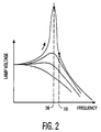
- Fig. 2 is a graph of lamp voltage versus operating frequency.
- Fig. 3 is a schematic diagram of another embodiment of a ballast circuit in accordance with the invention.
- Fig. 1 shows a ballast circuit 10 in accordance with the present invention.
- a gas discharge lamp 12 such as a fluorescent lamp, is powered from a d.c. bus voltage provided by a source 14 and existing between a bus conductor 16 and a reference conductor 18, after such voltage is converted to a.c. Switches 20 and 22, serially connected between conductors 16 and 18, are used in this conversion process.
- the switches comprise n-channel and p-channel enhancement mode MOSFETs, respectively, the source electrodes of the switches are preferably connected directly together at a common node or conductor 24.
- the switches may comprise other devices having complementary conduction modes, such as PNP and NPN Bipolar Junction Transistors.
- An exemplary resonant load circuit 26 includes lamp 12. -A resonant capacitor 28 and a resonant inductor 30 determine frequency of resonance of the load circuit. Circuit 26 also includes a feedback capacitor 32 and a d.c. blocking capacitor 34. A conventional snubber capacitor 36 causes switches 20 and 22 to switch softly.
- Switches 20 and 22 cooperate to provide a.c. current from common node 24 to load circuit 26.
- the gate, or control, electrodes 20a and 22a of the switches preferably are directly connected together at a control node or conductor 32.
- Gate drive circuitry, generally designated 38, is connected between nodes 24 and 32, for regeneratively controlling the switches.
- a feedback signal from the right-hand shown lead of feedback capacitor 32 is coupled to control node 32, preferably via an inductor 40. In addition to providing the feedback signal, capacitor 32 is also used during circuit start-up, as described below.
- a capacitor 44 is preferably provided between nodes 24 and 32 to predictably limit the rate of change of control voltage between such nodes. This beneficially assures, for instance, a dead time interval during switching of switches 20 and 22 wherein both switches are off between the times of either switch being turned on.
- resistors 46 and 48 cooperate with a resistor 50 for starting regenerative operation of gate drive circuit 38.
- capacitor 32 becomes charged upon energizing of source 14, via resistors 46, 48 and 50.
- the voltage across capacitor 32 is zero, and, during the starting process, inductor 40 provides a low impedance charging path.
- resistors 46-50 being of equal value, for instance, the voltage on node 24, upon initial bus energizing, is approximately 1 / 3 of bus voltage 14, and the voltage at node 32, between resistors 46 and 48 is 1 / 3 bus voltage 14.
- capacitor 32 becomes increasingly charged, from right to left as shown, until it reaches the threshold voltage of the gate-to-source voltage of upper switch 20 (e.g., 2-3 volts). At this point, the upper switch starts conducting, which then results in current being supplied by that switch to load circuit 26. In turn, the resulting current in the load circuit causes regenerative control of switches 20 and 22.
- the threshold voltage of the gate-to-source voltage of upper switch 20 e.g., 2-3 volts.
- ballast circuit 10 typically, during steady state operation of ballast circuit 10, d.c. current is blocked from flowing through capacitor 32 by d.c. blocking capacitor 34. This prevents capacitor 32 from building up a d.c. component of offset voltage that could prematurely turn on one of the switches.
- resistor 50 an alternative resistor (not shown) may be placed in shunt across switch 20 rather than across switch 22.
- the operation of the resulting circuit is similar to that described above. However, initially, common node 24 assumes a higher potential than node 32, so that capacitor 32 becomes charged from left to right as shown. The results in an increasingly negative voltage between node 32 and node 24, which turns on switch 22 first.
- Resistors 46 and 48 are both preferably used in the circuit of Fig. 1; however, the circuit functions substantially as intended with resistor 48 removed and using resistor 50. Starting might be somewhat slower and at a higher line voltage. The circuit also functions substantially as intended with resistor 46 removed and using the mentioned alternative resistor (not shown) shunting switch 20.
- a bidirectional voltage clamp 52 is coupled across inductor 40 in such a way as to limit the positive and negative voltage excursions across the inductor. Preferably, it shunts the inductor. Its voltage rating should be sufficiently above that of the control voltage for the switches between nodes 32 and 24 so it does not conduct during normal ballast operation. Setting its voltage rating to double the control voltage has been found sufficient in various embodiments.
- Voltage clamp 52 limits the voltage across the lamp during starting and during lamp operation. If the lamp fails from, for instance, its glass envelope breaking, clamp 52 limits the lamp voltage so that resonant capacitor 28, typically of ceramic, does not overheat and blacken the ballast housing or cause the housing to heat to a smoking condition. Beneficially, the input part of the ballast is more likely to break down more quickly, as for example, by switches 20 and 22 becoming overheated and short-circuited. As such, the ballast can no longer supply power to the lamp, so the lamp and ballast combination can fail without deleterious overheating in the resonant capacitor, for instance.
- Design tolerances of the ballast can be relaxed, reducing component cost. For instance, because there is less stress on the resonant capacitor, a capacitor with a lower rating can be used. Because the peak current of the ballast is lowered, the current rating of the switches can be lowered. Similarly, the resonant inductor can be designed for a lower peak current.
- clamp 42 can be embodied in other ways as will be apparent to those of ordinary skill in the art.
- Fig. 2 shows lamp how lamp voltage varies as a function of frequency of operation. Without clamp 52, output voltage may be at frequency point 56. With clamp 52, the frequency of operation is increased because, by shunting inductor 40, clamp 42 allows capacitor 44 to charge and discharge more quickly. This causes the output voltage to be limited to that at frequency point 58.
- Exemplary component values for the circuit of Fig. 1 are as follows for a fluorescent lamp 12 rated at 11 watts, with a resistance of about 250 ohms, and with a d.c. bus voltage of 300 volts: Resonant inductor 30 2.7 millihenries Resonant capacitor 28 2.2 nanofarads Capacitor 32 33 nanofarads D.c. blocking capacitor 34 100 nanofarads Inductor 40 820 microhenries Capacitor 44 3.3 nanofarads Capacitor 36 470 picofarads Zener diodes 42, each 10 volts Zener diodes 52, each 24 volts Resistors 46, 48 and 50, each 560 k ohms
- switch 20 may be an IRFR310, n-channel, enhancement mode MOSFET, sold by International Rectifier Company, of El Segundo, California; and switch 22, an IRFR9310, p-channel, enhancement mode MOSFET also sold by International Rectifier Company.
- Fig. 3 shows a ballast circuit 10a similar to Fig. 1, but employing different gate drive circuitry 38a.
- Like-numbered parts as between Figs. 1 and 3 refer to similar parts, and description of such parts in Fig. 3 will largely be omitted.
- a feedback inductor 62 is mutually coupled to resonant inductor 30 with polarity as shown by the associated dots for sensing current in load circuit 26a.
- the feedback signal in inductor 62 is coupled to node 32 by inductor 40 and capacitor 64.
- Serially connected resistors 46 and 48 cooperate with a resistor 50 for starting regenerative operation of gate drive circuit 38a.
- capacitor 64 becomes charged upon energizing of source 14, via resistors 46, 48 and 50. Initially, the voltage across capacitor 64 is zero, and, during the starting process, inductors 40 and 62 provide a low impedance charging path.
- resistors 46-50 being of equal value, for instance, the voltage on node 24, upon initial bus energizing, is approximately 1 / 3 of bus voltage 14, and the voltage at node 32 is 1 / 3 bus voltage 14.
- capacitor 64 becomes increasingly charged, from left to right as shown, until it reaches the threshold voltage of the gate-to-source voltage of upper switch 20 (e.g., 2-3 volts).
- the upper switch starts conducting, which then results in current being supplied by that switch to load circuit 26a.
- the resulting current in the load circuit causes regenerative control of switches 20 and 22.
- Exemplary component values for the circuit of Fig. 3 are as follows for a fluorescent lamp 12 rated at 28 watts, with a resistance of about 580 ohms, and with a d.c. bus voltage of 150 volts: Resonant inductor 30 600 microhenries Feedback inductor 62 1.85 microhenries Turns ratio between inductors 30 and 62 18 Resonant capacitor 28 4.7 nanofarads D.c.
- Capacitor 34 220 nanofarads Capacitor 36 470 picofarads Inductor 40 470 microhenries Capacitor 44 1.5 nanofarads Zener diodes 42, each 10 volts Zener diodes 52, each 24 volts Resistors 46, 48 and 50, each 270 k ohms Capacitor 64 100 nanofarads
- Switch 20 may be an IRFR214, n-channel, enhancement mode MOSFET, sold by International Rectifier Company, of El Segundo, California; and switch 22, an IRFR9214, p-channel, enhancement mode MOSFET also sold by International Rectifier Company.
Landscapes
- Circuit Arrangements For Discharge Lamps (AREA)
Applications Claiming Priority (2)
| Application Number | Priority Date | Filing Date | Title |
|---|---|---|---|
| US09/192,785 US6078143A (en) | 1998-11-16 | 1998-11-16 | Gas discharge lamp ballast with output voltage clamping circuit |
| US192785 | 1998-11-16 |
Publications (2)
| Publication Number | Publication Date |
|---|---|
| EP1001662A2 true EP1001662A2 (de) | 2000-05-17 |
| EP1001662A3 EP1001662A3 (de) | 2001-12-19 |
Family
ID=22711039
Family Applications (1)
| Application Number | Title | Priority Date | Filing Date |
|---|---|---|---|
| EP99309111A Withdrawn EP1001662A3 (de) | 1998-11-16 | 1999-11-16 | Elektronisches Vorschaltgerät für Entladungslampen mit Ausgangsspannungsbegrenzung |
Country Status (4)
| Country | Link |
|---|---|
| US (1) | US6078143A (de) |
| EP (1) | EP1001662A3 (de) |
| JP (1) | JP2000150183A (de) |
| CN (1) | CN100386002C (de) |
Cited By (2)
| Publication number | Priority date | Publication date | Assignee | Title |
|---|---|---|---|---|
| EP1258977A3 (de) * | 2001-05-18 | 2004-03-24 | General Electric Company | Selbstschwingender Synchronboostwandler |
| EP1326484A3 (de) * | 2002-01-02 | 2005-01-05 | Patent-Treuhand-Gesellschaft für elektrische Glühlampen mbH | Betriebsgerät für Gasentladungslampen |
Families Citing this family (16)
| Publication number | Priority date | Publication date | Assignee | Title |
|---|---|---|---|---|
| US6483257B1 (en) * | 2000-05-26 | 2002-11-19 | General Electric Company | Ignitor pulse variable reduction method and apparatus |
| US6459215B1 (en) * | 2000-08-11 | 2002-10-01 | General Electric Company | Integral lamp |
| US6555974B1 (en) | 2000-11-21 | 2003-04-29 | General Electric Company | Wiring geometry for multiple integral lamps |
| US6421260B1 (en) | 2000-12-20 | 2002-07-16 | General Electric Company | Shutdown circuit for a half-bridge converter |
| US6433493B1 (en) | 2000-12-27 | 2002-08-13 | General Electric Company | Electronic power converter for triac based controller circuits |
| US6443769B1 (en) | 2001-02-15 | 2002-09-03 | General Electric Company | Lamp electronic end cap for integral lamp |
| US6815908B2 (en) * | 2002-12-11 | 2004-11-09 | General Electric | Dimmable self-oscillating electronic ballast for fluorescent lamp |
| US7276002B2 (en) * | 2003-10-23 | 2007-10-02 | General Motors Corporation | Surface texture configuration for CVT pulley |
| DE10351621B4 (de) * | 2003-11-05 | 2013-05-16 | Osram Gmbh | Elektronisches Vorschaltgerät sowie Verfahren mit bei Ausfall der Licht emittierenden Einrichtung weiterzubetreibenden Wandler |
| DE102005028418A1 (de) * | 2005-06-20 | 2006-12-28 | Patent-Treuhand-Gesellschaft für elektrische Glühlampen mbH | Lampenanschlusspotentialsymmetrierung |
| US7436124B2 (en) * | 2006-01-31 | 2008-10-14 | General Electric Company | Voltage fed inverter for fluorescent lamps |
| US8212498B2 (en) * | 2009-02-23 | 2012-07-03 | General Electric Company | Fluorescent dimming ballast |
| US7990070B2 (en) * | 2009-06-05 | 2011-08-02 | Louis Robert Nerone | LED power source and DC-DC converter |
| US8084949B2 (en) * | 2009-07-09 | 2011-12-27 | General Electric Company | Fluorescent ballast with inherent end-of-life protection |
| US9462660B2 (en) | 2013-02-26 | 2016-10-04 | Lutron Electronics Co., Inc. | Controlling an electronic dimming ballast during low temperature or low mercury conditions |
| US9041454B2 (en) * | 2013-03-15 | 2015-05-26 | Atieva, Inc. | Bias circuit for a switched capacitor level shifter |
Family Cites Families (26)
| Publication number | Priority date | Publication date | Assignee | Title |
|---|---|---|---|---|
| US4677345A (en) * | 1980-08-14 | 1987-06-30 | Nilssen Ole K | Inverter circuits |
| US4370600A (en) * | 1980-11-26 | 1983-01-25 | Honeywell Inc. | Two-wire electronic dimming ballast for fluorescent lamps |
| US4463286A (en) * | 1981-02-04 | 1984-07-31 | North American Philips Lighting Corporation | Lightweight electronic ballast for fluorescent lamps |
| HU181323B (en) * | 1981-05-08 | 1983-07-28 | Egyesuelt Izzolampa | High-frequency system of additional resistor for electric discharge lamp |
| DE3311215A1 (de) * | 1983-03-28 | 1984-10-04 | Patent-Treuhand-Gesellschaft für elektrische Glühlampen mbH, 8000 München | Zuendvorrichtung fuer eine niederdruckentladungslampe |
| US4614897A (en) * | 1984-05-11 | 1986-09-30 | Rca Corporation | Switching circuit |
| US4692667A (en) * | 1984-10-16 | 1987-09-08 | Nilssen Ole K | Parallel-resonant bridge-inverter fluorescent lamp ballast |
| DE3441992A1 (de) * | 1984-11-16 | 1986-05-22 | Patent-Treuhand-Gesellschaft für elektrische Glühlampen mbH, 8000 München | Schaltungsanordnung zur zuendung einer niederdruckentladungslampe |
| US4937470A (en) * | 1988-05-23 | 1990-06-26 | Zeiler Kenneth T | Driver circuit for power transistors |
| US4945278A (en) * | 1988-09-20 | 1990-07-31 | Loong-Tun Chang | Fluorescent tube power supply |
| US5262699A (en) * | 1991-08-26 | 1993-11-16 | Gte Products Corporation | Starting and operating circuit for arc discharge lamp |
| DE4129430A1 (de) * | 1991-09-04 | 1993-03-11 | Patent Treuhand Ges Fuer Elektrische Gluehlampen Mbh | Schaltungsanordnung zum betrieb einer lampe |
| CA2076127A1 (en) * | 1991-09-26 | 1993-03-27 | Louis R. Nerone | Electronic ballast arrangement for a compact fluorescent lamp |
| US5223767A (en) * | 1991-11-22 | 1993-06-29 | U.S. Philips Corporation | Low harmonic compact fluorescent lamp ballast |
| US5309062A (en) * | 1992-05-20 | 1994-05-03 | Progressive Technology In Lighting, Inc. | Three-way compact fluorescent lamp system utilizing an electronic ballast having a variable frequency oscillator |
| US5355055A (en) * | 1992-08-21 | 1994-10-11 | Ganaat Technical Developments Ltd. | Lighting assembly and an electronic ballast therefor |
| US5382882A (en) * | 1993-04-20 | 1995-01-17 | General Electric Company | Power supply circuit for a gas discharge lamp |
| US5387847A (en) * | 1994-03-04 | 1995-02-07 | International Rectifier Corporation | Passive power factor ballast circuit for the gas discharge lamps |
| US5406177A (en) * | 1994-04-18 | 1995-04-11 | General Electric Company | Gas discharge lamp ballast circuit with compact starting circuit |
| US5514981A (en) * | 1994-07-12 | 1996-05-07 | International Rectifier Corporation | Reset dominant level-shift circuit for noise immunity |
| US5619106A (en) * | 1996-06-24 | 1997-04-08 | General Electric Company | Diodeless start circiut for gas discharge lamp having a voltage divider connected across the switching element of the inverter |
| US5952790A (en) * | 1996-09-06 | 1999-09-14 | General Electric Company | Lamp ballast circuit with simplified starting circuit |
| CN1177900A (zh) * | 1996-09-06 | 1998-04-01 | 通用电气公司 | 用于气体放电灯的镇流电路 |
| US5917289A (en) * | 1997-02-04 | 1999-06-29 | General Electric Company | Lamp ballast with triggerless starting circuit |
| US5796214A (en) * | 1996-09-06 | 1998-08-18 | General Elecric Company | Ballast circuit for gas discharge lamp |
| US5945783A (en) * | 1998-07-13 | 1999-08-31 | General Electric Company | Zero energy-storage ballast for compact fluorescent lamps |
-
1998
- 1998-11-16 US US09/192,785 patent/US6078143A/en not_active Expired - Lifetime
-
1999
- 1999-11-08 JP JP11316157A patent/JP2000150183A/ja not_active Withdrawn
- 1999-11-16 CN CNB991244591A patent/CN100386002C/zh not_active Expired - Fee Related
- 1999-11-16 EP EP99309111A patent/EP1001662A3/de not_active Withdrawn
Cited By (2)
| Publication number | Priority date | Publication date | Assignee | Title |
|---|---|---|---|---|
| EP1258977A3 (de) * | 2001-05-18 | 2004-03-24 | General Electric Company | Selbstschwingender Synchronboostwandler |
| EP1326484A3 (de) * | 2002-01-02 | 2005-01-05 | Patent-Treuhand-Gesellschaft für elektrische Glühlampen mbH | Betriebsgerät für Gasentladungslampen |
Also Published As
| Publication number | Publication date |
|---|---|
| CN1261762A (zh) | 2000-08-02 |
| JP2000150183A (ja) | 2000-05-30 |
| CN100386002C (zh) | 2008-04-30 |
| US6078143A (en) | 2000-06-20 |
| EP1001662A3 (de) | 2001-12-19 |
Similar Documents
| Publication | Publication Date | Title |
|---|---|---|
| US6078143A (en) | Gas discharge lamp ballast with output voltage clamping circuit | |
| US5796214A (en) | Ballast circuit for gas discharge lamp | |
| EP0679049B1 (de) | Vorschaltgerät für eine Entladungslampe | |
| US5965985A (en) | Dimmable ballast with complementary converter switches | |
| EP1987705B1 (de) | Spannungsgespeister wandler für leuchtstofflampen | |
| EP1286574B1 (de) | Vorschaltgerät mit effizienter Elektroden-Vorheizung und Lampenfehlerschutz | |
| US6867553B2 (en) | Continuous mode voltage fed inverter | |
| EP0659037B1 (de) | Vorschaltgerät für eine Entladungslampe, mit Arbeitsfähigkeitsanzeige | |
| US5917289A (en) | Lamp ballast with triggerless starting circuit | |
| US5952790A (en) | Lamp ballast circuit with simplified starting circuit | |
| CA2153108C (en) | Semiconductor-controlled operating circuit for one or more low-pressur discharge lamps, typically fluorescent lamps | |
| US6815908B2 (en) | Dimmable self-oscillating electronic ballast for fluorescent lamp | |
| US6198231B1 (en) | Circuit configuration for operating at least one discharge lamp | |
| JPH11252933A (ja) | 負荷の作動回路 | |
| KR20100122463A (ko) | 저압 가스 방전 램프를 동작시키기 위한 회로 어레인지먼트 및 대응 방법 | |
| MXPA02006111A (es) | Circuito de proteccion de recebado caliente para un inductor autorregulador de lampara auto-oscilante. | |
| US6657400B2 (en) | Ballast with protection circuit for preventing inverter startup during an output ground-fault condition | |
| CA2306815A1 (en) | Circuit arrangement for operating at least one discharge lamp | |
| US6111363A (en) | Ballast shutdown circuit for a gas discharge lamp | |
| US6756746B2 (en) | Method of delaying and sequencing the starting of inverters that ballast lamps | |
| US6057648A (en) | Gas discharge lamp ballast with piezoelectric transformer | |
| EP0759265B1 (de) | Umschaltanordnung | |
| US6150769A (en) | Gas discharge lamp ballast with tapless feedback circuit | |
| US5986410A (en) | Integrated circuit for use in a ballast circuit for a gas discharge lamp | |
| JP2011520224A (ja) | 電圧給電型プログラム始動式安定器 |
Legal Events
| Date | Code | Title | Description |
|---|---|---|---|
| PUAI | Public reference made under article 153(3) epc to a published international application that has entered the european phase |
Free format text: ORIGINAL CODE: 0009012 |
|
| AK | Designated contracting states |
Kind code of ref document: A2 Designated state(s): AT BE CH CY DE DK ES FI FR GB GR IE IT LI LU MC NL PT SE Kind code of ref document: A2 Designated state(s): DE FR GB IT |
|
| AX | Request for extension of the european patent |
Free format text: AL;LT;LV;MK;RO;SI |
|
| PUAL | Search report despatched |
Free format text: ORIGINAL CODE: 0009013 |
|
| AK | Designated contracting states |
Kind code of ref document: A3 Designated state(s): AT BE CH CY DE DK ES FI FR GB GR IE IT LI LU MC NL PT SE |
|
| AX | Request for extension of the european patent |
Free format text: AL;LT;LV;MK;RO;SI |
|
| RIC1 | Information provided on ipc code assigned before grant |
Free format text: 7H 05B 41/285 A, 7H 05B 41/282 B |
|
| STAA | Information on the status of an ep patent application or granted ep patent |
Free format text: STATUS: THE APPLICATION HAS BEEN WITHDRAWN |
|
| 17P | Request for examination filed |
Effective date: 20020619 |
|
| AKX | Designation fees paid |
Free format text: DE FR GB IT |
|
| 18W | Application withdrawn |
Withdrawal date: 20020812 |