EP1003129A2 - Méthode et appareil pour le changement de dimension d'une image vidéo - Google Patents
Méthode et appareil pour le changement de dimension d'une image vidéo Download PDFInfo
- Publication number
- EP1003129A2 EP1003129A2 EP99308969A EP99308969A EP1003129A2 EP 1003129 A2 EP1003129 A2 EP 1003129A2 EP 99308969 A EP99308969 A EP 99308969A EP 99308969 A EP99308969 A EP 99308969A EP 1003129 A2 EP1003129 A2 EP 1003129A2
- Authority
- EP
- European Patent Office
- Prior art keywords
- source
- pixels
- pixel
- area
- target
- Prior art date
- Legal status (The legal status is an assumption and is not a legal conclusion. Google has not performed a legal analysis and makes no representation as to the accuracy of the status listed.)
- Granted
Links
Images






Classifications
-
- G—PHYSICS
- G06—COMPUTING OR CALCULATING; COUNTING
- G06T—IMAGE DATA PROCESSING OR GENERATION, IN GENERAL
- G06T3/00—Geometric image transformations in the plane of the image
- G06T3/40—Scaling of whole images or parts thereof, e.g. expanding or contracting
Definitions
- This invention relates to image processing and in particular to a method and apparatus for resizing digital video display signals so that the image can be displayed at a different size to the original size of the incoming display signals.
- the resizing of digital video display signals is well known and is employed in a number of environments. For example it may be desired to shrink, or minify, an XGA image of 1024 x 768 pixels for display on a S-VGA display of 800 x 600 pixels. It may be desired to greatly expand, or magnify or zoom, a digital video signal (existing as, for example, a TV signal or a stored video signal such as on a video cassette or disc) for display on a multiscreen videowall.
- a digital video signal existing as, for example, a TV signal or a stored video signal such as on a video cassette or disc
- the present invention provides a new approach to image resizing using a single sampling technique so that source pixels are converted directly into target pixels without intermediate upsampling.
- the approach enables fast resizing to occur in real time and both minification and magnification may be conducted with the same firmware.
- Better image resolution is achieved by maintaining the frequency content of the original image to be proportional to the resized picture in order to minimise aliasing whilst preserving image fidelity.
- the present invention is based on expressing the amount of energy (brightness) associated with each sampled source pixel to span an area of two samples in duration.
- the area span has a triangular area that is designed to be proportional to the linear energy distribution of the source pixel.
- This linear energy representation in a discrete sampled domain avoids the need for the classical intermediate up sampled step in deriving target pixels for any resized factor. From an algorithm based on this principle a set of coefficients are determined that map source to target pixels as a function of resize factor.
- the present invention provides a method and apparatus for image processing as specified in the claims hereinafter.
- Figure 1 depicts how the energy distribution of successive source pixels can be depicted by a series of triangular areas.
- Figure 2 shows how the target pixel brightness can be calculated from a series of triangular areas.
- Figure 3 shows how a single source pixel triangular area can be sub sampled to produce sub areas.
- Figures 4A, B, and C show three different conditions in which source pixel intervals are related to target pixel intervals
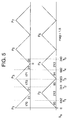
- Figure 5 is an example showing a magnification of 1.5
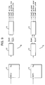
- Figure 6 is an example showing a magnification of 0.75 (i.e. a minification);
- Figure 7 is a block diagram showing the complete inputs and outputs to an apparatus forming a preferred embodiment of the invention which is given by way of example;
- Figure 8 is a more detailed block diagram showing how the apparatus is broken up into two blocks: a control print section and scaler(s);
- Figure 9 is a schematic circuit diagram detailing the control print section of Figure 8.
- Figure 10 is a circuit diagram of the sample number, Sn, generator block of Figure 9;
- Figure 11 is a circuit diagram of the Sn-sqd block of Figure 9;
- Figure 12 is a circuit diagram of the coefficient switch block of Figure 9;
- Figure 13 is a circuit diagram of the scaler block of Figure 8.
- Figure 14 is a circuit diagram of the line delay block shown in Figure 13;
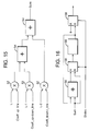
- Figure 15 is a circuit diagram of the line summer block shown in Figure 13;
- Figure 16 is a circuit diagram of the line accumulator block shown in Figure 13.
- each source pixel of an incoming picture signal is sampled and represented by a triangular area that spans two sample periods and defines its linear energy distribution.
- the energy, represented by the area of the triangle can be thought of as being represented by an infinite set of linear samples extending vertically, commencing, for the source pixel Pn, at point A (where the energy is zero), increasing in brightness to a maximum at the apex, Pn, and decreasing to zero at point B.
- the output pixel samples can be calculated by considering the area contribution of source pixels described between the boundaries of target samples. Note these boundaries will be asynchronous and will produce summations of partial source areas. It will be appreciated that the process of magnification will produce more output pixel samples than source samples, and minification the opposite.
- the brightness of the target pixel for the sampling interval illustrated can be considered to be represented by the proportion of area 1 to the total area of Pn-1 plus the proportion of area 2 to the total area of P(n), plus the proportion of area 3 to the total area of Pn+1.
- P(n-1), P(n), P(n+1) are the brightness values of the source pixels and T(n) is target pixel brightness value
- P(n) is target pixel brightness value
- the complexity of pixel area calculations may be simplified by deriving a series of general equations that work on the principle of differences.
- Figure 3 shows a typical series of samples of a pixel (in this case 5 samples, numbered 1 to 5).
- Area 1 Sn 2 2
- Area 2 (Sn+1) 2 2 - Sn 2 2
- Area 3 1- (Sn+1) 2 2 - (1-Sn+2) 2
- Area 4 (1-Sn+2) 2 2 - (1-Sn+3) 2
- Area 5 (1-Sn+4) 2 2
- any magnification/minification will produce samples whose areas can be defined by one or more of the above 5 areas.
- the source pixel interval and the sample pixel interval generally move asynchronously.
- the value Sn is the time of arrival of the next target pixel boundary after the point of maximum brightness for the previous source pixel.
- point X is at time Sn-1 after the arrival of Pn-1
- point Y is at time Sn after the arrival of Pn etc.
- the generalised value Sn will vary from target pixel to target pixel and needs to be calculated each time in the algorithm giving target pixel brightness.
- the brightness area computation is made up of a "down” sample, an "up down” sample, and an "up” sample.
- the "down sample” is area E
- the "up down” sample is area F
- the "up” sample is area G.
- the algorithm determines the value of Sn and whether or not a "not next", “next”, or “shrink” condition exists from the size signal (11) defined above.
- the computation for our preferred embodiment is as follows. Accumulate the size signal, by its own value, each time a target pixel falls to be computed. If the value exceeds 4095, but not 8191, then this demonstrates a "next” condition. If the value exceeds 4095, the end number 4095 rolls over, leaving the remainder. For the succeeding target pixel, reaccumulate the size value from the remainder. Keep repeating this. If an any time the accumulated value exceeds 8191, then this demonstrates a "shrink" condition. If the value exceeds 8191, the end number 8191 rolls over leaving the remainder. Then re-accumulate size from the remainder.
- the accumulated size value can be expressed thus:
- the value of the accumulated size value can be expressed in the following truth table.
- Bit No. Decimal Shrink Next 15 14 13 12 11........2,1,0 size value 0 0 0 0 0 0..........00 0 0 0 0 0 0 0..........01 1 0 1 0 0 0 1 0..........00 4096 1 1 0 0 1 0 0..........01 8193 : : : : : :............: : : 1 1 1 1 1 1..........11 65535
- the value of the number held in bits 12 to 15 determines the number of times the algorithm must be repeated (and the results accumulated) in a shrink condition.
- Sn The value of Sn is obtained from the value held by bits 0 to 11 after any reset has taken place.
- the twelve bit number is decimated to 10 bits, by mapping bit 11 to bit 9, bit 10 to bit 8, ising bit 2 to bit 0 and discarding bits 0 and 1. This effectively divides by 4. Although this results in a loss of resolution, it increases processing speed, and is visually not noticeable to the naked eye.
- RGB pixels are resized separately using the above described algorithm.
- the summed coefficients amount to approximately 256 (the approximation arises from the rounding errors).
- the summed coefficients always come to this constant value as this represents the unitised brightness value. In other words, the areas that represent pixel energy that make up the target pixel maintain the original picture brightness.
- Equations 4 and 5 For each target pixel, firstly use Sn and Sn+1 to calculate Equations 4 and 5 and apply these results to Equations 6 to 10 according to whether the target condition is "not next”, “next", or "shrink". T1 is a not next condition and the P(1) coeffs are calculated from equations 7 and 9
- a convolver which accepts source pixels in a raster scan of successive lines, and from which computes target pixels in target lines in accordance with the invention will now be described, by way of example, with reference to Figures 7 to 16.
- clock and reset signals have been omitted for clarity. The skilled person will appreciate how to implement such signals without difficulty.
- the complete convolver showing the various essential inputs and outputs is shown in Figure 7.
- the brightness value for each individual source pixel arrives as an 8-bit signal P(n).
- P(n) 8-bit signal
- SZ(L) size signal equation (11)
- SZ(P) size signal equation (11)
- SC(L) and SC(P) separate inputs for the size signal equation (11) above, SZ(L) for line sizing and SZ(P) for pixel sizing exist, as well as separate corresponding scale values, SC(L) and SC(P).
- the output is a target pixel brightness signal of 8 bits width, T(n).
- the convolver can be broken down into two sections, as shown in Figure 8.
- the two sections consist of a control print section 2 and (in the case of a convolver handling R, G and B colour pixels) three scalers in parallel, only one of which, 4, has been shown for clarity.
- One scaler operates on R pixels, a second on G pixels, and a third on B pixels. They operate identically in parallel, hence only one needs to be described.
- the control print section 2 is shown in more detail in Figure 9. It consists of a line channel 6, to provide the parameters for scaling complete lines of pixels (i.e. in the y-direction) and a pixel channel 8 to provide the parameters for scaling each individual pixel (i.e. in the x-direction).
- Each channel includes a sample number, Sn, generator circuit 10. This generates the sample interval for the target lines and pixels. This is followed by an Sn-sqd circuit 12 which generates the equation 4 and 5 values which are themselves used to generate equations (6) to (10) above.
- Circuit 12 leads to a coefficient switch circuit 14 which generates, in each channel, three signals: Coeff-up Coeff-up-down Coeff-down-1.
- the Sn generator circuit 10 is shown schematically in Figure 10. It consists of a size increment block 16, a shrink hold block 18, and an Sn output block 20. The manner in which these blocks operate will be described below.
- the Sn-sqd circuit 12 is shown in more detail in Figure 11. It consists of a multiplier 22 which squares the Sn input signal to provide (Sn) 2 for the equation 4 signal, a subtractor 24 which generates, in our example, (1024-Sn), with 1024 being input as a constant, C, to the subtractor, and a further multiplier 26 to provide (1024-Sn) 2 for the equation 5 signal.
- a divide-by-1024 is also provided by multipliers 22, 26.
- the coefficient switch circuit 14 is detailed in Figure 12. It consists of sample delays 28, an adder 30, subtractors 32, switches 34 and multipliers 36. As mentioned above circuit 14 provides 3 outputs and these are provided according to the following truth table: Next Coeff-up Coeff-up-down Coeff-down-1 Not active Sn-up-diff Sn-down-diff - Active Sn-up Sn-up-down Sn-down
- the coefficient switch circuit uses the generalised equations (6) to (10) above, the coefficient switch circuit generates selected ones of the equations dependant on whether or not Next is active (i.e. whether or not a next condition exists).
- Next Coeff-up Coeff-up-down Coeff-down-1 not active eqn(7) eqn(9) - Active eqn(6) eqn(8) eqn(10)
- next bit (12th bit) in the 16 bit accumulated size value is active (binary 1)
- various of the equations (6) to (10) are routed to the three outputs of switch 14.
- the next signal acts as the selector for switches 34 causing the appropriate signal to be outputted.
- the switches 34 select channels B causing the values for equations (6) , (8) and (10) to be forwarded to the multipliers, for multiplication by the SC scale value.
- the multipliers also provide a divide-by-2 function (which appears in the denominators of equations (6) to (10)).
- Next is not active, the values for equations (7) and (9) are routed. Next is also forced to be active when a shrink condition exists.
- Each (of the three) scalers consists of a line scaler 38 in series with a pixel scaler 40.
- the line and pixel scalers work independently of one another.
- the line scaler scales in the y-direction and acts upon complete lines of pixels in blocks, with the same scaling factor being applied to each individual pixel in the same line.
- the line-scaled pixels are then operated on by the pixel scaler.
- the latter scales in the x-direction and scales successive individual pixels one by one.
- Each of the line and pixel scalers consist of a delay 42, a summer 44, and an accumulator 46.
- the line delay is shown in Figure 14. It consists of switches 48 and line delays 50.
- the line delay provides outputs consisting of the brightness data for all the pixels in three successive lines, shown as L, L-1, L-2. This provides the requirement for the algorithm used in the invention which processes line data from three successive lines simultaneously.
- Each line delay consists of a series of stored pixels of one line length.
- the pixel delay (shown in Figure 13) is identical to the line delay except that it delays individual successive pixels rather than complete lines of pixels. It provides the output for three successive pixels Pn, Pn-1, Pn-2. This again meets the requirement of the algorithm. Each pixel delay is for one pixel.
- the line summer is shown in Figure 15. It consists of three multipliers 52 and two adders 54.
- the summer firstly multiplies the pixel brightness values for each pixel in a line by the coefficient value provided by the coefficient switch circuit 14, i.e. by the result of the computation of the appropriate one of the equations (6) to (10). Each pixel in any one line is multiplied by the same coefficient. The results of these three multiplications are then summed to provide the appropriate brightness information for each line of target pixels.
- the pixel summer (shown in Figure 13) is identical to the line summer except that it multiplies the brightness values of individual pixels against coefficient values which will normally differ from successive pixel to pixel. Each pixel is operated on independently.
- the line accumulator is shown in detail in Figure 16. It consists of an adder 56, switches 58, and a line delay 60. It receives the summed output of the summer ( Figure 15) and is controlled by the shrink signal.
- the accumulator is only active when a shrink condition exists, i.e. only when any one or more of the top three bits of the 16-bit accumulated size signal are active (not 0).
- the accumulator is non-functional and the sum input is passed straight through and out as an 8-bit target line consisting of a series of 8 bit pixels.
- the summer 56 accumulates the sum values from successive sets of three lines for as many passes as is required to satisfy the shrink condition prevailing.
- the shrink signal forces the output of the second switch to zero : no target line data is available at the output until sufficient passes have taken place to satisfy the shrink.
- the accumulated sum in adder 56 is then released as the output.
- the pixel accumulator is identical to the line accumulator except that it operates on the sums resulting from 3 successive pixels rather than sums resulting from 3 successive lines of pixels.
- the output of the pixel accumulator is a series of pixels which have thus been scaled line-by-line wise in the y-direction and pixel-by-pixel wise in the x-direction.
- the output of the pixel accumulator is thus the final rescaled target pixels.
- the convolver operates to implement the algorithm as follows.
- the Sn generator circuit 10 receives the size (Sz) value (which is a constant for each magnification).
- the shrink hold block 16 receives the 4-bit output and provides a shrink-cntrl output which returns to control the size increment block 16.
- shrink-cntrl When shrink-cntrl is active, the size increment block is held active for the appropriate number of shrink cycles (passes).
- the following truth table details the correspondence of Sz-inc(15-12), Next, and shrink-hold.
- the Sn output block 20 provides control outputs as a function of Sz-Inc(11-0), shrink-insert and Next.
- the Sn-sqd circuit 12 receives the 10-bit Sn value and generates, for successive pixels or lines, the equation 4 and 5 values. From these, the coefficient switch circuit 14 generates the values from the various equations (6) to (10) dependent on whether or not Next is active.
- the scaler 4 receives the pixel brightness information, pixel-by-pixel, and the three coeff values.
- line scaler 38 as has been described, complete lines of pixels are multiplied by the same coefficient value and this is generated for each of three successive lines in summer 44. If shrink is active, these sums are accumulated for the appropriate number of cycles (passes) in line accumulator 46 - see the last truth table above.
Landscapes
- Physics & Mathematics (AREA)
- General Physics & Mathematics (AREA)
- Engineering & Computer Science (AREA)
- Theoretical Computer Science (AREA)
- Image Processing (AREA)
- Editing Of Facsimile Originals (AREA)
- Studio Circuits (AREA)
- Controls And Circuits For Display Device (AREA)
- Closed-Circuit Television Systems (AREA)
- Ultra Sonic Daignosis Equipment (AREA)
- Holo Graphy (AREA)
Applications Claiming Priority (2)
| Application Number | Priority Date | Filing Date | Title |
|---|---|---|---|
| GBGB9825379.2A GB9825379D0 (en) | 1998-11-19 | 1998-11-19 | Image processing |
| GB9825379 | 1998-11-19 |
Publications (3)
| Publication Number | Publication Date |
|---|---|
| EP1003129A2 true EP1003129A2 (fr) | 2000-05-24 |
| EP1003129A3 EP1003129A3 (fr) | 2000-12-13 |
| EP1003129B1 EP1003129B1 (fr) | 2006-04-12 |
Family
ID=10842720
Family Applications (1)
| Application Number | Title | Priority Date | Filing Date |
|---|---|---|---|
| EP99308969A Expired - Lifetime EP1003129B1 (fr) | 1998-11-19 | 1999-11-11 | Méthode et appareil pour le changement de dimension d'une image vidéo |
Country Status (6)
| Country | Link |
|---|---|
| US (1) | US6594404B1 (fr) |
| EP (1) | EP1003129B1 (fr) |
| JP (1) | JP4643781B2 (fr) |
| AT (1) | ATE323310T1 (fr) |
| DE (1) | DE69930815T2 (fr) |
| GB (1) | GB9825379D0 (fr) |
Families Citing this family (4)
| Publication number | Priority date | Publication date | Assignee | Title |
|---|---|---|---|---|
| US20050201640A1 (en) * | 2004-03-10 | 2005-09-15 | Wen-Kuo Lin | Digital picture scaling |
| US7551806B2 (en) * | 2005-07-28 | 2009-06-23 | Etron Technology, Inc. | Two stage interpolation apparatus and method for up-scaling an image on display device |
| US8035682B2 (en) * | 2006-12-21 | 2011-10-11 | Universal City Studios Llc | Moving screen image assembler |
| WO2015115168A1 (fr) * | 2014-01-28 | 2015-08-06 | シャープ株式会社 | Dispositif de traitement d'image |
Family Cites Families (12)
| Publication number | Priority date | Publication date | Assignee | Title |
|---|---|---|---|---|
| US5202670A (en) * | 1986-08-20 | 1993-04-13 | Canon Kabushiki Kaisha | Image processing apparatus |
| JP2724224B2 (ja) * | 1989-11-15 | 1998-03-09 | 株式会社東芝 | ディジタル画像信号の変倍処理方法および装置 |
| US5282051A (en) * | 1991-07-29 | 1994-01-25 | Xerox Corporation | Apparatus and method for performing resolution conversion on image data with auto correlation |
| JP2860039B2 (ja) * | 1993-05-20 | 1999-02-24 | シャープ株式会社 | 擬似中間調画像縮小装置 |
| US5790714A (en) * | 1994-11-01 | 1998-08-04 | International Business Machines Corporation | System and method for scaling video |
| JP3823333B2 (ja) * | 1995-02-21 | 2006-09-20 | 株式会社日立製作所 | 動画像の変化点検出方法、動画像の変化点検出装置、動画像の変化点検出システム |
| US5696848A (en) * | 1995-03-09 | 1997-12-09 | Eastman Kodak Company | System for creating a high resolution image from a sequence of lower resolution motion images |
| US5796879A (en) * | 1995-05-23 | 1998-08-18 | Hewlett-Packard Company | Area based interpolation for image scaling |
| JP3596194B2 (ja) * | 1996-10-29 | 2004-12-02 | ソニー株式会社 | 画像処理装置および方法 |
| JP3742167B2 (ja) * | 1996-12-18 | 2006-02-01 | 株式会社東芝 | 画像表示制御装置 |
| US6348929B1 (en) * | 1998-01-16 | 2002-02-19 | Intel Corporation | Scaling algorithm and architecture for integer scaling in video |
| JP2000207391A (ja) * | 1998-11-10 | 2000-07-28 | Sony Corp | 補間装置、補間方法及び画像表示装置 |
-
1998
- 1998-11-19 GB GBGB9825379.2A patent/GB9825379D0/en not_active Ceased
-
1999
- 1999-11-04 US US09/433,425 patent/US6594404B1/en not_active Expired - Lifetime
- 1999-11-11 AT AT99308969T patent/ATE323310T1/de not_active IP Right Cessation
- 1999-11-11 EP EP99308969A patent/EP1003129B1/fr not_active Expired - Lifetime
- 1999-11-11 DE DE69930815T patent/DE69930815T2/de not_active Expired - Lifetime
- 1999-11-19 JP JP32966699A patent/JP4643781B2/ja not_active Expired - Fee Related
Also Published As
| Publication number | Publication date |
|---|---|
| DE69930815D1 (de) | 2006-05-24 |
| JP2000163041A (ja) | 2000-06-16 |
| GB9825379D0 (en) | 1999-01-13 |
| EP1003129B1 (fr) | 2006-04-12 |
| JP4643781B2 (ja) | 2011-03-02 |
| ATE323310T1 (de) | 2006-04-15 |
| EP1003129A3 (fr) | 2000-12-13 |
| DE69930815T2 (de) | 2006-10-19 |
| US6594404B1 (en) | 2003-07-15 |
Similar Documents
| Publication | Publication Date | Title |
|---|---|---|
| US6389180B1 (en) | Resolution conversion system and method | |
| JP2612939B2 (ja) | イメージ表示システム用補間装置およびイメージ表示システム | |
| US4213150A (en) | Real-time edge processing unit | |
| EP0513516A2 (fr) | Procédé et appareil pour la réduction d'images numériques | |
| US7391904B2 (en) | Correlation-based color mosaic interpolation adjustment using luminance gradients | |
| US4653013A (en) | Altering spatial characteristics of a digital image | |
| US5555359A (en) | Computer graphics anti-aliasing method using a partitioned look-up table | |
| KR960009610A (ko) | 영상 스케일링 필터 및 비디오 스케일링을 제공하는 방법 | |
| JP5080678B2 (ja) | 二次元画像の透視変換 | |
| JPH08331377A (ja) | 画像を変倍する方法 | |
| JP2837339B2 (ja) | 画像生成方法 | |
| US5930407A (en) | System and method for efficiently generating cubic coefficients in a computer graphics system | |
| EP0182243B1 (fr) | Filtrage de signal d'image | |
| US6539128B1 (en) | Method and apparatus for interpolation | |
| US6594404B1 (en) | Image processing | |
| US6643412B1 (en) | Method and apparatus for high speed convolution | |
| JPH04190466A (ja) | カラー画像の限定色表現装置 | |
| US5926580A (en) | Convolution algorithm for efficient hardware implementation | |
| JP2658089B2 (ja) | カラー画像処理方法 | |
| JPH0814843B2 (ja) | 色変換方法および色変換装置 | |
| JP3059287B2 (ja) | 2値画像変倍装置 | |
| EP0684577B1 (fr) | Méthode d'extraction de caractéristiques d'images numériques binaires | |
| JP2916607B2 (ja) | 画像拡大装置 | |
| JP2658086B2 (ja) | カラー画像処理方法 | |
| JP3006522B2 (ja) | 減色処理装置 |
Legal Events
| Date | Code | Title | Description |
|---|---|---|---|
| PUAI | Public reference made under article 153(3) epc to a published international application that has entered the european phase |
Free format text: ORIGINAL CODE: 0009012 |
|
| AK | Designated contracting states |
Kind code of ref document: A2 Designated state(s): AT BE CH CY DE DK ES FI FR GB GR IE IT LI LU MC NL PT SE |
|
| AX | Request for extension of the european patent |
Free format text: AL;LT;LV;MK;RO;SI |
|
| PUAL | Search report despatched |
Free format text: ORIGINAL CODE: 0009013 |
|
| AK | Designated contracting states |
Kind code of ref document: A3 Designated state(s): AT BE CH CY DE DK ES FI FR GB GR IE IT LI LU MC NL PT SE |
|
| AX | Request for extension of the european patent |
Free format text: AL;LT;LV;MK;RO;SI |
|
| 17P | Request for examination filed |
Effective date: 20010521 |
|
| AKX | Designation fees paid |
Free format text: AT BE CH CY DE DK ES FI FR GB GR IE IT LI LU MC NL PT SE |
|
| 17Q | First examination report despatched |
Effective date: 20030523 |
|
| GRAP | Despatch of communication of intention to grant a patent |
Free format text: ORIGINAL CODE: EPIDOSNIGR1 |
|
| GRAS | Grant fee paid |
Free format text: ORIGINAL CODE: EPIDOSNIGR3 |
|
| GRAA | (expected) grant |
Free format text: ORIGINAL CODE: 0009210 |
|
| AK | Designated contracting states |
Kind code of ref document: B1 Designated state(s): AT BE CH CY DE DK ES FI FR GB GR IE IT LI LU MC NL PT SE |
|
| PG25 | Lapsed in a contracting state [announced via postgrant information from national office to epo] |
Ref country code: NL Free format text: LAPSE BECAUSE OF FAILURE TO SUBMIT A TRANSLATION OF THE DESCRIPTION OR TO PAY THE FEE WITHIN THE PRESCRIBED TIME-LIMIT Effective date: 20060412 Ref country code: LI Free format text: LAPSE BECAUSE OF FAILURE TO SUBMIT A TRANSLATION OF THE DESCRIPTION OR TO PAY THE FEE WITHIN THE PRESCRIBED TIME-LIMIT Effective date: 20060412 Ref country code: IT Free format text: LAPSE BECAUSE OF FAILURE TO SUBMIT A TRANSLATION OF THE DESCRIPTION OR TO PAY THE FEE WITHIN THE PRESCRIBED TIME-LIMIT;WARNING: LAPSES OF ITALIAN PATENTS WITH EFFECTIVE DATE BEFORE 2007 MAY HAVE OCCURRED AT ANY TIME BEFORE 2007. THE CORRECT EFFECTIVE DATE MAY BE DIFFERENT FROM THE ONE RECORDED. Effective date: 20060412 Ref country code: FI Free format text: LAPSE BECAUSE OF FAILURE TO SUBMIT A TRANSLATION OF THE DESCRIPTION OR TO PAY THE FEE WITHIN THE PRESCRIBED TIME-LIMIT Effective date: 20060412 Ref country code: CH Free format text: LAPSE BECAUSE OF FAILURE TO SUBMIT A TRANSLATION OF THE DESCRIPTION OR TO PAY THE FEE WITHIN THE PRESCRIBED TIME-LIMIT Effective date: 20060412 Ref country code: BE Free format text: LAPSE BECAUSE OF FAILURE TO SUBMIT A TRANSLATION OF THE DESCRIPTION OR TO PAY THE FEE WITHIN THE PRESCRIBED TIME-LIMIT Effective date: 20060412 Ref country code: AT Free format text: LAPSE BECAUSE OF FAILURE TO SUBMIT A TRANSLATION OF THE DESCRIPTION OR TO PAY THE FEE WITHIN THE PRESCRIBED TIME-LIMIT Effective date: 20060412 |
|
| REG | Reference to a national code |
Ref country code: GB Ref legal event code: FG4D |
|
| REG | Reference to a national code |
Ref country code: CH Ref legal event code: EP |
|
| REF | Corresponds to: |
Ref document number: 69930815 Country of ref document: DE Date of ref document: 20060524 Kind code of ref document: P |
|
| REG | Reference to a national code |
Ref country code: IE Ref legal event code: FG4D |
|
| PG25 | Lapsed in a contracting state [announced via postgrant information from national office to epo] |
Ref country code: SE Free format text: LAPSE BECAUSE OF FAILURE TO SUBMIT A TRANSLATION OF THE DESCRIPTION OR TO PAY THE FEE WITHIN THE PRESCRIBED TIME-LIMIT Effective date: 20060712 Ref country code: DK Free format text: LAPSE BECAUSE OF FAILURE TO SUBMIT A TRANSLATION OF THE DESCRIPTION OR TO PAY THE FEE WITHIN THE PRESCRIBED TIME-LIMIT Effective date: 20060712 |
|
| PG25 | Lapsed in a contracting state [announced via postgrant information from national office to epo] |
Ref country code: ES Free format text: LAPSE BECAUSE OF FAILURE TO SUBMIT A TRANSLATION OF THE DESCRIPTION OR TO PAY THE FEE WITHIN THE PRESCRIBED TIME-LIMIT Effective date: 20060723 |
|
| PG25 | Lapsed in a contracting state [announced via postgrant information from national office to epo] |
Ref country code: PT Free format text: LAPSE BECAUSE OF FAILURE TO SUBMIT A TRANSLATION OF THE DESCRIPTION OR TO PAY THE FEE WITHIN THE PRESCRIBED TIME-LIMIT Effective date: 20060912 |
|
| NLV1 | Nl: lapsed or annulled due to failure to fulfill the requirements of art. 29p and 29m of the patents act | ||
| REG | Reference to a national code |
Ref country code: CH Ref legal event code: PL |
|
| PG25 | Lapsed in a contracting state [announced via postgrant information from national office to epo] |
Ref country code: IE Free format text: LAPSE BECAUSE OF NON-PAYMENT OF DUE FEES Effective date: 20061113 |
|
| ET | Fr: translation filed | ||
| PG25 | Lapsed in a contracting state [announced via postgrant information from national office to epo] |
Ref country code: MC Free format text: LAPSE BECAUSE OF NON-PAYMENT OF DUE FEES Effective date: 20061130 |
|
| PLBE | No opposition filed within time limit |
Free format text: ORIGINAL CODE: 0009261 |
|
| STAA | Information on the status of an ep patent application or granted ep patent |
Free format text: STATUS: NO OPPOSITION FILED WITHIN TIME LIMIT |
|
| 26N | No opposition filed |
Effective date: 20070115 |
|
| PG25 | Lapsed in a contracting state [announced via postgrant information from national office to epo] |
Ref country code: GR Free format text: LAPSE BECAUSE OF FAILURE TO SUBMIT A TRANSLATION OF THE DESCRIPTION OR TO PAY THE FEE WITHIN THE PRESCRIBED TIME-LIMIT Effective date: 20060713 |
|
| PG25 | Lapsed in a contracting state [announced via postgrant information from national office to epo] |
Ref country code: LU Free format text: LAPSE BECAUSE OF NON-PAYMENT OF DUE FEES Effective date: 20061111 |
|
| PG25 | Lapsed in a contracting state [announced via postgrant information from national office to epo] |
Ref country code: CY Free format text: LAPSE BECAUSE OF FAILURE TO SUBMIT A TRANSLATION OF THE DESCRIPTION OR TO PAY THE FEE WITHIN THE PRESCRIBED TIME-LIMIT Effective date: 20060412 |
|
| PGFP | Annual fee paid to national office [announced via postgrant information from national office to epo] |
Ref country code: IT Payment date: 20141126 Year of fee payment: 16 |
|
| REG | Reference to a national code |
Ref country code: FR Ref legal event code: PLFP Year of fee payment: 17 |
|
| PG25 | Lapsed in a contracting state [announced via postgrant information from national office to epo] |
Ref country code: IT Free format text: LAPSE BECAUSE OF NON-PAYMENT OF DUE FEES Effective date: 20151111 |
|
| REG | Reference to a national code |
Ref country code: FR Ref legal event code: PLFP Year of fee payment: 18 |
|
| REG | Reference to a national code |
Ref country code: FR Ref legal event code: PLFP Year of fee payment: 19 |
|
| REG | Reference to a national code |
Ref country code: FR Ref legal event code: PLFP Year of fee payment: 20 |
|
| PGFP | Annual fee paid to national office [announced via postgrant information from national office to epo] |
Ref country code: DE Payment date: 20181030 Year of fee payment: 20 |
|
| PGFP | Annual fee paid to national office [announced via postgrant information from national office to epo] |
Ref country code: FR Payment date: 20181011 Year of fee payment: 20 Ref country code: GB Payment date: 20181107 Year of fee payment: 20 |
|
| REG | Reference to a national code |
Ref country code: DE Ref legal event code: R071 Ref document number: 69930815 Country of ref document: DE |
|
| REG | Reference to a national code |
Ref country code: GB Ref legal event code: PE20 Expiry date: 20191110 |
|
| PG25 | Lapsed in a contracting state [announced via postgrant information from national office to epo] |
Ref country code: GB Free format text: LAPSE BECAUSE OF EXPIRATION OF PROTECTION Effective date: 20191110 |