EP1003211A2 - Structure à multi-couche céramique - Google Patents
Structure à multi-couche céramique Download PDFInfo
- Publication number
- EP1003211A2 EP1003211A2 EP99309087A EP99309087A EP1003211A2 EP 1003211 A2 EP1003211 A2 EP 1003211A2 EP 99309087 A EP99309087 A EP 99309087A EP 99309087 A EP99309087 A EP 99309087A EP 1003211 A2 EP1003211 A2 EP 1003211A2
- Authority
- EP
- European Patent Office
- Prior art keywords
- layer
- fired
- ceramic
- layers
- channel
- Prior art date
- Legal status (The legal status is an assumption and is not a legal conclusion. Google has not performed a legal analysis and makes no representation as to the accuracy of the status listed.)
- Withdrawn
Links
Images

Classifications
-
- H—ELECTRICITY
- H05—ELECTRIC TECHNIQUES NOT OTHERWISE PROVIDED FOR
- H05K—PRINTED CIRCUITS; CASINGS OR CONSTRUCTIONAL DETAILS OF ELECTRIC APPARATUS; MANUFACTURE OF ASSEMBLAGES OF ELECTRICAL COMPONENTS
- H05K1/00—Printed circuits
- H05K1/02—Details
- H05K1/0272—Adaptations for fluid transport, e.g. channels, holes
-
- H—ELECTRICITY
- H10—SEMICONDUCTOR DEVICES; ELECTRIC SOLID-STATE DEVICES NOT OTHERWISE PROVIDED FOR
- H10W—GENERIC PACKAGES, INTERCONNECTIONS, CONNECTORS OR OTHER CONSTRUCTIONAL DETAILS OF DEVICES COVERED BY CLASS H10
- H10W95/00—Packaging processes not covered by the other groups of this subclass
-
- H—ELECTRICITY
- H10—SEMICONDUCTOR DEVICES; ELECTRIC SOLID-STATE DEVICES NOT OTHERWISE PROVIDED FOR
- H10W—GENERIC PACKAGES, INTERCONNECTIONS, CONNECTORS OR OTHER CONSTRUCTIONAL DETAILS OF DEVICES COVERED BY CLASS H10
- H10W99/00—Subject matter not provided for in other groups of this subclass
-
- H—ELECTRICITY
- H05—ELECTRIC TECHNIQUES NOT OTHERWISE PROVIDED FOR
- H05K—PRINTED CIRCUITS; CASINGS OR CONSTRUCTIONAL DETAILS OF ELECTRIC APPARATUS; MANUFACTURE OF ASSEMBLAGES OF ELECTRICAL COMPONENTS
- H05K1/00—Printed circuits
- H05K1/02—Details
- H05K1/03—Use of materials for the substrate
- H05K1/0306—Inorganic insulating substrates, e.g. ceramic, glass
-
- H—ELECTRICITY
- H05—ELECTRIC TECHNIQUES NOT OTHERWISE PROVIDED FOR
- H05K—PRINTED CIRCUITS; CASINGS OR CONSTRUCTIONAL DETAILS OF ELECTRIC APPARATUS; MANUFACTURE OF ASSEMBLAGES OF ELECTRICAL COMPONENTS
- H05K3/00—Apparatus or processes for manufacturing printed circuits
- H05K3/46—Manufacturing multilayer circuits
- H05K3/4611—Manufacturing multilayer circuits by laminating two or more circuit boards
- H05K3/4626—Manufacturing multilayer circuits by laminating two or more circuit boards characterised by the insulating layers or materials
- H05K3/4629—Manufacturing multilayer circuits by laminating two or more circuit boards characterised by the insulating layers or materials laminating inorganic sheets comprising printed circuits, e.g. green ceramic sheets
-
- Y—GENERAL TAGGING OF NEW TECHNOLOGICAL DEVELOPMENTS; GENERAL TAGGING OF CROSS-SECTIONAL TECHNOLOGIES SPANNING OVER SEVERAL SECTIONS OF THE IPC; TECHNICAL SUBJECTS COVERED BY FORMER USPC CROSS-REFERENCE ART COLLECTIONS [XRACs] AND DIGESTS
- Y10—TECHNICAL SUBJECTS COVERED BY FORMER USPC
- Y10T—TECHNICAL SUBJECTS COVERED BY FORMER US CLASSIFICATION
- Y10T29/00—Metal working
- Y10T29/49—Method of mechanical manufacture
- Y10T29/49002—Electrical device making
- Y10T29/49117—Conductor or circuit manufacturing
- Y10T29/49124—On flat or curved insulated base, e.g., printed circuit, etc.
- Y10T29/49155—Manufacturing circuit on or in base
- Y10T29/49163—Manufacturing circuit on or in base with sintering of base
-
- Y—GENERAL TAGGING OF NEW TECHNOLOGICAL DEVELOPMENTS; GENERAL TAGGING OF CROSS-SECTIONAL TECHNOLOGIES SPANNING OVER SEVERAL SECTIONS OF THE IPC; TECHNICAL SUBJECTS COVERED BY FORMER USPC CROSS-REFERENCE ART COLLECTIONS [XRACs] AND DIGESTS
- Y10—TECHNICAL SUBJECTS COVERED BY FORMER USPC
- Y10T—TECHNICAL SUBJECTS COVERED BY FORMER US CLASSIFICATION
- Y10T428/00—Stock material or miscellaneous articles
- Y10T428/23—Sheet including cover or casing
- Y10T428/234—Sheet including cover or casing including elements cooperating to form cells
-
- Y—GENERAL TAGGING OF NEW TECHNOLOGICAL DEVELOPMENTS; GENERAL TAGGING OF CROSS-SECTIONAL TECHNOLOGIES SPANNING OVER SEVERAL SECTIONS OF THE IPC; TECHNICAL SUBJECTS COVERED BY FORMER USPC CROSS-REFERENCE ART COLLECTIONS [XRACs] AND DIGESTS
- Y10—TECHNICAL SUBJECTS COVERED BY FORMER USPC
- Y10T—TECHNICAL SUBJECTS COVERED BY FORMER US CLASSIFICATION
- Y10T428/00—Stock material or miscellaneous articles
- Y10T428/24—Structurally defined web or sheet [e.g., overall dimension, etc.]
- Y10T428/24273—Structurally defined web or sheet [e.g., overall dimension, etc.] including aperture
-
- Y—GENERAL TAGGING OF NEW TECHNOLOGICAL DEVELOPMENTS; GENERAL TAGGING OF CROSS-SECTIONAL TECHNOLOGIES SPANNING OVER SEVERAL SECTIONS OF THE IPC; TECHNICAL SUBJECTS COVERED BY FORMER USPC CROSS-REFERENCE ART COLLECTIONS [XRACs] AND DIGESTS
- Y10—TECHNICAL SUBJECTS COVERED BY FORMER USPC
- Y10T—TECHNICAL SUBJECTS COVERED BY FORMER US CLASSIFICATION
- Y10T428/00—Stock material or miscellaneous articles
- Y10T428/24—Structurally defined web or sheet [e.g., overall dimension, etc.]
- Y10T428/24273—Structurally defined web or sheet [e.g., overall dimension, etc.] including aperture
- Y10T428/24322—Composite web or sheet
- Y10T428/24331—Composite web or sheet including nonapertured component
-
- Y—GENERAL TAGGING OF NEW TECHNOLOGICAL DEVELOPMENTS; GENERAL TAGGING OF CROSS-SECTIONAL TECHNOLOGIES SPANNING OVER SEVERAL SECTIONS OF THE IPC; TECHNICAL SUBJECTS COVERED BY FORMER USPC CROSS-REFERENCE ART COLLECTIONS [XRACs] AND DIGESTS
- Y10—TECHNICAL SUBJECTS COVERED BY FORMER USPC
- Y10T—TECHNICAL SUBJECTS COVERED BY FORMER US CLASSIFICATION
- Y10T428/00—Stock material or miscellaneous articles
- Y10T428/24—Structurally defined web or sheet [e.g., overall dimension, etc.]
- Y10T428/24479—Structurally defined web or sheet [e.g., overall dimension, etc.] including variation in thickness
-
- Y—GENERAL TAGGING OF NEW TECHNOLOGICAL DEVELOPMENTS; GENERAL TAGGING OF CROSS-SECTIONAL TECHNOLOGIES SPANNING OVER SEVERAL SECTIONS OF THE IPC; TECHNICAL SUBJECTS COVERED BY FORMER USPC CROSS-REFERENCE ART COLLECTIONS [XRACs] AND DIGESTS
- Y10—TECHNICAL SUBJECTS COVERED BY FORMER USPC
- Y10T—TECHNICAL SUBJECTS COVERED BY FORMER US CLASSIFICATION
- Y10T428/00—Stock material or miscellaneous articles
- Y10T428/24—Structurally defined web or sheet [e.g., overall dimension, etc.]
- Y10T428/24479—Structurally defined web or sheet [e.g., overall dimension, etc.] including variation in thickness
- Y10T428/24562—Interlaminar spaces
-
- Y—GENERAL TAGGING OF NEW TECHNOLOGICAL DEVELOPMENTS; GENERAL TAGGING OF CROSS-SECTIONAL TECHNOLOGIES SPANNING OVER SEVERAL SECTIONS OF THE IPC; TECHNICAL SUBJECTS COVERED BY FORMER USPC CROSS-REFERENCE ART COLLECTIONS [XRACs] AND DIGESTS
- Y10—TECHNICAL SUBJECTS COVERED BY FORMER USPC
- Y10T—TECHNICAL SUBJECTS COVERED BY FORMER US CLASSIFICATION
- Y10T428/00—Stock material or miscellaneous articles
- Y10T428/24—Structurally defined web or sheet [e.g., overall dimension, etc.]
- Y10T428/24628—Nonplanar uniform thickness material
- Y10T428/24661—Forming, or cooperating to form cells
-
- Y—GENERAL TAGGING OF NEW TECHNOLOGICAL DEVELOPMENTS; GENERAL TAGGING OF CROSS-SECTIONAL TECHNOLOGIES SPANNING OVER SEVERAL SECTIONS OF THE IPC; TECHNICAL SUBJECTS COVERED BY FORMER USPC CROSS-REFERENCE ART COLLECTIONS [XRACs] AND DIGESTS
- Y10—TECHNICAL SUBJECTS COVERED BY FORMER USPC
- Y10T—TECHNICAL SUBJECTS COVERED BY FORMER US CLASSIFICATION
- Y10T428/00—Stock material or miscellaneous articles
- Y10T428/24—Structurally defined web or sheet [e.g., overall dimension, etc.]
- Y10T428/24744—Longitudinal or transverse tubular cavity or cell
Definitions
- the present invention relates generally to ceramic structures, for example multilayer ceramic structures having near surface channels for electronic devices and manufacturing.
- electro-thermal, electro-mechanical, and thermal mechanical structures have been manufactured using unfired, i.e. "green” or “raw”, ceramics and glasses which are machined and then fired. These materials have been used because of their mechanical integrity and ability to be incorporated with electrical circuitry. In some cases, they were used because of high temperature resistance. Some of these devices have previously been made of multilayer ceramic construction.
- the multilayer ceramic process is widely known.
- the process consists of forming a slurry of ceramic and glass powders combined with thermoplastic organic binders and solvents.
- the slurry is doctor-bladed onto a carrier.
- the ceramic tape thus formed can be mechanically stamped to form clay-like, green ceramic layers.
- a mechanical punch or laser punching operation is used to form via holes in the green layer, and the via holes are subsequently filled with a metal paste.
- Metal pastes are further patterned on the surface of the green layers by a screen printing process.
- a plurality of such green layers is stacked in an aligning fixture and compressed. Under these conditions the thermoplastic component of the green layers can flow and bind the layers together to form a green laminate.
- a high temperature firing of the green laminate results in a volatilisation of the organic components, a densification of the ceramic/metal composite, and subsequent formation of the fired laminate. The densification of the green laminate is accurately controlled so that the desired fired-dimensions are achieved in the final multilayer ceramic device.
- channels or ducts in the multilayer ceramic can be effected by mechanically punching or laser machining openings in the green layers which will occupy internal positions in the laminate.
- Dubuisson, et al. U.S.P.N. 4,859,520, granted August 22, 1998) discloses the use of such channels for the circulation of a cooling fluid in a monolithic substrate for high power components.
- Crawford, et al. U.S.P.N. 5,199,165, granted April 6, 1993 discloses a multilayer ceramic with internal channels integral to a heat pipe. Such channels in both patents must be buried deep within the ceramic package if the flatness of the surface is to be maintained. This is due to the nature of the lamination step and the flow of the thermoplastic component of the green layers during compression.
- a compressive stress of the order of 35 kg/cm 2 to 140 kg/cm 2 (500 psi to 2,000 psi) is applied to the green laminate at an elevated temperature of approximately 75°C.
- the thermoplastic polymer e.g. polyvinyl butyral
- the lamination step determines the density of the green laminate and thus the shrinkage during firing and the dimensional accuracy of the fired laminate.
- the density of green lamination should be uniform to prevent differential shrinkage during firing.
- the sizes of the channels continue to shrink which means that deformations in the top and bottom layers may reduce the flow of fluid in the channels to the extent that the performance of the attached devices is adversely affected and the devices may become inoperable.
- the present invention seeks to provide an improved ceramic structure.
- the preferred embodiment provides a multilayer ceramic device, and manufacturing method therefor, having top and bottom green ceramic layers machined and fired. Intermediate green ceramic layers are machined, are laminated, and are fired to form an enclosure layer. The areas of the layers, which will be in contact with each other, are coated with a bonding agent. The layers are aligned and bonded to form a structure having arbitrarily shaped, interior channels adjacent to the top and bottom layers which are not subject to detrimental non-planarities.
- the preferred embodiment can also provide a method for using alternative materials such as glass, silicon, and silica for the top, bottom, and intermediate layers.
- alternative materials such as glass, silicon, and silica
- references to top, bottom, and intermediate ceramic layers include these alternative materials.
- An embodiment provides a multilayer ceramic device containing internal, near surface channels in which pre-fired top and bottom layers remain planar after final assembly.
- the intermediate layers of the multilayer ceramic device may be fabricated using conventional multilayer ceramic technology or conventional hybrid/thick film technology as well as other technologies that will be obvious to those skilled in the art.
- a multilayer ceramic device having channels not subject to size reduction due to deformation of ceramic top and bottom layers.
- an ejector for molten alloys in which the ejector is made up of a plurality of fired, ceramic layers which define a channel for carrying the alloys to be ejected through orifices in top and bottom layers.
- the ejector is made by forming green ceramic layers and depositing an electrically conductive layer, laminating, and firing the layers to form an intermediate subassembly before bonding pre-fired top and bottom layers to the subassembly.
- an ejector for electrically conductive fluids in which the ejector is made up of a plurality of fired, ceramic layers which define a channel for carrying the fluid to be ejected through orifices in top and bottom layers.
- a heat ejector, or extractor for circulating cooling fluids in which the extractor is made up of a plurality of fired, ceramic layers which define a channel for carrying the heat extraction fluids through orifices in top and bottom layers.
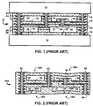
- FIG. 1 therein is shown a prior art multilayer ceramic structure or device 10 in an assembled condition in the top and bottom fixtures 12 and 14 of a hydraulic press.
- the multilayer ceramic device 10 has wide ceramic top and bottom layers 16 and 18 and wide ceramic intermediate layers 19 and 20. It should be understood that the horizontal width of the multilayer ceramic device 10 is being shown and that the ceramic layers 16, 18, 19, and 20 may have relatively long lengths compared to the widths and thicknesses shown.
- the multilayer ceramic device 10 has ceramic intermediate layers 22 and 24 which space apart the ceramic top layer 16 and the ceramic intermediate layer 19.
- the ceramic intermediate layers 26 and 28 space apart the ceramic intermediate layer 20 and the ceramic bottom layer 18.
- the ceramic intermediate layers generally have square or rectangular openings provided therein although serpentine openings are possible.
- the multilayer ceramic device 10 has channels 32, 34, 36, and 37 which are formed by the various ceramic layers. The width and heights of the channels are shown.
- the ceramic layer 16 defines the top of the chambers 32 and 34 while the ceramic intermediate layer 19 defines its bottom. If a single channel structure were being formed, the ceramic intermediate layer 19 could form the bottom of the structure.
- the intermediate layers 22 and 24 effectively define the sidewalls of the channels 32 and 34 and their height.
- the intermediate layer 19 and the intermediate layers 22 and 24, when assembled together as a subassembly can form what can be described as an enclosure layer.
- the enclosure layer and the ceramic top layer 16 define the chambers 32 and 34.
- a given ceramic intermediate layer, such as intermediate layer 22 could be formed as a single piece with an elongated, enclosed vertical opening in it which could act as a short channel or via.
- the ceramic bottom layer 18 is provided with orifices 38 and 39 which connect to the channels 36 and 37, respectively. These orifices 38 and 39 are particularly important when the multilayer ceramic device 10 is a molten alloy ejector since controlled droplets of molten metal will be ejected through the orifices 38 and 39.
- FIG. 2 therein is shown the prior art multilayer ceramic device 10A after being compressed between top and bottom fixtures 12 and 14, respectively, of a hydraulic press (not shown) at between 35 kg/cm 2 to 140 kg/cm 2 (500 psi to 2,000 psi) at approximately 75°C.
- the inward buckling of the ceramic top and bottom layers 16A and 18A which create detrimental non-planarities in the outside surfaces is shown.
- deformed orifices 38A and 39B which are a further drawback of the prior art. This problem is especially acute when the aspect ratio of the thickness of the top or bottom layer 16A or 18A to the width of the channel immediately adjacent is less than 1:1; i.e., if a top or bottom layer is thinner than the width of the channel.
- conductive material filled openings or vias 40, 42, 44, 46, and 48 which interconnect various levels of the multilayer ceramic device 10A.
- the openings for these conductive vias are generally formed by mechanical punching or laser ablation of holes into the various green, ceramic layers.
- the holes are subsequently filled with a metal fusible paste which will fuse with fusible paste in other via openings during the cofiring process, as will later be explained.
- fusible metal paste in the form of conductors 52, 54, 56, and 58 are laid down by a printing process onto the green layers to be subsequently fused into a solid conductor with the conductors in the conductive vias 40, 42, 44, 46, and 48 during the laminating and cofiring process. While not conductively connected to the other conductors or vias, the conductor 58 also fuses to the via 46.
- the various ceramic layers are processed by various machining steps for thick-film deposition of conductive materials and that the compression operation helps fuse the conductive materials and isolate those areas which are to be isolated.
- An example would be to isolate the via 46 and conductor 58 from the via 44 and the conductor 56.
- FIG. 3 therein is shown an embodiment of multilayer ceramic device 10B with ceramic top layer 16B, ceramic bottom layer 18B, and a subassembly or enclosure layer 66.
- the ceramic top layer 16B, the ceramic bottom layer 18B, and the enclosure layer 66 have been fired as individual parts.
- the areas where they will contact when assembled are coated with a bonding agent 70.
- the bonding agent can be a ceramic sintering material, an epoxy, a brazing material, or other material for bonding surfaces together.
- the other parts, which are the same as those in FIG. 2, have the same part numbers.
- FIG. 4 therein is shown an embodiment of multilayer ceramic device 10B in which the ceramic top and bottom layers 16B and 18B have been bonded to the enclosure layer 66.
- the vias 40, 42, 46, and 48 and the conductors 52, 54, 56, and 58 have been fired so that they are electrically and mechanically connected where desired.
- green ceramic layers are utilised.
- the green ceramic generally has sufficient rigidity that it is self-supporting.
- Green ceramic is used at this point because it is softer than fired ceramics and thus easier to process by normal manufacturing tools. For example, vias can easily be drilled or punched, and thick-film printing techniques can be used to lay down the conductive material itself. Similarly, other processes such as laser ablation and grinding are easily performed on green ceramics.
- the various ceramic layers are then aligned and then subject to compression using fixtures 12 and 14, shown in FIG. 1, in a hydraulic press and fired.
- the organic binder in the green ceramic sheets flows together under pressure during lamination.
- the organic binder is burnt out and the ceramic layers sinter into a monolithic ceramic device.
- the firing fuses the fusible metal paste to be electrically and mechanically connected where desired.
- the internal stresses in the ceramic top and bottom layers 16A and 18A show themselves by buckling the ceramic top and bottom layers 16A and 18A whenever the aspect ratio (of layer thickness to channel width is less than 1:1.
- the layers then are not planar and have irregular depressions on the top and bottom surfaces.
- This buckling in the multilayer ceramic device 10A may be to such an extent that the device is rendered unusable for mounting certain types of integrated circuits on the ceramic top layer 16 which requires flatness within 0.002 cm per cm (0.002 inch per inch).
- the channels 32, 34, 36, and 37 may be of such reduced size that fluid passing through the channels may be constricted to render the ceramic device 10A unable to perform the function for which it is intended.
- cooling fluid for cooling integrated circuits on the surfaces of the ceramic layers 16A and 18A may be reduced to the point that premature failure of the integrated circuit (not shown) could occur.
- a molten alloy for a molten alloy ejector would not provide solder to certain locations on a printed circuit board.
- the channels 32, 34, 36, and 37 may be of such reduced size that the friction of molten metal therein might be increased to the point where the magnetic fields of the Tsung Pan et al. patent, supra, may be insufficient to provide the necessary flow to provide the proper metered volume of molten metal.
- the shape of the green ceramic layers 16B, 18B, 19, and 20, as well as the intermediate layers 22, 24, 26, and 28, are stamped to shape with the via holes being punched in.
- the via holes would then be filled in with a metal paste and the same metal paste would be printed on the layer.
- the individual green layers would then be compressed individually to bring the metal paste level with the surface of the layers.
- the ceramic layers 16B and 18B After preparation of the green, ceramic layers, the ceramic layers 16B and 18B would be placed flat on a surface in a furnace and fired such that no internal stresses would be caused by either a laminating process or the force of gravity. This eliminates detrimental non-planarities and would leave the fired ceramic layers 16B and 18B totally planar, or flat within 0.002 cm per cm (0.002 inch per inch).
- the interior green layers and intermediate layers such as intermediate layers 22, 24, 26, and 28 with layers 19 and 20, are built up, and using inserts, are assembled, aligned, and subjected to compression and firing to create sub-assemblies or the enclosure layer 66.
- the channels 32, 34, 36, and 37 could be compressed with inserts in place to support the ceramic intermediate layers 19 and 20 while the enclosure layer 66 is formed. It is possible to control the desired green density of the sub-assembly such that the single and multiple layer laminates could be combined and laminated at a lower pressure. This pressure would be sufficient to achieve adhesion of the desired layers, but not great enough to significantly change the density of those areas under load.
- the enclosure layer 66 is bonded using bonding agent 70 to ceramic top and bottom layers 16B and 18B.
- This multiple lamination technique just described can be used to build up complex, multilayer ceramic devices which are made up of multiple multilayer ceramic structures. These structures could have multiple near surface channels and still have exceedingly flat outer surfaces.
- the bonding agents 70 include brazing materials such as brass, bronze, or silver alloys in a flux, vacuum-cured adhesives, epoxies, or ceramic sintering materials.
- the contacting areas of the already-fired ceramic layers would be metallized by a cofired tungsten with plated nickel.
- the contacting areas of the enclosure layer would then be coated with a brazing material such as Cusil, a copper-silver alloy. This allows each layer to be individually fired and assembled, or various portions to be fired, laminated, and fired as sub-assemblies, and then assembled as a complete structure or device.
- brazing techniques are well known to those skilled in the art.
- the ceramic layers 16B and 18B have previously been fired, they can be very thin, yet totally planar, when assembled into the final multilayer ceramic device 10.
Landscapes
- Engineering & Computer Science (AREA)
- Microelectronics & Electronic Packaging (AREA)
- Laminated Bodies (AREA)
- Production Of Multi-Layered Print Wiring Board (AREA)
- Insulating Bodies (AREA)
Applications Claiming Priority (2)
| Application Number | Priority Date | Filing Date | Title |
|---|---|---|---|
| US196939 | 1998-11-20 | ||
| US09/196,939 US6242075B1 (en) | 1998-11-20 | 1998-11-20 | Planar multilayer ceramic structures with near surface channels |
Publications (2)
| Publication Number | Publication Date |
|---|---|
| EP1003211A2 true EP1003211A2 (fr) | 2000-05-24 |
| EP1003211A3 EP1003211A3 (fr) | 2001-07-04 |
Family
ID=22727377
Family Applications (1)
| Application Number | Title | Priority Date | Filing Date |
|---|---|---|---|
| EP99309087A Withdrawn EP1003211A3 (fr) | 1998-11-20 | 1999-11-16 | Structure à multi-couche céramique |
Country Status (4)
| Country | Link |
|---|---|
| US (1) | US6242075B1 (fr) |
| EP (1) | EP1003211A3 (fr) |
| JP (1) | JP2000174439A (fr) |
| CN (1) | CN1150604C (fr) |
Cited By (1)
| Publication number | Priority date | Publication date | Assignee | Title |
|---|---|---|---|---|
| US9666647B2 (en) | 2014-03-27 | 2017-05-30 | Boe Technology Group Co., Ltd. | OLED display and method of manufacturing the same |
Families Citing this family (18)
| Publication number | Priority date | Publication date | Assignee | Title |
|---|---|---|---|---|
| US6060777A (en) * | 1998-07-21 | 2000-05-09 | Intel Corporation | Underside heat slug for ball grid array packages |
| US6490159B1 (en) * | 2000-09-06 | 2002-12-03 | Visteon Global Tech., Inc. | Electrical circuit board and method for making the same |
| US20040238099A1 (en) * | 2003-05-29 | 2004-12-02 | Milano Vincent J. | Economical method of manufacturing features in a ceramic circuit board |
| TW200735308A (en) * | 2005-12-23 | 2007-09-16 | Koninkl Philips Electronics Nv | On-chip interconnect-stack cooling using sacrificial interconnect segments |
| US8356410B2 (en) * | 2007-06-13 | 2013-01-22 | The Boeing Company | Heat pipe dissipating system and method |
| WO2009111874A1 (fr) * | 2008-03-11 | 2009-09-17 | The Royal Institution For The Advancement Of Learning/ Mcgiil University | Traitement au niveau tranche à basse température pour dispositifs mems |
| WO2011006101A2 (fr) * | 2009-07-10 | 2011-01-13 | Coolsilicon Llc | Dispositifs et procédés servant aux réservoirs de structures de refroidissement intra-puces |
| US8077460B1 (en) | 2010-07-19 | 2011-12-13 | Toyota Motor Engineering & Manufacturing North America, Inc. | Heat exchanger fluid distribution manifolds and power electronics modules incorporating the same |
| US8659896B2 (en) | 2010-09-13 | 2014-02-25 | Toyota Motor Engineering & Manufacturing North America, Inc. | Cooling apparatuses and power electronics modules |
| US8199505B2 (en) | 2010-09-13 | 2012-06-12 | Toyota Motor Engineering & Manufacturing Norh America, Inc. | Jet impingement heat exchanger apparatuses and power electronics modules |
| US8427832B2 (en) | 2011-01-05 | 2013-04-23 | Toyota Motor Engineering & Manufacturing North America, Inc. | Cold plate assemblies and power electronics modules |
| US8391008B2 (en) | 2011-02-17 | 2013-03-05 | Toyota Motor Engineering & Manufacturing North America, Inc. | Power electronics modules and power electronics module assemblies |
| US8482919B2 (en) | 2011-04-11 | 2013-07-09 | Toyota Motor Engineering & Manufacturing North America, Inc. | Power electronics card assemblies, power electronics modules, and power electronics devices |
| DE102012106244B4 (de) * | 2012-07-11 | 2020-02-20 | Rogers Germany Gmbh | Metall-Keramik-Substrat |
| US8643173B1 (en) | 2013-01-04 | 2014-02-04 | Toyota Motor Engineering & Manufacturing North America, Inc. | Cooling apparatuses and power electronics modules with single-phase and two-phase surface enhancement features |
| US9131631B2 (en) | 2013-08-08 | 2015-09-08 | Toyota Motor Engineering & Manufacturing North America, Inc. | Jet impingement cooling apparatuses having enhanced heat transfer assemblies |
| JP7282073B2 (ja) * | 2018-03-02 | 2023-05-26 | 株式会社村田製作所 | 多層セラミック基板及び多層セラミック基板の製造方法 |
| CN114701046B (zh) * | 2022-05-05 | 2024-01-26 | 鄂尔多斯应用技术学院 | 一种超高压陶瓷电容器的制备设备及制备方法 |
Citations (1)
| Publication number | Priority date | Publication date | Assignee | Title |
|---|---|---|---|---|
| US4859520A (en) * | 1985-02-26 | 1989-08-22 | Interconnexions Ceramiques | Monolithic substrate for an electronic power component and process for the production thereof |
Family Cites Families (19)
| Publication number | Priority date | Publication date | Assignee | Title |
|---|---|---|---|---|
| DE3329325A1 (de) * | 1982-09-03 | 1984-03-08 | Peter 2563 Ipsach Herren | Kuehlkoerper zur fluessigkeitskuehlung wenigstens eines elektrischen leistungselementes |
| US4504340A (en) * | 1983-07-26 | 1985-03-12 | International Business Machines Corporation | Material and process set for fabrication of molecular matrix print head |
| DE3402003A1 (de) * | 1984-01-21 | 1985-07-25 | Brown, Boveri & Cie Ag, 6800 Mannheim | Leistungshalbleitermodul |
| JPH064324B2 (ja) * | 1984-06-11 | 1994-01-19 | キヤノン株式会社 | 液体噴射記録ヘツド |
| US4833000A (en) * | 1986-10-31 | 1989-05-23 | Gte Laboratories Incorporated | Ceramic monolithic structure having an internal cavity contained therein and a method of preparing the same |
| JPH0714110B2 (ja) * | 1988-08-17 | 1995-02-15 | 株式会社村田製作所 | 多層セラミック基板 |
| DE3835794A1 (de) * | 1988-10-20 | 1990-04-26 | Siemens Ag | Verfahren zur herstellung einer strukturierten keramikfolie bzw. eines aus solchen folien aufgebauten keramikkoerpers |
| US5158912A (en) * | 1991-04-09 | 1992-10-27 | Digital Equipment Corporation | Integral heatsink semiconductor package |
| JPH05206341A (ja) * | 1991-10-11 | 1993-08-13 | W R Grace & Co | 開口流路のあるセラミツク基質 |
| JPH05104716A (ja) * | 1991-10-15 | 1993-04-27 | Matsushita Electric Ind Co Ltd | インクジエツトヘツド装置およびその製造方法 |
| US5199165A (en) | 1991-12-13 | 1993-04-06 | Hewlett-Packard Company | Heat pipe-electrical interconnect integration method for chip modules |
| JPH07142822A (ja) * | 1993-09-20 | 1995-06-02 | Fujitsu Ltd | 回路基板及びその製造方法 |
| JPH07117229A (ja) * | 1993-10-26 | 1995-05-09 | Brother Ind Ltd | インクジェットヘッド |
| US5538582A (en) * | 1994-09-14 | 1996-07-23 | International Business Machines Corporation | Method for forming cavities without using an insert |
| US5622588A (en) * | 1995-02-02 | 1997-04-22 | Hestia Technologies, Inc. | Methods of making multi-tier laminate substrates for electronic device packaging |
| RU2106943C1 (ru) | 1996-01-04 | 1998-03-20 | Хьюлетт-Паккард | Метатель капель жидкого припоя |
| US5779971A (en) | 1996-06-07 | 1998-07-14 | Hewlett-Packard Company | Solder jet printhead |
| US5870823A (en) * | 1996-11-27 | 1999-02-16 | International Business Machines Corporation | Method of forming a multilayer electronic packaging substrate with integral cooling channels |
| US5976286A (en) * | 1997-10-14 | 1999-11-02 | International Business Machines Corporation | Multi-density ceramic structure and process thereof |
-
1998
- 1998-11-20 US US09/196,939 patent/US6242075B1/en not_active Expired - Fee Related
-
1999
- 1999-08-20 CN CNB991179900A patent/CN1150604C/zh not_active Expired - Fee Related
- 1999-11-15 JP JP11324279A patent/JP2000174439A/ja active Pending
- 1999-11-16 EP EP99309087A patent/EP1003211A3/fr not_active Withdrawn
Patent Citations (1)
| Publication number | Priority date | Publication date | Assignee | Title |
|---|---|---|---|---|
| US4859520A (en) * | 1985-02-26 | 1989-08-22 | Interconnexions Ceramiques | Monolithic substrate for an electronic power component and process for the production thereof |
Cited By (1)
| Publication number | Priority date | Publication date | Assignee | Title |
|---|---|---|---|---|
| US9666647B2 (en) | 2014-03-27 | 2017-05-30 | Boe Technology Group Co., Ltd. | OLED display and method of manufacturing the same |
Also Published As
| Publication number | Publication date |
|---|---|
| CN1261026A (zh) | 2000-07-26 |
| EP1003211A3 (fr) | 2001-07-04 |
| CN1150604C (zh) | 2004-05-19 |
| US6242075B1 (en) | 2001-06-05 |
| JP2000174439A (ja) | 2000-06-23 |
Similar Documents
| Publication | Publication Date | Title |
|---|---|---|
| US6242075B1 (en) | Planar multilayer ceramic structures with near surface channels | |
| EP0108211B1 (fr) | Condensateurs "multi plaque" et leur procédé de fabrication | |
| KR100862537B1 (ko) | 세라믹 기판의 제조방법 및 비소성 세라믹 기판 | |
| KR100211852B1 (ko) | 전자회로기판 및 그 제조 방법 | |
| US4882212A (en) | Electronic packaging of components incorporating a ceramic-glass-metal composite | |
| KR100352780B1 (ko) | 다층 세라믹 기판 및 그의 제조방법 | |
| EP0244696B1 (fr) | Procédé de fabriquer un substrat multicouche en céramique comprenant des conducteurs métalliques solides non poreux | |
| US5024883A (en) | Electronic packaging of components incorporating a ceramic-glass-metal composite | |
| EP0932500B1 (fr) | Procede de controle des dimensions d'une cavite de plaquettes de circuit a couches multiples portees en cuisson et posees sur un support | |
| KR100200902B1 (ko) | 다층세라믹 소결체 및 그 제조방법 | |
| US4879156A (en) | Multilayered ceramic substrate having solid non-porous metal conductors | |
| US5798469A (en) | Non-sintering controlled pattern formation | |
| KR100521941B1 (ko) | 다층 세라믹 기판의 제조 방법 | |
| KR20040031680A (ko) | 전자 장치 및 그 제조 방법 | |
| US5276963A (en) | Process for obtaining side metallization and articles produced thereby | |
| US5876536A (en) | Method for the reduction of lateral shrinkage in multilayer circuit boards on a substrate | |
| US5302219A (en) | Method for obtaining via patterns in ceramic sheets | |
| KR100473773B1 (ko) | 다층 세라믹 기판 제조 방법 | |
| WO2003072325A1 (fr) | Procede pour fabriquer un substrat multicouche ceramique et corps multicouche composite cru | |
| EP0535711A2 (fr) | Procédé pour la fabrication d'un substrat céramique à multi-couche | |
| US20100038013A1 (en) | Method for manufacturing multilayer ceramic electronic device | |
| US6846375B2 (en) | Method of manufacturing multilayer ceramic wiring board and conductive paste for use | |
| US6709749B1 (en) | Method for the reduction of lateral shrinkage in multilayer circuit boards on a substrate | |
| EP0359416A2 (fr) | Circuits hybrides | |
| JP4089356B2 (ja) | 多層セラミック基板の製造方法 |
Legal Events
| Date | Code | Title | Description |
|---|---|---|---|
| PUAI | Public reference made under article 153(3) epc to a published international application that has entered the european phase |
Free format text: ORIGINAL CODE: 0009012 |
|
| AK | Designated contracting states |
Kind code of ref document: A2 Designated state(s): DE FR GB |
|
| AX | Request for extension of the european patent |
Free format text: AL;LT;LV;MK;RO;SI |
|
| RAP1 | Party data changed (applicant data changed or rights of an application transferred) |
Owner name: HEWLETT-PACKARD COMPANY, A DELAWARE CORPORATION |
|
| PUAL | Search report despatched |
Free format text: ORIGINAL CODE: 0009013 |
|
| AK | Designated contracting states |
Kind code of ref document: A3 Designated state(s): AT BE CH CY DE DK ES FI FR GB GR IE IT LI LU MC NL PT SE |
|
| AX | Request for extension of the european patent |
Free format text: AL;LT;LV;MK;RO;SI |
|
| RIC1 | Information provided on ipc code assigned before grant |
Free format text: 7H 01L 21/48 A, 7H 01L 21/50 B |
|
| 17P | Request for examination filed |
Effective date: 20011217 |
|
| AKX | Designation fees paid |
Free format text: DE FR GB |
|
| 17Q | First examination report despatched |
Effective date: 20040624 |
|
| STAA | Information on the status of an ep patent application or granted ep patent |
Free format text: STATUS: THE APPLICATION HAS BEEN WITHDRAWN |
|
| 18W | Application withdrawn |
Effective date: 20070423 |