EP1003358B1 - Verfahren zur Kontaktierung eines Bauelements und Schaltungsanordnung - Google Patents
Verfahren zur Kontaktierung eines Bauelements und Schaltungsanordnung Download PDFInfo
- Publication number
- EP1003358B1 EP1003358B1 EP99122724A EP99122724A EP1003358B1 EP 1003358 B1 EP1003358 B1 EP 1003358B1 EP 99122724 A EP99122724 A EP 99122724A EP 99122724 A EP99122724 A EP 99122724A EP 1003358 B1 EP1003358 B1 EP 1003358B1
- Authority
- EP
- European Patent Office
- Prior art keywords
- polymer
- soldered joint
- circuit arrangement
- arrangement according
- component
- Prior art date
- Legal status (The legal status is an assumption and is not a legal conclusion. Google has not performed a legal analysis and makes no representation as to the accuracy of the status listed.)
- Expired - Lifetime
Links
Images
Classifications
-
- H—ELECTRICITY
- H05—ELECTRIC TECHNIQUES NOT OTHERWISE PROVIDED FOR
- H05K—PRINTED CIRCUITS; CASINGS OR CONSTRUCTIONAL DETAILS OF ELECTRIC APPARATUS; MANUFACTURE OF ASSEMBLAGES OF ELECTRICAL COMPONENTS
- H05K3/00—Apparatus or processes for manufacturing printed circuits
- H05K3/30—Assembling printed circuits with electric components, e.g. with resistors
- H05K3/32—Assembling printed circuits with electric components, e.g. with resistors electrically connecting electric components or wires to printed circuits
- H05K3/34—Assembling printed circuits with electric components, e.g. with resistors electrically connecting electric components or wires to printed circuits by soldering
- H05K3/3447—Lead-in-hole components
-
- H—ELECTRICITY
- H05—ELECTRIC TECHNIQUES NOT OTHERWISE PROVIDED FOR
- H05K—PRINTED CIRCUITS; CASINGS OR CONSTRUCTIONAL DETAILS OF ELECTRIC APPARATUS; MANUFACTURE OF ASSEMBLAGES OF ELECTRICAL COMPONENTS
- H05K3/00—Apparatus or processes for manufacturing printed circuits
- H05K3/30—Assembling printed circuits with electric components, e.g. with resistors
- H05K3/32—Assembling printed circuits with electric components, e.g. with resistors electrically connecting electric components or wires to printed circuits
- H05K3/321—Assembling printed circuits with electric components, e.g. with resistors electrically connecting electric components or wires to printed circuits by conductive adhesives
-
- H—ELECTRICITY
- H05—ELECTRIC TECHNIQUES NOT OTHERWISE PROVIDED FOR
- H05K—PRINTED CIRCUITS; CASINGS OR CONSTRUCTIONAL DETAILS OF ELECTRIC APPARATUS; MANUFACTURE OF ASSEMBLAGES OF ELECTRICAL COMPONENTS
- H05K2201/00—Indexing scheme relating to printed circuits covered by H05K1/00
- H05K2201/10—Details of components or other objects attached to or integrated in a printed circuit board
- H05K2201/10007—Types of components
- H05K2201/1003—Non-printed inductor
-
- H—ELECTRICITY
- H05—ELECTRIC TECHNIQUES NOT OTHERWISE PROVIDED FOR
- H05K—PRINTED CIRCUITS; CASINGS OR CONSTRUCTIONAL DETAILS OF ELECTRIC APPARATUS; MANUFACTURE OF ASSEMBLAGES OF ELECTRICAL COMPONENTS
- H05K2201/00—Indexing scheme relating to printed circuits covered by H05K1/00
- H05K2201/10—Details of components or other objects attached to or integrated in a printed circuit board
- H05K2201/10007—Types of components
- H05K2201/10083—Electromechanical or electro-acoustic component, e.g. microphone
-
- H—ELECTRICITY
- H05—ELECTRIC TECHNIQUES NOT OTHERWISE PROVIDED FOR
- H05K—PRINTED CIRCUITS; CASINGS OR CONSTRUCTIONAL DETAILS OF ELECTRIC APPARATUS; MANUFACTURE OF ASSEMBLAGES OF ELECTRICAL COMPONENTS
- H05K2201/00—Indexing scheme relating to printed circuits covered by H05K1/00
- H05K2201/10—Details of components or other objects attached to or integrated in a printed circuit board
- H05K2201/10007—Types of components
- H05K2201/10166—Transistor
-
- H—ELECTRICITY
- H05—ELECTRIC TECHNIQUES NOT OTHERWISE PROVIDED FOR
- H05K—PRINTED CIRCUITS; CASINGS OR CONSTRUCTIONAL DETAILS OF ELECTRIC APPARATUS; MANUFACTURE OF ASSEMBLAGES OF ELECTRICAL COMPONENTS
- H05K2201/00—Indexing scheme relating to printed circuits covered by H05K1/00
- H05K2201/10—Details of components or other objects attached to or integrated in a printed circuit board
- H05K2201/10613—Details of electrical connections of non-printed components, e.g. special leads
- H05K2201/10954—Other details of electrical connections
- H05K2201/10977—Encapsulated connections
-
- H—ELECTRICITY
- H05—ELECTRIC TECHNIQUES NOT OTHERWISE PROVIDED FOR
- H05K—PRINTED CIRCUITS; CASINGS OR CONSTRUCTIONAL DETAILS OF ELECTRIC APPARATUS; MANUFACTURE OF ASSEMBLAGES OF ELECTRICAL COMPONENTS
- H05K2201/00—Indexing scheme relating to printed circuits covered by H05K1/00
- H05K2201/10—Details of components or other objects attached to or integrated in a printed circuit board
- H05K2201/10613—Details of electrical connections of non-printed components, e.g. special leads
- H05K2201/10954—Other details of electrical connections
- H05K2201/10992—Using different connection materials, e.g. different solders, for the same connection
Definitions
- the invention relates to a method for contacting a component according to The preamble of claim 1. It further relates to a circuit arrangement according to the preamble of claim 9.
- the machine is produced by wave soldering Soldering or soldering by repeated application of solder in the so-called Nachlöthabilit reinforced.
- the object of the invention is to overcome the disadvantages of the prior art remove.
- a method and a Circuit arrangement can be specified with which a contact loss thermally and mechanically loaded solder joints can be avoided.
- the method is provided that the solder joint covered after solidification of the solder alloy with a conductive polymer becomes.
- the inventive method can be relatively simple and with low Cost to perform. It is accessible to mass production.
- the polymer contains, preferably 75 to 85 % By weight, silver.
- Such a highly filled polymer has particularly good Contact properties.
- the polymer may have a density of 3.1 to 3.9 g / cm 3 . It is advantageous that the polymer has a glass transition temperature in the range of 35 to 45 ° C. It may be a synthetic resin, preferably an epoxy resin. A polymer with the aforementioned properties is particularly easy to process.
- the viscosity of the polymer set to 10 to 50 Pas. That ensures the required Flow properties for full coverage of the solder joint.
- the polymer can by means of a dispenser or a dispenser on the Solder be applied. This allows a cost-effective automated Process management.
- the polymer in such a way that it covers the solder joint over the entire area and except for one the solder joint surrounding edge region of the contact surface extends. That guarantees itself at a contact surface side breakage of the solder joint a particularly safe Contacting the component.
- solder joint is covered with a conductive polymer.
- the Contacting such a circuit is characterized by a high Reliability. Even if the solder joint breaks, the electrical remains Keep in touch.
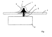
- the single FIGURE shows a schematic partial cross-sectional view of a Circuitry.
- a contact pin 1 of a component 2 passes through an opening 3 a circuit carrier 4.
- the circuit carrier 4 may be a circuit board or a chassis of a television or the like. Act.
- a solder joint 5 formed by a solder-miniscus connects in an electrically conductive manner a mounted on the circuit substrate 4 contact surface 5 with the Contact pin 2.
- the contact surface 5 may be part of a printed conductor be.
- the solder joint 5 is the entire surface with one of a conductive polymer. 7 covered layer covered. This, preferably about 81% by weight, silver containing polymer 7 extends in particular to the edge region of Contact surface 6, which is not covered by the soldering alloy.
- polymer 7 both one- and two-component conductive resins be used.
- Such polymers 7 are e.g. under the registered trademark Dotite from Fujikura Kasei Co., Ltd. or under the product name "PC 870007” available from Heraeus.
- the polymer 7 can by means of a dispenser on the solder joint to be secured. 5 be applied.
- the viscosity of the polymer 7 expediently set to 10 to 50 Pas.
- Robots are used to automate this process.
- the dispenser can advantageously be provided with a stirring device. Thereby, a segregation of the conductive polymer 7 during the Processing process avoided.
- the applied Temperatures of 50 to 70 ° C can be achieved by rinsing the soldered joint with hot air or generated by infrared radiation. They are above the Glass transition temperature of the polymer 7, which is about 35 ° C to 45 ° C.
Landscapes
- Engineering & Computer Science (AREA)
- Manufacturing & Machinery (AREA)
- Microelectronics & Electronic Packaging (AREA)
- Electric Connection Of Electric Components To Printed Circuits (AREA)
- Connections Effected By Soldering, Adhesion, Or Permanent Deformation (AREA)
- Coupling Device And Connection With Printed Circuit (AREA)
- Manufacturing Of Electrical Connectors (AREA)
Description
Durch die vorgenannten Maßnahmen wird zwar die Zeit bis zum Bruch der Lötstelle verlängert. Das Problem eines Kontaktverlusts durch den Bruch der Lötstelle wird jedoch nicht grundsätzlich beseitigt.
- 1
- Kontaktstift
- 2
- Bauelement
- 3
- Durchbruch
- 4
- Schaltungsträger
- 5
- Lötstelle
- 6
- Kontaktfläche
- 7
- Polymer
Claims (16)
- Verfahren zur Kontaktierung eines Bauelements (2), insbesondere eines Sperrwandlers, Leistungstransistors und dgl., wobei mindestens ein Kontaktelement (1) des Bauelements (2) mittels einer schmelzflüssigen Lotlegierung mit einer auf einem Schaltungsträger (4) vorgesehenen Kontaktfläche (6) unter Bildung einer Lötstelle (3) kontaktiert wird,
dadurch gekennzeichnet, dass die Lötstelle (5) nach der Erstarrung der Lötlegierung mit einem leitfähigen Polymer (7) überdeckt wird. - Verfahren nach Anspruch 1,
wobei das Polymer (7), vorzugsweise 75 - 85 Gew.%, Silber enthält. - Verfahren nach einem der vorhergehenden Ansprüche,
wobei das Polymer (7) eine Dichte von 3,1 bis 3,9 g/cm3 aufweist. - Verfahren nach einem der vorhergehenden Ansprüche,
wobei das Polymer (7) eine Glasumwandlungstemperatur im Bereich von 35 bis 45 °C hat. - Verfahren nach einem der vorhergehenden Ansprüche,
wobei das Polymer (7) ein Kunstharz, vorzugsweise ein Epoxid-Harz, ist. - Verfahren nach einem der vorhergehenden Ansprüche,
wobei die Viskosität des Polymers (7) auf 10 bis 50 Pas eingestellt wird. - Verfahren nach einem der vorhergehenden Ansprüche,
wobei das Polymer (7) mittels einer Spendeeinrichtung auf die Lötstelle (5) aufgebracht wird. - Verfahren nach einem der vorhergehenden Ansprüche,
wobei das Polymer (7) so aufgetragen wird, dass es die Lötstelle (5) vollflächig abdeckt und sich bis auf einen die Lötstelle (5) umgebenden Randbereich der Kontaktfläche (6) erstreckt. - Schaltungsanordnung, bei der mindestens ein Kontaktelement (1) des Bauelements (2), insbesondere eines Sperrwandlers, Leistungstransistors und dgl., mittels einer schmelzflüssigen Lotlegierung mit einer auf einem Schaltungsträger (4) vorgesehenen Kontaktfläche (6) unter Bildung einer Lötstelle (5) kontaktiert ist,
dadurch gekennzeichnet, dass die Lötstelle (5) mit einem leitfähigen Polymer (7) überdeckt ist. - Schaltungsanordnung nach Anspruch 9,
wobei das Polymer (7), vorzugsweise 75 - 85 Gew.%, Silber enthält. - Schaltungsanordnung nach einem der Ansprüche 9 oder 10,
wobei die Viskosität des Polymers (7) beim Aufbringen auf die Lötstelle (5) 10 bis 50 Pas beträgt. - Schaltungsanordnung nach einem der Ansprüche 9 bis 11,
wobei das Polymer (7) mittels einer Spendeeinrichtung auf die Lötstelle (5) aufbringbar ist. - Schaltungsanordnung nach einem der Ansprüche 9 bis 12,
wobei das Polymer (7) eine Dichte von 3,1 bis 3,9 g/cm3 aufweist. - Schaltungsanordnung nach einem der Ansprüche 9 bis 13,
wobei das Polymer (7) eine Glasumwandlungstemperatur im Bereich von 35 bis 45°C hat. - Schaltungsanordnung nach einem der Ansprüche 9 bis 14,
wobei das Polymer (7) ein Kunstharz, vorzugsweise ein Epoxid-Harz, ist. - Schaltungsanordnung nach einem der Ansprüche 9 bis 15,
wobei das Polymer (7) so aufgetragen ist, dass es die Lötstelle (5) vollflächig abdeckt und sich bis auf einen die Lötstelle (5) umgebenden Randbereich erstreckt.
Applications Claiming Priority (2)
| Application Number | Priority Date | Filing Date | Title |
|---|---|---|---|
| DE19853153A DE19853153C1 (de) | 1998-11-18 | 1998-11-18 | Verfahren zur Kontaktierung eines Bauelements und Schaltungsanordnung |
| DE19853153 | 1998-11-18 |
Publications (3)
| Publication Number | Publication Date |
|---|---|
| EP1003358A2 EP1003358A2 (de) | 2000-05-24 |
| EP1003358A3 EP1003358A3 (de) | 2002-02-20 |
| EP1003358B1 true EP1003358B1 (de) | 2005-06-01 |
Family
ID=7888196
Family Applications (1)
| Application Number | Title | Priority Date | Filing Date |
|---|---|---|---|
| EP99122724A Expired - Lifetime EP1003358B1 (de) | 1998-11-18 | 1999-11-16 | Verfahren zur Kontaktierung eines Bauelements und Schaltungsanordnung |
Country Status (4)
| Country | Link |
|---|---|
| EP (1) | EP1003358B1 (de) |
| AT (1) | ATE297109T1 (de) |
| DE (2) | DE19853153C1 (de) |
| ES (1) | ES2242344T3 (de) |
Families Citing this family (2)
| Publication number | Priority date | Publication date | Assignee | Title |
|---|---|---|---|---|
| DE102011086546A1 (de) * | 2011-11-17 | 2013-05-23 | Osram Opto Semiconductors Gmbh | Anordnung aus einem optoelektronischen bauelement und einer leiterplatte |
| DE102012207296A1 (de) * | 2012-05-02 | 2013-11-07 | Robert Bosch Gmbh | Elektrische Durchkontaktierung mit mechanischer Dämpfung |
Family Cites Families (3)
| Publication number | Priority date | Publication date | Assignee | Title |
|---|---|---|---|---|
| US3912852A (en) * | 1974-05-31 | 1975-10-14 | Westinghouse Electric Corp | Thin-film electrical circuit lead connection arrangement |
| US4300184A (en) * | 1979-07-11 | 1981-11-10 | Johnson Controls, Inc. | Conformal coating for electrical circuit assemblies |
| US5611884A (en) * | 1995-12-11 | 1997-03-18 | Dow Corning Corporation | Flip chip silicone pressure sensitive conductive adhesive |
-
1998
- 1998-11-18 DE DE19853153A patent/DE19853153C1/de not_active Expired - Fee Related
-
1999
- 1999-11-16 EP EP99122724A patent/EP1003358B1/de not_active Expired - Lifetime
- 1999-11-16 AT AT99122724T patent/ATE297109T1/de not_active IP Right Cessation
- 1999-11-16 DE DE59912114T patent/DE59912114D1/de not_active Expired - Fee Related
- 1999-11-16 ES ES99122724T patent/ES2242344T3/es not_active Expired - Lifetime
Also Published As
| Publication number | Publication date |
|---|---|
| EP1003358A3 (de) | 2002-02-20 |
| ES2242344T3 (es) | 2005-11-01 |
| DE19853153C1 (de) | 1999-10-07 |
| EP1003358A2 (de) | 2000-05-24 |
| DE59912114D1 (de) | 2005-07-07 |
| ATE297109T1 (de) | 2005-06-15 |
Similar Documents
| Publication | Publication Date | Title |
|---|---|---|
| DE3888895T2 (de) | Verfahren zum elektrischen Verbinden von integrierten Schaltungschips, eine Harzzusammensetzung für Podeste, und gemäss diesem Verfahren hergestellte Flüssigkristallanzeigevorrichtung. | |
| DE3782646T2 (de) | Vorrichtung und verfahren zur verbindung von schaltungspackungen. | |
| DE19826648B4 (de) | Schaltungsträger mit einer optischen Schicht und optoelektronisches Bauelement | |
| DE69312709T2 (de) | Lötperle auf schaltungsanordnung | |
| DE102010047646B4 (de) | Harz-versiegelte elektronische Steuervorrichtung und Verfahren zur Herstellung derselben | |
| DE19640058C2 (de) | Leiterplatte mit Zugentlastung für Anschluß-Kabel, Verfahren zu deren Herstellung und Verbindung sowie deren Verwendung | |
| DE69418420T2 (de) | Verfahren zum Anlöten eines elektrischen Kabels an eine Schaltungsplatte | |
| DE19652030B4 (de) | Verfahren zum Einkapseln eines Infrarotsendeempfängers | |
| DE19855389A1 (de) | Elektronische Vorrichtung | |
| DE10232788A1 (de) | Elektronisches Bauteil mit einem Halbleiterchip | |
| EP1003358B1 (de) | Verfahren zur Kontaktierung eines Bauelements und Schaltungsanordnung | |
| EP0489958B1 (de) | Leiterplatte für elektronische Steuergeräte und Verfahren zum Herstellen einer solchen Leiterplatte | |
| DE9308842U1 (de) | Elektrische Baugruppe | |
| DE10059808A1 (de) | Verfahren zur Verbindung einer integrierten Schaltung und einer flexiblen Schaltung | |
| DE3903615A1 (de) | Elektrische leiterplatte | |
| DE3731969C2 (de) | ||
| DE9007439U1 (de) | Leistungshalbleitermodul mit integrierter Ansteuerungs- und Fehlerschutzplatine | |
| DE10142472A1 (de) | Elektronisches Hochleistung- und Leistungsbauteil mit Ausgangskontaktstiften | |
| WO1998000865A1 (de) | Modul für ein elektrisches gerät | |
| EP0751562B1 (de) | Wärmeleite-Befestigung eines elektronischen Leistungsbauelementes auf einer Leiterplatte mit Kühlblech | |
| DE69511992T2 (de) | Halbleiteranordnung und Verfahren zur Herstellung | |
| DE102007014337B4 (de) | Verfahren zum Bestücken eines Kontaktierungselementes mit einem elektrischen Bauelement sowie ein Kontaktierungselement mit einem elektrischen Bauelement | |
| DE29619867U1 (de) | Elektrisches Schalt- und Steuergerät | |
| DE9313483U1 (de) | Vorrichtung zur Aufnahme | |
| DE60203855T2 (de) | Verfahren zum fixieren eines elektronischen teils |
Legal Events
| Date | Code | Title | Description |
|---|---|---|---|
| PUAI | Public reference made under article 153(3) epc to a published international application that has entered the european phase |
Free format text: ORIGINAL CODE: 0009012 |
|
| AK | Designated contracting states |
Kind code of ref document: A2 Designated state(s): AT BE CH CY DE DK ES FI FR GB GR IE IT LI LU MC NL PT SE |
|
| AX | Request for extension of the european patent |
Free format text: AL;LT;LV;MK;RO;SI |
|
| RAP1 | Party data changed (applicant data changed or rights of an application transferred) |
Owner name: GRUNDIG AKTIENGESELLSCHAFT |
|
| PUAL | Search report despatched |
Free format text: ORIGINAL CODE: 0009013 |
|
| AK | Designated contracting states |
Kind code of ref document: A3 Designated state(s): AT BE CH CY DE DK ES FI FR GB GR IE IT LI LU MC NL PT SE |
|
| AX | Request for extension of the european patent |
Free format text: AL;LT;LV;MK;RO;SI |
|
| 17P | Request for examination filed |
Effective date: 20020814 |
|
| AKX | Designation fees paid |
Free format text: AT BE CH CY DE DK ES FI FR GB GR IE IT LI LU MC NL PT SE |
|
| RAP1 | Party data changed (applicant data changed or rights of an application transferred) |
Owner name: GRUNDIG MULTIMEDIA B.V. |
|
| GRAP | Despatch of communication of intention to grant a patent |
Free format text: ORIGINAL CODE: EPIDOSNIGR1 |
|
| GRAS | Grant fee paid |
Free format text: ORIGINAL CODE: EPIDOSNIGR3 |
|
| GRAA | (expected) grant |
Free format text: ORIGINAL CODE: 0009210 |
|
| AK | Designated contracting states |
Kind code of ref document: B1 Designated state(s): AT BE CH CY DE DK ES FI FR GB GR IE IT LI LU MC NL PT SE |
|
| PG25 | Lapsed in a contracting state [announced via postgrant information from national office to epo] |
Ref country code: IE Free format text: LAPSE BECAUSE OF FAILURE TO SUBMIT A TRANSLATION OF THE DESCRIPTION OR TO PAY THE FEE WITHIN THE PRESCRIBED TIME-LIMIT Effective date: 20050601 Ref country code: FI Free format text: LAPSE BECAUSE OF FAILURE TO SUBMIT A TRANSLATION OF THE DESCRIPTION OR TO PAY THE FEE WITHIN THE PRESCRIBED TIME-LIMIT Effective date: 20050601 |
|
| REG | Reference to a national code |
Ref country code: GB Ref legal event code: FG4D Free format text: NOT ENGLISH |
|
| REG | Reference to a national code |
Ref country code: CH Ref legal event code: EP |
|
| REG | Reference to a national code |
Ref country code: IE Ref legal event code: FG4D Free format text: LANGUAGE OF EP DOCUMENT: GERMAN |
|
| REF | Corresponds to: |
Ref document number: 59912114 Country of ref document: DE Date of ref document: 20050707 Kind code of ref document: P |
|
| PG25 | Lapsed in a contracting state [announced via postgrant information from national office to epo] |
Ref country code: SE Free format text: LAPSE BECAUSE OF FAILURE TO SUBMIT A TRANSLATION OF THE DESCRIPTION OR TO PAY THE FEE WITHIN THE PRESCRIBED TIME-LIMIT Effective date: 20050901 Ref country code: GR Free format text: LAPSE BECAUSE OF FAILURE TO SUBMIT A TRANSLATION OF THE DESCRIPTION OR TO PAY THE FEE WITHIN THE PRESCRIBED TIME-LIMIT Effective date: 20050901 Ref country code: DK Free format text: LAPSE BECAUSE OF FAILURE TO SUBMIT A TRANSLATION OF THE DESCRIPTION OR TO PAY THE FEE WITHIN THE PRESCRIBED TIME-LIMIT Effective date: 20050901 |
|
| GBT | Gb: translation of ep patent filed (gb section 77(6)(a)/1977) |
Effective date: 20050831 |
|
| REG | Reference to a national code |
Ref country code: ES Ref legal event code: FG2A Ref document number: 2242344 Country of ref document: ES Kind code of ref document: T3 |
|
| PG25 | Lapsed in a contracting state [announced via postgrant information from national office to epo] |
Ref country code: PT Free format text: LAPSE BECAUSE OF FAILURE TO SUBMIT A TRANSLATION OF THE DESCRIPTION OR TO PAY THE FEE WITHIN THE PRESCRIBED TIME-LIMIT Effective date: 20051103 |
|
| PG25 | Lapsed in a contracting state [announced via postgrant information from national office to epo] |
Ref country code: CY Free format text: LAPSE BECAUSE OF FAILURE TO SUBMIT A TRANSLATION OF THE DESCRIPTION OR TO PAY THE FEE WITHIN THE PRESCRIBED TIME-LIMIT Effective date: 20051116 |
|
| PG25 | Lapsed in a contracting state [announced via postgrant information from national office to epo] |
Ref country code: MC Free format text: LAPSE BECAUSE OF NON-PAYMENT OF DUE FEES Effective date: 20051130 Ref country code: LU Free format text: LAPSE BECAUSE OF NON-PAYMENT OF DUE FEES Effective date: 20051130 Ref country code: LI Free format text: LAPSE BECAUSE OF NON-PAYMENT OF DUE FEES Effective date: 20051130 Ref country code: CH Free format text: LAPSE BECAUSE OF NON-PAYMENT OF DUE FEES Effective date: 20051130 Ref country code: BE Free format text: LAPSE BECAUSE OF NON-PAYMENT OF DUE FEES Effective date: 20051130 |
|
| REG | Reference to a national code |
Ref country code: IE Ref legal event code: FD4D |
|
| ET | Fr: translation filed | ||
| PLBE | No opposition filed within time limit |
Free format text: ORIGINAL CODE: 0009261 |
|
| STAA | Information on the status of an ep patent application or granted ep patent |
Free format text: STATUS: NO OPPOSITION FILED WITHIN TIME LIMIT |
|
| 26N | No opposition filed |
Effective date: 20060302 |
|
| REG | Reference to a national code |
Ref country code: CH Ref legal event code: PL |
|
| PGFP | Annual fee paid to national office [announced via postgrant information from national office to epo] |
Ref country code: GB Payment date: 20061017 Year of fee payment: 8 |
|
| PGFP | Annual fee paid to national office [announced via postgrant information from national office to epo] |
Ref country code: ES Payment date: 20061110 Year of fee payment: 8 |
|
| PGFP | Annual fee paid to national office [announced via postgrant information from national office to epo] |
Ref country code: AT Payment date: 20061124 Year of fee payment: 8 |
|
| PGFP | Annual fee paid to national office [announced via postgrant information from national office to epo] |
Ref country code: FR Payment date: 20061127 Year of fee payment: 8 |
|
| PGFP | Annual fee paid to national office [announced via postgrant information from national office to epo] |
Ref country code: NL Payment date: 20061130 Year of fee payment: 8 Ref country code: IT Payment date: 20061130 Year of fee payment: 8 |
|
| PGFP | Annual fee paid to national office [announced via postgrant information from national office to epo] |
Ref country code: DE Payment date: 20070108 Year of fee payment: 8 |
|
| BERE | Be: lapsed |
Owner name: GRUNDIG MULTIMEDIA B.V. Effective date: 20051130 |
|
| GBPC | Gb: european patent ceased through non-payment of renewal fee |
Effective date: 20071116 |
|
| NLV4 | Nl: lapsed or anulled due to non-payment of the annual fee |
Effective date: 20080601 |
|
| PG25 | Lapsed in a contracting state [announced via postgrant information from national office to epo] |
Ref country code: AT Free format text: LAPSE BECAUSE OF NON-PAYMENT OF DUE FEES Effective date: 20071116 |
|
| PG25 | Lapsed in a contracting state [announced via postgrant information from national office to epo] |
Ref country code: NL Free format text: LAPSE BECAUSE OF NON-PAYMENT OF DUE FEES Effective date: 20080601 Ref country code: DE Free format text: LAPSE BECAUSE OF NON-PAYMENT OF DUE FEES Effective date: 20080603 |
|
| REG | Reference to a national code |
Ref country code: FR Ref legal event code: ST Effective date: 20080930 |
|
| PG25 | Lapsed in a contracting state [announced via postgrant information from national office to epo] |
Ref country code: GB Free format text: LAPSE BECAUSE OF NON-PAYMENT OF DUE FEES Effective date: 20071116 |
|
| REG | Reference to a national code |
Ref country code: ES Ref legal event code: FD2A Effective date: 20071117 |
|
| PG25 | Lapsed in a contracting state [announced via postgrant information from national office to epo] |
Ref country code: FR Free format text: LAPSE BECAUSE OF NON-PAYMENT OF DUE FEES Effective date: 20071130 Ref country code: ES Free format text: LAPSE BECAUSE OF NON-PAYMENT OF DUE FEES Effective date: 20071117 |
|
| PG25 | Lapsed in a contracting state [announced via postgrant information from national office to epo] |
Ref country code: IT Free format text: LAPSE BECAUSE OF NON-PAYMENT OF DUE FEES Effective date: 20071116 |