EP1005069A2 - Plaquette semiconductrice et sa méthode de fabrication - Google Patents
Plaquette semiconductrice et sa méthode de fabrication Download PDFInfo
- Publication number
- EP1005069A2 EP1005069A2 EP99122057A EP99122057A EP1005069A2 EP 1005069 A2 EP1005069 A2 EP 1005069A2 EP 99122057 A EP99122057 A EP 99122057A EP 99122057 A EP99122057 A EP 99122057A EP 1005069 A2 EP1005069 A2 EP 1005069A2
- Authority
- EP
- European Patent Office
- Prior art keywords
- wafer
- polishing
- grinding
- mirror
- front surface
- Prior art date
- Legal status (The legal status is an assumption and is not a legal conclusion. Google has not performed a legal analysis and makes no representation as to the accuracy of the status listed.)
- Withdrawn
Links
Images


Classifications
-
- H—ELECTRICITY
- H10—SEMICONDUCTOR DEVICES; ELECTRIC SOLID-STATE DEVICES NOT OTHERWISE PROVIDED FOR
- H10P—GENERIC PROCESSES OR APPARATUS FOR THE MANUFACTURE OR TREATMENT OF DEVICES COVERED BY CLASS H10
- H10P52/00—Grinding, lapping or polishing of wafers, substrates or parts of devices
-
- H—ELECTRICITY
- H10—SEMICONDUCTOR DEVICES; ELECTRIC SOLID-STATE DEVICES NOT OTHERWISE PROVIDED FOR
- H10P—GENERIC PROCESSES OR APPARATUS FOR THE MANUFACTURE OR TREATMENT OF DEVICES COVERED BY CLASS H10
- H10P90/00—Preparation of wafers not covered by a single main group of this subclass, e.g. wafer reinforcement
- H10P90/12—Preparing bulk and homogeneous wafers
Definitions
- the present invention relates to a semiconductor wafer, and especially a method for fabrication of a single crystal silicon wafer.
- a conventional method for fabricating a semiconductor wafer comprises a slicing step to obtain wafers of a thin disc shape by slicing a single crystal silicon ingot pulled with a single crystal pulling apparatus; a coarse chamfering step to chamfer a peripheral edge portion of the sliced wafer in order to prevent cracking or breakage of the wafer; a lapping step to flatten both of the front surface and the back surface of the chamfered wafer; a cleaning or etching step to remove a remaining mechanical damage layer formed by the chamfering step and lapping step; and a mirror-polishing step to mirror-polish the front surface of the etched wafer.
- a step of surface-grinding the front surface or the both surfaces of the wafer there can be conducted by combination of a step of surface-grinding the front surface or the both surfaces of the wafer, a double side polishing step for polishing both surfaces of the surface-ground wafer, a finishing chamfering step to mirror-polish a peripheral edge portion of the wafer before and after the double side polishing step, the finishing polishing step to mirror-polish the wafer subjected to the double side polishing, and a cleaning step for removing a polishing agent remaining on the polished wafer and contaminant in order to improve cleanness.
- the surface-grinding step has been introduced to support the lapping process, since high flatness of the wafer cannot be achieved only by the lapping process when a diameter of the wafer is large, especially more than 300 mm.
- grinding striations formed at the most peripheral portion during surface-grinding of the front surface or the both surfaces of the wafer have a P-V value of about 0.2 to 0.1 ⁇ m and a striation interval of about 1 to 10 mm. Accordingly, the shape of the polishing cloth is copied (followed) to the shape of the grinding striations when it is subjected to double side polishing, so that grinding striations remain as micro roughness having a P-V value of about 30 to 50 nm, even after a finishing mirror-polishing step.
- the present invention has been accomplished to solve the above-mentioned conventional problems, and an object of the invention is to eliminate the grinding striations which remain on the front surface even when double side polishing and front surface finishing mirror-polishing are conducted after the above-mentioned conventional step of surface-grinding of the front surface or the both surfaces, to improve the quality of the front surface of the wafer, and to provide the semiconductor wafer having a proper quality in the back surface suitable for the device process, and a method for fabricating it.
- the present invention provides a semiconductor wafer obtained, at least, by removing a mechanical damage layer by etching both surfaces of the wafer, flattening one of the surfaces by a surface-grinding means, polishing both of the surfaces, and then subjecting a front surface of the wafer to a finishing mirror-polishing when defining the surface subjected to surface-grinding as a back surface of the wafer.
- the wafer is excellent in flatness on both surfaces, and condition of the surfaces is different from each other.
- the front surface is finished to be a mirror surface having no micro roughness formed during surface-grinding
- the wafer of the present invention When the wafer of the present invention is used, there are no grinding striations remaining on the front surface which are formed in the case of the conventional wafer fabricated by conducting lapping of the both surfaces, surface-grinding of the front surface or the both surfaces, double side polishing, and mirror-polishing. Furthermore, when the wafer of the present invention is chucked at the back surface thereof, there are no problems, which may be easily caused in a device process because of too good flatness of the back surface, such as indistinguishability of the front surface from the back surface, necessity of re-adjustment of sensing sensitivity, difficulty of chucking and releasing the wafer, and liabilities in a conveying line such as contamination.
- the grinding striations on the back surface are never transferred on the front surface in fabrication of the wafer of the present invention. Accordingly, it can be used in a process of highly integrated devices, productivity and yield of a device can be improved, and cost can be significantly reduced.
- the present invention also provides a method for fabricating a semiconductor wafer comprising at least slicing a wafer from a semiconductor ingot, lapping both surfaces of the wafer, removing a mechanical damage layer by etching treatment, flattening one of the surfaces by a surface-grinding means, polishing both of the surfaces, and then subjecting a front surface of the wafer to a finishing mirror-polishing when defining the surface subjected to surface-grinding as a back surface of the wafer.
- a wafer having high flatness can be easily fabricated at low cost, as compared with the conventional method comprising a double side lapping step, a step of grinding a front surface or both surfaces, a double side polishing step and a mirror-polishing step.
- a problem of grinding striations remaining on the surface which is one of disadvantages in the conventional method, can be solved, and a wafer having a front surface comprising a mirror surface without grinding striations and micro roughness and a back surface with desired grinding striations, can be fabricated easily and at low cost.
- the mirror edge polishing (mirror-polishing on chamfered edge) is conducted before or after the double side polishing step, defects such as cracking or breakage of the wafer can be prevented during polishing or in a device process.
- the mirror edge polishing is more effective, since it is conducted after the peripheral edge portion of the wafer is ground for coarse chamfering before the lapping step in order to prevent cracking or breakage of the wafer or the like during lapping and a surface-grinding.
- a stock removal of the wafer in the etching treatment can be minimal for removing the mechanical damage layer.
- a semiconductor wafer having the front surface which is a mirror surface with high flatness and high brightness and without micro roughness and the back surface having appropriate fine grinding striations can be fabricated easily and at low cost. Accordingly, when the wafer is chucked in a device process, the grinding striations on the back surface are never transferred on the front surface of the wafer of the present invention, and it can be used in a process of highly integrated devices, productivity and yield of a device can be improved in a device process, and cost can be significantly reduced.
- the inventors of the present invention have found that it is preferable to use a surface formed by lapping without grinding striations as a front surface, and to use the other surface with grinding striations easily remaining after surface-grinding as a back surface of the wafer, in order to fabricate a wafer wherein grinding striations are eliminated which remain on the front surface even when double side polishing and finishing mirror-polishing are conducted, after a conventional lapping step and a step of surface-grinding a front surface or both surfaces of the wafer described above, and wherein there is no damage or problem relating to the back surface condition formed in a device process, and thereby both quality of the front surface and condition of the back surface can be improved, and have completed the present invention by defining combination of each step such as a lapping step, a surface-grinding step, a polishing step and a mirror-polishing step, and various conditions thereof.
- Fig.1 (A) is a flow chart schematically showing a method of fabrication according to the present invention, and a surface condition of the wafer obtained in each step.
- the method of fabrication shown in Fig.1 (A) substantially comprises the following eight steps.
- a lapping apparatus is used at first.
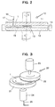
- Fig.2 shows an example of double side lapping apparatus used in the method of the present invention.
- a sliced wafer 1 is set between the lapping turn tables (the upper turn table 11 and the lower turn table 12) which are faced each other vertically.
- Lapping solution 17, which is generally a mixture of alumina or silicon carbide abrasive grains and glycerol is poured from a lapping solution nozzle 16 to a space between the lapping table and the wafer, in order to mechanically grind both surface of the wafer by rotating the lapping table for rubbing with pressing it on the wafer under pressure.
- the upper turn table 11 and the lower turn table 12 are rotated in opposite directions to each other.
- a center gear (sun gear) 13 is provided on the lower turn table 12, and an internal gear 14 is provided on the outer periphery of the lower turn table 12.
- Plural geared carriers 15 carrying plural wafers 1 each set in a wafer receiving hole, are interposed between the upper and lower lapping turn tables, and rotated and revolved between the center gear 13 and the internal gear 14. Thereby, the plural wafers 1 can be lapped at the same time under an adequate pressure applied by the upper turn table 11.
- the surface-grinding apparatus is an apparatus for grinding the wafer with a grinding wheel (grinding stone) after lapping and etching treatment to achieve higher flatness.
- a double side grinding apparatus for grinding both surfaces of the wafer at the same time, an infeed surface-grinding apparatus for grinding one surface or the like, are well known. In the method of the present invention, the latter is used.
- One example of the apparatus is shown in Fig.3.
- the wafer 1 lapped as described above is fixed on a rotatable suction plate 21 having a suction type fixing mechanism, and rotated by a suction plate driving motor 24, and the front surface or the back surface of the wafer can be ground with a cup-like grinding wheel 22 driven at high speed by a grinding wheel driving motor 23.
- a vacuum source (not shown) to which a vacuum pipe 25 is connected, is used.
- the double side polishing apparatus used in a double side polishing step is for mechanochemically polishing both surfaces of the wafer having stable thickness accuracy and flatness accuracy, subjected to the slicing step, the chamfering step, the flattening step and the etching step.
- a wafer 1 subjected to surface-grinding is set between polishing pads 33, 34 consisting of polyurethane foamed layer or the like adhered on the turn tables (the upper turn table 31 and the lower turn table 32) of the double side polishing apparatus 30 which are faced each other vertically.
- a polishing solution 39 generally consisting of polishing abrasive grains such as silica suspended in an alkali solution from a polishing solution nozzle 38 to a space between the polishing pad and the wafer, to mechanochemically polish both surfaces of the wafer by rotating them for rubbing under pressure.
- the upper turn table 31 and the lower turn table 32 are rotated in opposite directions to each other.
- a center gear (sun gear) 35 is provided on the lower turn table 32, and an internal gear 36 is provided on the outer periphery of the lower turn table 32.
- a plurality of geared carriers 37 carrying plural wafers 1 each set in a wafer receiving hole, are interposed between the upper and lower turn tables, and are rotated and revolved between the center gear 35 and the internal gear 36. Thereby, both surfaces of the plural wafers 1 can be polished at the same time under an adequate pressure applied by the upper turn table 31.
- the finishing mirror-polishing is conducted on one surface of the wafer in the method of the present invention.
- it is conducted through use of a single side polishing apparatus 40 shown in Fig.5 as follows.
- the back surface of the wafer 1 is fixed to a wafer holder 42 rotating with a holder shaft 47, using an adhesive such as wax which can be easily removed in the later cleaning step.
- a polishing cloth 45 consisting of polyurethane foamed layer or the like adhered on the turn table 41 is rotated with a turn table rotating shaft 46 at relative speed, with being loaded, to mirror-polish only front surface of the wafer mechanochemically.
- cleaning is conducted with, for example, SC-1 essentially comprising aqueous ammonia and hydrogen peroxide aqueous solution or SC-2 essentially comprising hydrochloric acid and hydrogen peroxide aqueous solution, in order to remove a polishing agent or the like adhered on the front surface of the wafer produced in the above-mentioned front surface finishing mirror-polishing step, and improve cleanness of the front and back surface.
- SC-1 essentially comprising aqueous ammonia and hydrogen peroxide aqueous solution
- SC-2 essentially comprising hydrochloric acid and hydrogen peroxide aqueous solution
- the mechanical damage layer formed on the front and back surface of the wafer formed in a flattening step according to a double side lapping method can be removed by chemical etching.
- An etching solution can be acid, alkali or the like.
- the flatness may be lowered depending on the kinds of the etching solution, a stirring condition of the etching solution during etching treatment, and progressing condition of the reaction.
- the flatness does not need to be cared so much since the flatness can be improved by the later surface grinding step.
- the inventors made experiments, and revealed that the best etching solution is an alkali solution such as a 45 to 50 % aqueous solution of sodium hydroxide or potassium hydroxide.
- the apparatuses described above namely, a double side lapping apparatus, a single side grinding apparatus, a double side polishing apparatus, a single side finishing mirror-polishing apparatus or the like were mainly used.
- the wafers having a diameter of 300 mm and a thickness of 975 ⁇ m were obtained as a starting material by a slicing step, and subjected to lapping, grinding, polishing and the like.
- the double side lapping step was conducted varying a stock removal in the range from 80 to 200 ⁇ m as a value of those of both surfaces put together.
- the etching step was conducted using an alkali solution or acid solution with a sufficient stock removal to remove a mechanical damage layer formed during lapping.
- the single side grinding was conducted using a grinding wheel such as a resin bond of #2000 to # 4000 with a stock removal of 10 to 20 ⁇ m.
- the double side polishing was conducted with a stock removal of 10 to 20 ⁇ m as a value of those of both surfaces put together, provided that the stock removal was determined so that the mechanical damage layer formed during a single side grinding can be removed.
- the double side polishing was conducted using a foamed urethane polishing cloth or a rigid urethane polishing pad (polishing cloth) as a polishing cloth.
- a polishing agent containing colloidal silica was used.
- the grinding striation is different from the mechanical damage, but is a shape formed on the surface by a grinding wheel, namely like undulation, which remains even after the double side polishing.
- the surface on which the grinding striations remained was determined as a back surface, the other surface, namely the front surface was subjected to a finishing mirror-polishing.
- the polishing was conducted with a stock removal of 1 to 2 ⁇ m by a copying polishing method wherein only the front surface of the wafer was mechanochemically polished to be a mirror surface.
- the wafers were evaluated, and revealed excellent as follows.
- P-V value shows a kind of microroughness, and is measured through use of NANOMETRO 330F (a laser displacement measuring apparatus manufactured by Kuroda Seikousha) in an area of 20 mm x 5 mm.
- the P-V value is a maximal difference between a peak and a valley.
- the wafer of the present invention were determined in the device step as for the problems in a device process, such as indistinguishability of the front surface from the back surface, necessity of re-adjustment of sensing sensitivity, difficulty of chucking and releasing the wafer, and liabilities in a conveying line such as contamination, which were easily caused in the case of the wafer wherein both surfaces were mirror-polished and had high flatness because flatness on the back surface was too good. Such problems were not caused in the wafer of the present invention.
- the present invention is not limited to the above-described embodiment.
- the above-described embodiment is a mere example, and those having the substantially same structure as that described in the appended claims and providing the similar action and effects are included in the scope of the present invention.
- the silicon wafer having a diameter of 300 mm (12 inches) was processed in the embodiment of the present invention.
- the present invention is applicable to the wafer having a large diameter such as 200 mm (8 inches) to 400 mm (16 inches) or more. Therefore, these modifications are included within the scope of the present invention.
- the method of the embodiment of the present invention comprises the steps shown in Fig.1 [A].
- the present invention is not limited to the steps shown there. There can be further added a heat treatment step, a cleaning step or the like, some of the steps can be omitted, and the sequence of the steps can be changed.
Landscapes
- Mechanical Treatment Of Semiconductor (AREA)
- Weting (AREA)
Applications Claiming Priority (2)
| Application Number | Priority Date | Filing Date | Title |
|---|---|---|---|
| JP33564298A JP3329288B2 (ja) | 1998-11-26 | 1998-11-26 | 半導体ウエーハおよびその製造方法 |
| JP33564298 | 1998-11-26 |
Publications (2)
| Publication Number | Publication Date |
|---|---|
| EP1005069A2 true EP1005069A2 (fr) | 2000-05-31 |
| EP1005069A3 EP1005069A3 (fr) | 2001-05-30 |
Family
ID=18290892
Family Applications (1)
| Application Number | Title | Priority Date | Filing Date |
|---|---|---|---|
| EP99122057A Withdrawn EP1005069A3 (fr) | 1998-11-26 | 1999-11-17 | Plaquette semiconductrice et sa méthode de fabrication |
Country Status (5)
| Country | Link |
|---|---|
| US (2) | US6352927B2 (fr) |
| EP (1) | EP1005069A3 (fr) |
| JP (1) | JP3329288B2 (fr) |
| KR (1) | KR20000035712A (fr) |
| TW (1) | TW494487B (fr) |
Cited By (2)
| Publication number | Priority date | Publication date | Assignee | Title |
|---|---|---|---|---|
| US7416962B2 (en) | 2002-08-30 | 2008-08-26 | Siltronic Corporation | Method for processing a semiconductor wafer including back side grinding |
| US7589023B2 (en) | 2000-04-24 | 2009-09-15 | Sumitomo Mitsubishi Silicon Corporation | Method of manufacturing semiconductor wafer |
Families Citing this family (31)
| Publication number | Priority date | Publication date | Assignee | Title |
|---|---|---|---|---|
| KR100750607B1 (ko) * | 1999-12-27 | 2007-08-20 | 신에쯔 한도타이 가부시키가이샤 | 웨이퍼 외주부의 가공능력 평가용 웨이퍼 및 웨이퍼외주부의 가공능력 평가방법 |
| JP4846915B2 (ja) * | 2000-03-29 | 2011-12-28 | 信越半導体株式会社 | 貼り合わせウェーハの製造方法 |
| US6722964B2 (en) * | 2000-04-04 | 2004-04-20 | Ebara Corporation | Polishing apparatus and method |
| US7582221B2 (en) * | 2000-10-26 | 2009-09-01 | Shin-Etsu Handotai Co., Ltd. | Wafer manufacturing method, polishing apparatus, and wafer |
| DE10060697B4 (de) * | 2000-12-07 | 2005-10-06 | Siltronic Ag | Doppelseiten-Polierverfahren mit reduzierter Kratzerrate und Vorrichtung zur Durchführung des Verfahrens |
| JP2002231665A (ja) * | 2001-02-06 | 2002-08-16 | Sumitomo Metal Ind Ltd | エピタキシャル膜付き半導体ウエーハの製造方法 |
| KR20030042858A (ko) * | 2001-11-26 | 2003-06-02 | 주식회사 실트론 | 실리콘 웨이퍼 연마 장치 및 제조 방법 |
| KR20030053084A (ko) * | 2001-12-22 | 2003-06-28 | 주식회사 실트론 | 실리콘 웨이퍼의 제조방법 |
| US6743722B2 (en) | 2002-01-29 | 2004-06-01 | Strasbaugh | Method of spin etching wafers with an alkali solution |
| US6796523B1 (en) | 2002-03-01 | 2004-09-28 | X-Spooler, Inc. | Wire winding machine with wire clamping and cutting assembly |
| JP4192482B2 (ja) * | 2002-03-22 | 2008-12-10 | 株式会社Sumco | シリコンウェーハの製造方法 |
| JP4093793B2 (ja) * | 2002-04-30 | 2008-06-04 | 信越半導体株式会社 | 半導体ウエーハの製造方法及びウエーハ |
| JP4521861B2 (ja) * | 2004-06-28 | 2010-08-11 | Sumco Techxiv株式会社 | 半導体ウェーハの薬液回収方法および装置 |
| US20060048798A1 (en) * | 2004-09-09 | 2006-03-09 | Honeywell International Inc. | Methods of cleaning optical substrates |
| JP4835069B2 (ja) * | 2005-08-17 | 2011-12-14 | 株式会社Sumco | シリコンウェーハの製造方法 |
| JP2008166805A (ja) * | 2006-12-29 | 2008-07-17 | Siltron Inc | 高平坦度シリコンウェハーの製造方法 |
| JP4947384B2 (ja) * | 2008-08-07 | 2012-06-06 | 大学共同利用機関法人 高エネルギー加速器研究機構 | 超伝導高周波加速空洞の製造方法 |
| DE102008045534B4 (de) * | 2008-09-03 | 2011-12-01 | Siltronic Ag | Verfahren zum Polieren einer Halbleiterscheibe |
| DE102009030297B3 (de) * | 2009-06-24 | 2011-01-20 | Siltronic Ag | Verfahren zum Polieren einer Halbleiterscheibe |
| US9064836B1 (en) * | 2010-08-09 | 2015-06-23 | Sandisk Semiconductor (Shanghai) Co., Ltd. | Extrinsic gettering on semiconductor devices |
| JP5479390B2 (ja) * | 2011-03-07 | 2014-04-23 | 信越半導体株式会社 | シリコンウェーハの製造方法 |
| US8860040B2 (en) | 2012-09-11 | 2014-10-14 | Dow Corning Corporation | High voltage power semiconductor devices on SiC |
| US9018639B2 (en) * | 2012-10-26 | 2015-04-28 | Dow Corning Corporation | Flat SiC semiconductor substrate |
| US9797064B2 (en) | 2013-02-05 | 2017-10-24 | Dow Corning Corporation | Method for growing a SiC crystal by vapor deposition onto a seed crystal provided on a support shelf which permits thermal expansion |
| US9738991B2 (en) | 2013-02-05 | 2017-08-22 | Dow Corning Corporation | Method for growing a SiC crystal by vapor deposition onto a seed crystal provided on a supporting shelf which permits thermal expansion |
| US9017804B2 (en) | 2013-02-05 | 2015-04-28 | Dow Corning Corporation | Method to reduce dislocations in SiC crystal growth |
| US8940614B2 (en) | 2013-03-15 | 2015-01-27 | Dow Corning Corporation | SiC substrate with SiC epitaxial film |
| US9279192B2 (en) | 2014-07-29 | 2016-03-08 | Dow Corning Corporation | Method for manufacturing SiC wafer fit for integration with power device manufacturing technology |
| CN107623028B (zh) * | 2016-07-13 | 2021-02-19 | 环球晶圆股份有限公司 | 半导体基板及其加工方法 |
| CN111482849A (zh) * | 2019-01-25 | 2020-08-04 | 东莞新科技术研究开发有限公司 | 一种减少晶圆厚度的方法 |
| CN115714082A (zh) * | 2022-10-31 | 2023-02-24 | 浙江丽水中欣晶圆半导体科技有限公司 | 提高硅片平坦度降低硅材料消耗的工艺 |
Family Cites Families (7)
| Publication number | Priority date | Publication date | Assignee | Title |
|---|---|---|---|---|
| US4144099A (en) * | 1977-10-31 | 1979-03-13 | International Business Machines Corporation | High performance silicon wafer and fabrication process |
| JPS5958827A (ja) * | 1982-09-28 | 1984-04-04 | Toshiba Corp | 半導体ウエ−ハ、半導体ウエ−ハの製造方法及び半導体ウエ−ハの製造装置 |
| EP0460437B1 (fr) * | 1990-05-18 | 1997-09-10 | Fujitsu Limited | Procédé pour fabriquer un substrat semi-conducteur et procédé pour fabriquer un dispositif semi-conducteur comportant ce substrat |
| JP2655975B2 (ja) * | 1992-09-18 | 1997-09-24 | 三菱マテリアル株式会社 | ウェーハ研磨装置 |
| JP2839801B2 (ja) * | 1992-09-18 | 1998-12-16 | 三菱マテリアル株式会社 | ウェーハの製造方法 |
| JP3317330B2 (ja) * | 1995-12-27 | 2002-08-26 | 信越半導体株式会社 | 半導体鏡面ウェーハの製造方法 |
| US5821166A (en) * | 1996-12-12 | 1998-10-13 | Komatsu Electronic Metals Co., Ltd. | Method of manufacturing semiconductor wafers |
-
1998
- 1998-11-26 JP JP33564298A patent/JP3329288B2/ja not_active Expired - Fee Related
-
1999
- 1999-11-17 EP EP99122057A patent/EP1005069A3/fr not_active Withdrawn
- 1999-11-19 TW TW088120265A patent/TW494487B/zh active
- 1999-11-22 US US09/447,309 patent/US6352927B2/en not_active Expired - Fee Related
- 1999-11-26 KR KR1019990052882A patent/KR20000035712A/ko not_active Abandoned
-
2001
- 2001-11-14 US US10/002,100 patent/US20020037650A1/en not_active Abandoned
Cited By (5)
| Publication number | Priority date | Publication date | Assignee | Title |
|---|---|---|---|---|
| US7589023B2 (en) | 2000-04-24 | 2009-09-15 | Sumitomo Mitsubishi Silicon Corporation | Method of manufacturing semiconductor wafer |
| DE10196115B4 (de) * | 2000-04-24 | 2011-06-16 | Sumitomo Mitsubishi Silicon Corp. | Verfahren zum Polieren eines Halbleiterwafers |
| US8283252B2 (en) | 2000-04-24 | 2012-10-09 | Sumitomo Mitsubishi Silicon Corporation | Method of manufacturing semiconductor wafer |
| US7416962B2 (en) | 2002-08-30 | 2008-08-26 | Siltronic Corporation | Method for processing a semiconductor wafer including back side grinding |
| DE10333810B4 (de) * | 2002-08-30 | 2010-02-11 | Siltronic Ag | Verfahren zum Bearbeiten eines Halbleiterwafers einschließlich Schleifen der Rückseite |
Also Published As
| Publication number | Publication date |
|---|---|
| KR20000035712A (ko) | 2000-06-26 |
| US6352927B2 (en) | 2002-03-05 |
| US20020037650A1 (en) | 2002-03-28 |
| US20010039119A1 (en) | 2001-11-08 |
| JP2000164542A (ja) | 2000-06-16 |
| EP1005069A3 (fr) | 2001-05-30 |
| JP3329288B2 (ja) | 2002-09-30 |
| TW494487B (en) | 2002-07-11 |
Similar Documents
| Publication | Publication Date | Title |
|---|---|---|
| US6352927B2 (en) | Semiconductor wafer and method for fabrication thereof | |
| JP3664593B2 (ja) | 半導体ウエーハおよびその製造方法 | |
| EP1808887B1 (fr) | Procede de production de tranche a semi-conducteurs | |
| US6214704B1 (en) | Method of processing semiconductor wafers to build in back surface damage | |
| EP2048701A2 (fr) | Suppression de bordure d'une tranche de transfert de silicium sur isolant | |
| US6753256B2 (en) | Method of manufacturing semiconductor wafer | |
| JP3328193B2 (ja) | 半導体ウエーハの製造方法 | |
| CN104350583A (zh) | 半导体晶片的制造方法 | |
| US5643405A (en) | Method for polishing a semiconductor substrate | |
| JP3828176B2 (ja) | 半導体ウェハの製造方法 | |
| US6465328B1 (en) | Semiconductor wafer manufacturing method | |
| JP2004087521A (ja) | 片面鏡面ウェーハおよびその製造方法 | |
| JP4224871B2 (ja) | 半導体基板の製造方法 | |
| JP3336191B2 (ja) | 半導体ウェ−ハの製造方法 | |
| JP2002025950A (ja) | 半導体ウェーハの製造方法 | |
| JP2003062740A (ja) | 鏡面ウェーハの製造方法 | |
| JP3399179B2 (ja) | ウェーハの加工方法 | |
| JP4154683B2 (ja) | 高平坦度裏面梨地ウェーハの製造方法および該製造方法に用いられる表面研削裏面ラップ装置 | |
| JP3131968B2 (ja) | 半導体シリコンウェーハの製造方法 | |
| JP2004319717A (ja) | 半導体ウェーハの製造方法 | |
| JP3596405B2 (ja) | 半導体ウェーハの製造方法 | |
| JP2003133264A (ja) | 鏡面ウエーハの製造方法 | |
| JP2001102340A (ja) | 半導体ウェーハの製造方法 | |
| JP2002334854A (ja) | 半導体装置の製造方法 |
Legal Events
| Date | Code | Title | Description |
|---|---|---|---|
| PUAI | Public reference made under article 153(3) epc to a published international application that has entered the european phase |
Free format text: ORIGINAL CODE: 0009012 |
|
| AK | Designated contracting states |
Kind code of ref document: A2 Designated state(s): DE GB |
|
| AX | Request for extension of the european patent |
Free format text: AL;LT;LV;MK;RO;SI |
|
| PUAL | Search report despatched |
Free format text: ORIGINAL CODE: 0009013 |
|
| AK | Designated contracting states |
Kind code of ref document: A3 Designated state(s): AT BE CH CY DE DK ES FI FR GB GR IE IT LI LU MC NL PT SE |
|
| AX | Request for extension of the european patent |
Free format text: AL;LT;LV;MK;RO;SI |
|
| RIC1 | Information provided on ipc code assigned before grant |
Free format text: 7H 01L 21/302 A, 7H 01L 21/304 B |
|
| 17P | Request for examination filed |
Effective date: 20010802 |
|
| AKX | Designation fees paid |
Free format text: DE GB |
|
| STAA | Information on the status of an ep patent application or granted ep patent |
Free format text: STATUS: THE APPLICATION IS DEEMED TO BE WITHDRAWN |
|
| 18D | Application deemed to be withdrawn |
Effective date: 20060530 |