EP1005170A1 - Flash Analog-Digitalwandler - Google Patents
Flash Analog-Digitalwandler Download PDFInfo
- Publication number
- EP1005170A1 EP1005170A1 EP98830712A EP98830712A EP1005170A1 EP 1005170 A1 EP1005170 A1 EP 1005170A1 EP 98830712 A EP98830712 A EP 98830712A EP 98830712 A EP98830712 A EP 98830712A EP 1005170 A1 EP1005170 A1 EP 1005170A1
- Authority
- EP
- European Patent Office
- Prior art keywords
- compi
- input
- bank
- output
- comparators
- Prior art date
- Legal status (The legal status is an assumption and is not a legal conclusion. Google has not performed a legal analysis and makes no representation as to the accuracy of the status listed.)
- Granted
Links
Images

Classifications
-
- H—ELECTRICITY
- H03—ELECTRONIC CIRCUITRY
- H03M—CODING; DECODING; CODE CONVERSION IN GENERAL
- H03M1/00—Analogue/digital conversion; Digital/analogue conversion
- H03M1/06—Continuously compensating for, or preventing, undesired influence of physical parameters
- H03M1/08—Continuously compensating for, or preventing, undesired influence of physical parameters of noise
- H03M1/0809—Continuously compensating for, or preventing, undesired influence of physical parameters of noise of bubble errors, i.e. irregularities in thermometer codes
-
- H—ELECTRICITY
- H03—ELECTRONIC CIRCUITRY
- H03M—CODING; DECODING; CODE CONVERSION IN GENERAL
- H03M1/00—Analogue/digital conversion; Digital/analogue conversion
- H03M1/12—Analogue/digital converters
- H03M1/34—Analogue value compared with reference values
- H03M1/36—Analogue value compared with reference values simultaneously only, i.e. parallel type
- H03M1/361—Analogue value compared with reference values simultaneously only, i.e. parallel type having a separate comparator and reference value for each quantisation level, i.e. full flash converter type
- H03M1/362—Analogue value compared with reference values simultaneously only, i.e. parallel type having a separate comparator and reference value for each quantisation level, i.e. full flash converter type the reference values being generated by a resistive voltage divider
- H03M1/365—Analogue value compared with reference values simultaneously only, i.e. parallel type having a separate comparator and reference value for each quantisation level, i.e. full flash converter type the reference values being generated by a resistive voltage divider the voltage divider being a single resistor string
Definitions
- the invention relates to signal processing systems, and more in particular to an analog/digital converter capable to output a thermometric digital code.
- the metastability errors may increase in number by several orders of magnitude upon increasing the clock frequency and/or decreasing the supply voltage.
- the enhancement of the performance of comparators employed in a converter is an approach that ceases to be effective when operating at the technological limits of integration and of minimization of the silicon requirement and/or of power consumption.
- the proposed techniques consist in introducing latch arrays in cascade (pipelining) of the comparators' outputs in order to increase the resolution time of the comparators.
- the pipelining technique while being capable to decisively reducing the number of errors, determines a conspicuous increment of the circuital complexity, that is, of the required silicon area and of the current absorption. Moreover, this approach implies a strict correlation between the increment of the complexity of the pipelining circuits downstream of the array of comparators and their performance in terms of their ability of reducing the number of errors.
- the output dynamic of the comparators may be of a few thermal potentials thereby the margin of noise reduction that may be obtained by implementing a common mode circuit, according to the technique suggested in the above cited article, is practically rather reduced.
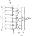
- the flash ADC of the invention comprises an array or bank of comparators (COMPi) having a differential output and generating a thermometric code and a bank of three-input (A, B, C) logic NOR gates (NORj), and a passive interface constituted by voltage dividers (Ra-Rb).
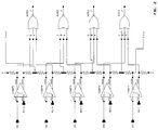
- Each voltage divider is connected between the noninverted output (out_p) of a respective comparator (COMPi-1) and the inverted output (out_n) of the comparator of higher order (COMPi).
- the respective NOR gate has a first input (A) coupled to the inverted output (out_n) of the respective comparator (COMPi-1), a second input (B) coupled to the noninverted output (out_p) of the comparator of higher order (COMPi) and a third input (C) coupled to a intermediate tap of the voltage divider connected between the noninverted output (out_p) of the respective comparator (COMPi-1) and the inverted output (out_n) of the comparator of higher order (COMPi).
- the passive interface constituted by the plurality of voltage dividers (Ra-Rb) decisively increases the immunity to common mode disturbances and noise without sensibly increasing neither the area requirement nor the power consumption.
- Fig. 1 shows the architecture of a flash ADC in which the bank of comparators COMPi supply a thermometric code and the bank of latches NORj outputs only a "1" and all "0s" to the NOR plane of a decoding PLA which outputs an N bit word or digital datum corresponding to the sampled analog value Vin.
- Fig. 2 shows the detail of the flash ADC circuit of Fig. 1, modified according to the present invention.
- the common mode input of the NOR gate coupled to the outputs of the two consecutive comparators may be considered ideally equal to the output common mode of the two comparators, in this case the two comparators are not metastable.
- Fig. 3 shows a suitable circuit for each three-input logic NOR gate, usable in the flash analog-to-digital converter of the invention.
Landscapes
- Engineering & Computer Science (AREA)
- Theoretical Computer Science (AREA)
- Analogue/Digital Conversion (AREA)
Priority Applications (4)
| Application Number | Priority Date | Filing Date | Title |
|---|---|---|---|
| DE69803856T DE69803856D1 (de) | 1998-11-27 | 1998-11-27 | Flash Analog-Digitalwandler |
| EP98830712A EP1005170B1 (de) | 1998-11-27 | 1998-11-27 | Flash Analog-Digitalwandler |
| JP11330072A JP2000174626A (ja) | 1998-11-27 | 1999-11-19 | フラッシュアナログ・デジタル変換器 |
| US09/447,065 US6346905B1 (en) | 1998-11-27 | 1999-11-22 | Analog-to-digital flash converter for generating a thermometric digital code |
Applications Claiming Priority (1)
| Application Number | Priority Date | Filing Date | Title |
|---|---|---|---|
| EP98830712A EP1005170B1 (de) | 1998-11-27 | 1998-11-27 | Flash Analog-Digitalwandler |
Publications (2)
| Publication Number | Publication Date |
|---|---|
| EP1005170A1 true EP1005170A1 (de) | 2000-05-31 |
| EP1005170B1 EP1005170B1 (de) | 2002-02-13 |
Family
ID=8236901
Family Applications (1)
| Application Number | Title | Priority Date | Filing Date |
|---|---|---|---|
| EP98830712A Expired - Lifetime EP1005170B1 (de) | 1998-11-27 | 1998-11-27 | Flash Analog-Digitalwandler |
Country Status (4)
| Country | Link |
|---|---|
| US (1) | US6346905B1 (de) |
| EP (1) | EP1005170B1 (de) |
| JP (1) | JP2000174626A (de) |
| DE (1) | DE69803856D1 (de) |
Cited By (1)
| Publication number | Priority date | Publication date | Assignee | Title |
|---|---|---|---|---|
| US6346905B1 (en) | 1998-11-27 | 2002-02-12 | Stmicroelectronics S.R.L. | Analog-to-digital flash converter for generating a thermometric digital code |
Families Citing this family (15)
| Publication number | Priority date | Publication date | Assignee | Title |
|---|---|---|---|---|
| DK1487485T3 (da) * | 2002-03-19 | 2011-03-14 | Powderject Res Ltd | Imidazoquinolinadjuvanser til DNA-vacciner |
| KR100500441B1 (ko) * | 2002-10-22 | 2005-07-14 | 삼성전자주식회사 | 플래쉬 방식 아날로그 디지털 변환방법 및 회로 |
| KR100462888B1 (ko) * | 2002-10-24 | 2004-12-17 | 삼성전자주식회사 | 플래쉬 아날로그 디지털 변환회로의 비교기 어레이의배치방법 |
| US7521960B2 (en) * | 2003-07-31 | 2009-04-21 | Actel Corporation | Integrated circuit including programmable logic and external-device chip-enable override control |
| US7170315B2 (en) | 2003-07-31 | 2007-01-30 | Actel Corporation | Programmable system on a chip |
| US7138824B1 (en) * | 2004-05-10 | 2006-11-21 | Actel Corporation | Integrated multi-function analog circuit including voltage, current, and temperature monitor and gate-driver circuit blocks |
| US7099189B1 (en) | 2004-10-05 | 2006-08-29 | Actel Corporation | SRAM cell controlled by non-volatile memory cell |
| US7116181B2 (en) * | 2004-12-21 | 2006-10-03 | Actel Corporation | Voltage- and temperature-compensated RC oscillator circuit |
| US7119398B1 (en) * | 2004-12-22 | 2006-10-10 | Actel Corporation | Power-up and power-down circuit for system-on-a-chip integrated circuit |
| US7446378B2 (en) * | 2004-12-29 | 2008-11-04 | Actel Corporation | ESD protection structure for I/O pad subject to both positive and negative voltages |
| US7623051B2 (en) * | 2008-04-29 | 2009-11-24 | Analog Devices, Inc. | Metastability error reduction in signal converter systems |
| US8416106B2 (en) * | 2011-04-20 | 2013-04-09 | Fujitsu Limited | Calibration scheme for resolution scaling, power scaling, variable input swing and comparator offset cancellation for flash ADCs |
| GB2520232A (en) | 2013-08-06 | 2015-05-20 | Univ Edinburgh | Multiple Event Time to Digital Converter |
| US9502458B2 (en) | 2015-03-10 | 2016-11-22 | Stmicroelectronics (Research & Development) Limited | Circuit for generating direct timing histogram data in response to photon detection |
| US9722623B1 (en) * | 2016-12-19 | 2017-08-01 | Stmicroelectronics International N.V. | Analog-to-digital converter with dynamic element matching |
Citations (3)
| Publication number | Priority date | Publication date | Assignee | Title |
|---|---|---|---|---|
| US4733220A (en) * | 1985-10-04 | 1988-03-22 | Tektronix, Inc. | Thermometer-to-adjacent bindary encoder |
| US5029305A (en) * | 1988-12-21 | 1991-07-02 | Texas Instruments Incorporated | Method and apparatus for error correction in thermometer code arrays |
| US5272461A (en) * | 1990-02-15 | 1993-12-21 | Siemens Aktiengesellschaft | Coding circuit |
Family Cites Families (5)
| Publication number | Priority date | Publication date | Assignee | Title |
|---|---|---|---|---|
| GB9205727D0 (en) * | 1992-03-16 | 1992-04-29 | Sarnoff David Res Center | Averaging,flash analog to digital converter |
| US6225937B1 (en) * | 1996-05-24 | 2001-05-01 | Lockheed-Martin Ir Imaging Systems, Inc. | Metastability resolved monolithic analog-to-digital converter |
| US5808573A (en) * | 1996-08-01 | 1998-09-15 | Nec Electronics Incorporated | Methods and structure for sampled-data timing recovery with reduced complexity and latency |
| EP1005170B1 (de) | 1998-11-27 | 2002-02-13 | STMicroelectronics S.r.l. | Flash Analog-Digitalwandler |
| US6222476B1 (en) * | 1999-08-30 | 2001-04-24 | Lsi Logic Corporation | Architecture to reduce errors due to metastability in analog to digital converters |
-
1998
- 1998-11-27 EP EP98830712A patent/EP1005170B1/de not_active Expired - Lifetime
- 1998-11-27 DE DE69803856T patent/DE69803856D1/de not_active Expired - Lifetime
-
1999
- 1999-11-19 JP JP11330072A patent/JP2000174626A/ja active Pending
- 1999-11-22 US US09/447,065 patent/US6346905B1/en not_active Expired - Lifetime
Patent Citations (3)
| Publication number | Priority date | Publication date | Assignee | Title |
|---|---|---|---|---|
| US4733220A (en) * | 1985-10-04 | 1988-03-22 | Tektronix, Inc. | Thermometer-to-adjacent bindary encoder |
| US5029305A (en) * | 1988-12-21 | 1991-07-02 | Texas Instruments Incorporated | Method and apparatus for error correction in thermometer code arrays |
| US5272461A (en) * | 1990-02-15 | 1993-12-21 | Siemens Aktiengesellschaft | Coding circuit |
Cited By (1)
| Publication number | Priority date | Publication date | Assignee | Title |
|---|---|---|---|---|
| US6346905B1 (en) | 1998-11-27 | 2002-02-12 | Stmicroelectronics S.R.L. | Analog-to-digital flash converter for generating a thermometric digital code |
Also Published As
| Publication number | Publication date |
|---|---|
| US6346905B1 (en) | 2002-02-12 |
| JP2000174626A (ja) | 2000-06-23 |
| EP1005170B1 (de) | 2002-02-13 |
| DE69803856D1 (de) | 2002-03-21 |
Similar Documents
| Publication | Publication Date | Title |
|---|---|---|
| EP1005170B1 (de) | Flash Analog-Digitalwandler | |
| US8482449B1 (en) | Analog-to-digital converter with metastability detector | |
| US4897657A (en) | Analog-to-digital converter having error detection and correction | |
| US8957802B1 (en) | Metastability error detection and correction system and method for successive approximation analog-to-digital converters | |
| US8198921B2 (en) | Dynamic comparator with background offset calibration | |
| US6232908B1 (en) | A/D converter having a dynamic encoder | |
| US20070290915A1 (en) | Pipeline A/D converter conterting analog signal to digital signal | |
| US20100045503A1 (en) | Pulse phase difference detecting circuit and A/D converter using the same | |
| EP0120424B1 (de) | Parallelvergleichstyp Analog-Digitalwandler | |
| Ito et al. | A 10 bit 20 MS/s 3 V supply CMOS A/D converter | |
| US5194867A (en) | Flash analog-to-digital converter employing least significant bit-representative comparative reference voltage | |
| US5012246A (en) | BiCMOS analog-to-digital converter with minimized metastability | |
| US6388602B1 (en) | Bubble and meta-stability error immune gray-code encoder for high-speed A/D converters | |
| US6222476B1 (en) | Architecture to reduce errors due to metastability in analog to digital converters | |
| US5623265A (en) | Flash analog-to-digital converter and method of operation | |
| Cai et al. | A 25GS/s 6b TI binary search ADC with soft-decision selection in 65nm CMOS | |
| Ghoshal et al. | A bit swap logic (BSL) based bubble error correction (BEC) method for flash ADCs | |
| Patil et al. | Low power dynamic comparator for 4—bit Flash ADC | |
| US9357151B1 (en) | Shared counter circuit with low-voltage signal output for a column-parallel single slope ADC | |
| EP1150433A2 (de) | Analog-Digital-Wandler nach dem Parallelverfahren | |
| US7327292B2 (en) | Bubble error rejecter in data converter | |
| Kaplan et al. | Real-time digital error correction for flash analog-to-digital converter | |
| JP2585578B2 (ja) | Ad変換器 | |
| US10763880B1 (en) | Analog to digital converter | |
| US5272461A (en) | Coding circuit |
Legal Events
| Date | Code | Title | Description |
|---|---|---|---|
| PUAI | Public reference made under article 153(3) epc to a published international application that has entered the european phase |
Free format text: ORIGINAL CODE: 0009012 |
|
| AK | Designated contracting states |
Kind code of ref document: A1 Designated state(s): DE FR GB IT |
|
| AX | Request for extension of the european patent |
Free format text: AL;LT;LV;MK;RO;SI |
|
| 17P | Request for examination filed |
Effective date: 20000529 |
|
| AKX | Designation fees paid |
Free format text: DE FR GB IT |
|
| GRAG | Despatch of communication of intention to grant |
Free format text: ORIGINAL CODE: EPIDOS AGRA |
|
| 17Q | First examination report despatched |
Effective date: 20010409 |
|
| GRAG | Despatch of communication of intention to grant |
Free format text: ORIGINAL CODE: EPIDOS AGRA |
|
| GRAH | Despatch of communication of intention to grant a patent |
Free format text: ORIGINAL CODE: EPIDOS IGRA |
|
| GRAH | Despatch of communication of intention to grant a patent |
Free format text: ORIGINAL CODE: EPIDOS IGRA |
|
| GRAA | (expected) grant |
Free format text: ORIGINAL CODE: 0009210 |
|
| REG | Reference to a national code |
Ref country code: GB Ref legal event code: IF02 |
|
| AK | Designated contracting states |
Kind code of ref document: B1 Designated state(s): DE FR GB IT |
|
| PG25 | Lapsed in a contracting state [announced via postgrant information from national office to epo] |
Ref country code: FR Free format text: LAPSE BECAUSE OF FAILURE TO SUBMIT A TRANSLATION OF THE DESCRIPTION OR TO PAY THE FEE WITHIN THE PRESCRIBED TIME-LIMIT Effective date: 20020213 |
|
| REF | Corresponds to: |
Ref document number: 69803856 Country of ref document: DE Date of ref document: 20020321 |
|
| PG25 | Lapsed in a contracting state [announced via postgrant information from national office to epo] |
Ref country code: DE Free format text: LAPSE BECAUSE OF FAILURE TO SUBMIT A TRANSLATION OF THE DESCRIPTION OR TO PAY THE FEE WITHIN THE PRESCRIBED TIME-LIMIT Effective date: 20020514 |
|
| EN | Fr: translation not filed | ||
| PLBE | No opposition filed within time limit |
Free format text: ORIGINAL CODE: 0009261 |
|
| STAA | Information on the status of an ep patent application or granted ep patent |
Free format text: STATUS: NO OPPOSITION FILED WITHIN TIME LIMIT |
|
| 26N | No opposition filed |
Effective date: 20021114 |
|
| PGFP | Annual fee paid to national office [announced via postgrant information from national office to epo] |
Ref country code: IT Payment date: 20061130 Year of fee payment: 9 |
|
| PGFP | Annual fee paid to national office [announced via postgrant information from national office to epo] |
Ref country code: GB Payment date: 20071029 Year of fee payment: 10 |
|
| GBPC | Gb: european patent ceased through non-payment of renewal fee |
Effective date: 20081127 |
|
| PG25 | Lapsed in a contracting state [announced via postgrant information from national office to epo] |
Ref country code: IT Free format text: LAPSE BECAUSE OF NON-PAYMENT OF DUE FEES Effective date: 20071127 |
|
| PG25 | Lapsed in a contracting state [announced via postgrant information from national office to epo] |
Ref country code: GB Free format text: LAPSE BECAUSE OF NON-PAYMENT OF DUE FEES Effective date: 20081127 |