EP1006439A1 - Instruktionaussendungs Schaltkreis und Verfahren für Ausführung ausserhalb der Reihenfolge, die Bezuginformation zu einer Abhängigkeit in einer Instruktion einstellen, wenn eine folgende Instruktion in einem Instruktionsbuffer gespeichert wird - Google Patents
Instruktionaussendungs Schaltkreis und Verfahren für Ausführung ausserhalb der Reihenfolge, die Bezuginformation zu einer Abhängigkeit in einer Instruktion einstellen, wenn eine folgende Instruktion in einem Instruktionsbuffer gespeichert wird Download PDFInfo
- Publication number
- EP1006439A1 EP1006439A1 EP99123697A EP99123697A EP1006439A1 EP 1006439 A1 EP1006439 A1 EP 1006439A1 EP 99123697 A EP99123697 A EP 99123697A EP 99123697 A EP99123697 A EP 99123697A EP 1006439 A1 EP1006439 A1 EP 1006439A1
- Authority
- EP
- European Patent Office
- Prior art keywords
- instruction
- entry
- stored
- succeeding
- operand
- Prior art date
- Legal status (The legal status is an assumption and is not a legal conclusion. Google has not performed a legal analysis and makes no representation as to the accuracy of the status listed.)
- Granted
Links
Images




Classifications
-
- G—PHYSICS
- G06—COMPUTING OR CALCULATING; COUNTING
- G06F—ELECTRIC DIGITAL DATA PROCESSING
- G06F9/00—Arrangements for program control, e.g. control units
- G06F9/06—Arrangements for program control, e.g. control units using stored programs, i.e. using an internal store of processing equipment to receive or retain programs
- G06F9/30—Arrangements for executing machine instructions, e.g. instruction decode
- G06F9/38—Concurrent instruction execution, e.g. pipeline or look ahead
- G06F9/3836—Instruction issuing, e.g. dynamic instruction scheduling or out of order instruction execution
-
- G—PHYSICS
- G06—COMPUTING OR CALCULATING; COUNTING
- G06F—ELECTRIC DIGITAL DATA PROCESSING
- G06F9/00—Arrangements for program control, e.g. control units
- G06F9/06—Arrangements for program control, e.g. control units using stored programs, i.e. using an internal store of processing equipment to receive or retain programs
- G06F9/30—Arrangements for executing machine instructions, e.g. instruction decode
- G06F9/38—Concurrent instruction execution, e.g. pipeline or look ahead
- G06F9/3836—Instruction issuing, e.g. dynamic instruction scheduling or out of order instruction execution
- G06F9/3838—Dependency mechanisms, e.g. register scoreboarding
-
- G—PHYSICS
- G06—COMPUTING OR CALCULATING; COUNTING
- G06F—ELECTRIC DIGITAL DATA PROCESSING
- G06F9/00—Arrangements for program control, e.g. control units
- G06F9/06—Arrangements for program control, e.g. control units using stored programs, i.e. using an internal store of processing equipment to receive or retain programs
- G06F9/30—Arrangements for executing machine instructions, e.g. instruction decode
- G06F9/38—Concurrent instruction execution, e.g. pipeline or look ahead
- G06F9/3854—Instruction completion, e.g. retiring, committing or graduating
- G06F9/3858—Result writeback, i.e. updating the architectural state or memory
Definitions
- the present invention relates to an instruction-issuing circuit, and more particularly to an instruction-issuing circuit that controls out-of-order instruction execution.
- a popular method to increase the speed of a pipeline computer is to increase the clock speed and to reduce the time required to execute one instruction.
- the clock speed is increased and, at the same time, the fixed-point operation unit is designed so that it completes one unit of operation within one clock cycle.
- the clock speed is based on the operation time of the fixed-point operation unit, it sometimes becomes difficult to perform other instruction control operations.
- the out-of-order instruction execution mode in which an instruction may be outstripped by another instruction becomes popular these days. This control mode requires more time.
- the tag number attached to an instruction to be issued is compared with that of a succeeding instruction and, if they match, the operands of the succeeding instruction are determined as ready.
- the present invention seeks to solve the problems associated with the prior art described above. It is an object of the present invention to provide an instruction-issuing circuit which speeds up out-of-order instruction execution and increases the throughput of a pipeline computer.
- each instruction waiting to be issued has an identifier of a succeeding instruction referencing an execution result of the instruction and, when the preceding instruction is issued, an issue condition for the succeeding instruction referencing the execution result of the preceding instruction is updated based on said identifier.
- the execution of an instruction in a pipeline computer used in an embodiment of the present invention comprises a fetch stage, a decode stage, an issue stage, a read stage, an execute stage, and a write-back stage.
- a desired instruction is fetched from a memory (not shown in the figure) or an instruction buffer 100 and is stored in a D-stage storing circuit 200.
- the instruction stored in the D-stage storing circuit 200 is decoded and is stored in an instruction out-of-order buffer (e.g. Reservation Station) in an instruction-issuing circuit 300 composed of a plurality of entries.
- an instruction out-of-order buffer e.g. Reservation Station
- an instruction that can be issued is selected from the instructions stored in the instruction out-of-order buffer in the instruction-issuing circuit 300 and is stored in an R-stage storing circuit 400.
- the operands required for the instruction stored in the R-stage storing circuit 400 is read from a register 500 and the operands that were read, as well as the instruction, are stored in an X-stage storing circuit 600.
- the execute stage the issued instruction is executed by an operation unit 700 and other units and the execution result is stored in a W-stage storing circuit 800.
- data is read from a cache memory or a memory and is stored in the W-stage storing circuit 800.
- the write-back stage the execution result stored in the W-stage storing circuit 800 is written, for example, into the register 500.
- the instructions stored in the instruction out-of-order buffer are executed in the order in which execution conditions are satisfied. At this time, an instruction whose execution condition is not satisfied may be outstripped by a succeeding instruction whose execution condition is satisfied. An instruction stored in the instruction out-of-order buffer in instruction-issuing circuit 300 is deleted once executed.
- Data read from the cache and/or results produced by instruction execution are not only written into the register but also passed directly to the X-stage storing circuit 600 or the operation unit 700. This is called an operand bypass.
- This operand bypass reduces the number of cycles required for data to be passed to a succeeding instruction referencing the execution result of a preceding instruction.
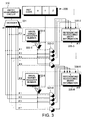
- the instruction-issuing circuit 300 used in the issue stage comprises an entry management circuit 310, a reference relation setting circuit 320, an instruction out-of-order buffer 330, and a ready flag setting circuit 340.
- An instruction stored in the D-stage storing circuit 200 (e.g. instruction latch) comprises an instruction code field 201, an X-operand field 202, a Y-operand field 203, and a Z-operand field 204.
- the instruction code field 201 contains an instruction code (including an instruction type). Normally, the X-operand field 202 contains the write register number, the Y-operand field 203 contains the first read register number, and the Z-operand field 204 contains the second read register number.
- the instruction out-of-order buffer 330 comprises a plurality of entries, each of which includes a validity flag 331, a write target register number field 332, a Y-operand ready flag 333, a Z-operand ready flag 334, a Y-operand referencing succeeding-entry information field 335, and a Z-operand referencing succeeding-entry information field 336.
- the validity flag 331 indicates whether the entry is "valid" or "invalid.”
- the write target register number field 332 contains the number of a register into which the instruction writes the result.
- the Y-operand ready flag 333 and the Z-operand ready flag 334 indicate whether or not the Y operand or the Z operand may be referenced (ready), respectively.
- the Y-operand ready flag 333 and the Z-operand ready flag 334 are updated by the ready flag setting circuit 340.
- the Y-operand referencing succeeding-entry information field 335 and the Z-operand referencing succeeding-entry information field 336 contain information about the position (that is, number) of an entry which contains a succeeding instruction which will reference the result of the instruction of this entry as the Y operand or the Z operand, respectively.
- the Y-operand referencing succeeding-entry information field 335 and the Z-operand referencing succeeding-entry information field 336 are each (number of entries of the instruction out-of-order buffer 330-1) bits in width. A bit in each of these fields corresponds to an entry, except this entry, of the instruction out-of-order buffer 330.
- the Y-operand referencing succeeding-entry information field 335 and the Z-operand referencing succeeding-entry information field 336 are set by the reference relation setting circuit 320.
- the entry management circuit 310 keeps track of the usage status of the entries of the instruction out-of-order buffer 330. That is, from the entries whose validity flag 331 is "invalid", the circuit selects an entry into which a new instruction is to be stored. To do so, the circuit, for example, selects from the "invalid" entries an entry with the smallest entry number.
- One example of such a circuit is a priority encoder.
- the validity flag 331 of the entry is set to "valid.”
- the validity flag 331 of the entry from which the instruction is issued is set to "invalid.”
- the reference relation setting circuit 320 comprises a decoder 321, and comparators 322 and logical product circuits 323 each provided for an entry of the instruction out-of-order buffer 330.
- the decoder 321 decodes an entry number output from the entry management circuit 310, indicating the entry into which a new instruction is to be stored.
- the instruction out-of-order buffer 330 is assumed to have eight entries, #1 to #8. Of course, the number of entries may be changed according to the system requirements. In this case, the decoder 321 has eight decode signal lines each corresponding to an entry.
- the instruction stored in the D-stage storing circuit 200 is stored in one of the entries of the instruction out-of-order buffer 330 according to the output from the decoder 321.
- the comparator 322 of each of the other entries compares the register number in the Y-operand field 203 and the register number in the Z-operand field 204 of the D-stage storing circuit 200 with the register number in the write target register number field 332 of that entry. If they match, the comparator 322 asserts its output.
- the logical product circuit 323 generates the logical product of the output from the comparator 322 and that from the decoder 321.
- each entry of the instruction out-of-order buffer 330 has the logical product circuit 323 for each of the other entries of the instruction out-of-order buffer 330.
- entry #3 of the instruction out-of-order buffer 330 has seven logical product circuits 323-3, that is, one for each of entries #1, #2, #4-#8.
- entry #8 has seven logical product circuits 323-8, that is, one for each of entries #1-#7.
- the output from the logical product circuit 323 is stored in the Y-operand referencing succeeding-entry information field 335 and the Z-operand referencing succeeding-entry information field 336.
- the reference relation setting circuit 320 sets the reference relation information in the Y-operand referencing succeeding-entry information field 335 and the Z-operand referencing succeeding-entry information field 336 of each of the preceding instructions.
- this reference relation information will be used later to quickly determine whether such a succeeding instruction may be issued.
- the ready flag setting circuit 340 comprises an issue instruction control circuit 341 and a selector 342.
- the issue instruction control circuit 341 searches the instruction out-of-order buffer 330 for an entry whose validity flag 331 is "valid" and whose Y-operand ready flag 333 and Z-operand ready flag 334 are "ready”. If such an entry is found, the circuit selects the instruction as an instruction that may be issued. The selected entry number is sent via a signal line 349 to the selector 342 for use as the control signal.
- the selector 342 outputs the Y-operand referencing succeeding-entry information field 335 and the Z-operand referencing succeeding-entry information field 336 contained in the entry specified by the issue instruction control circuit 341. It should be noted that, although the Y-operand referencing succeeding-entry information field 335 and the Z-operand referencing succeeding-entry information field 336 are each seven bits long, the selector 342 adds one extra bit for the entry itself and outputs eight bits. In this case, the added bit will never be asserted.
- the bits of the selected Y-operand referencing succeeding-entry information field 335 and the Z-operand referencing succeeding-entry information field 336 are set in the Y-operand ready flag 333 and the Z-operand ready flag 334, respectively.
- the first bit of the seven bits contained in the Y-operand referencing succeeding-entry information field 335-8 of entry #8 is set in the Y-operand ready flag 333-1
- the second bit is set in the Y-operand ready flag 333-2, and so on
- the seventh bit is set in the Y-operand ready flag 333-7.
- the logical low-level signal is sent to the Y-operand ready flag 333-8.
- the contents of the Z-operand referencing succeeding-entry information field 336 are set in the Z-operand ready flag 334.
- the Y operand ready flag or the Z operand ready flag of the succeeding instruction that references the write target register of the instruction that was issued may be set.
- the instruction string used for operation description is composed of two instructions: instruction 1 and instruction 2.
- Instruction 1 is an addition instruction that adds up the contents of register S2 and those of register S3 and stores the result into register S7.
- Instruction 2 is a subtraction instruction that subtracts the contents of register S10 from the contents of register S7 and stores the result into register S5. That is, the value generated by instruction 1 is stored in register S7 and is referenced as the Y operand of instruction 2. How this operation is executed will be described by referring to the instruction string shown in FIG. 5.
- instruction 1 is first read from the instruction buffer 100 into the D-stage storing circuit 200 at time T1.
- instruction 1 is decoded and is stored into the instruction out-of-order buffer 330 of the instruction-issuing circuit 300.
- instruction 1 is stored in entry #3 of the instruction out-of-order buffer 330 of the instruction-issuing circuit 300.
- instruction 2 is read from the instruction buffer 100 into the D-stage storing circuit 200.
- instruction 2 is decoded and is stored in the instruction out-of-order buffer 330.
- instruction 2 is stored in entry #8 of the instruction out-of-order buffer 330 of the instruction-issuing circuit 300.
- the decoder 321 assets only the signal line corresponding to #8. Therefore, the contents of the X-operand field 202 of the D-stage storing circuit 200 are stored in the write target register number field 332-8 of entry #8 of the instruction out-of-order buffer 330.
- the register number stored in the write target register number field 332-3 of entry #3 of the instruction out-of-order buffer 330 matches the register number stored in the Y-operand field 203 of the D-stage storing circuit 200.
- the issue instruction control circuit 341 detects that condition and sends the issue request to the selector 342.
- the selector 342 selects the Y-operand referencing succeeding-entry information field 335-3 and the Z-operand referencing succeeding-entry information field 336-3 of entry #3 and sets them in the Y-operand ready flag 333 and the Z-operand ready flag 334. Because only the bit corresponding to entry #8 of the Y-operand referencing succeeding-entry information field 335-3 is logically high, the Y-operand ready flag 333-8 corresponding to entry #8 is set.
- the operands of instruction 1 issued at time 8 are read. Also, at T9, the issue condition for instruction 2 is satisfied because Y-operand ready flag 333-8 of entry #8 was set at T8.
- the issue instruction control circuit 341 detects this condition and sends the an issue request for entry #8 to the selector 342.
- instruction 1 is executed by the operation unit 700, and the result is stored in the W-stage storing circuit 800. Also, at T10, the Z operand of instruction 2 is read from the register 500.
- the operation result of instruction 1 stored in the W-stage storing circuit 800 is written into the register 500.
- the operation result of instruction 1 stored in the W-stage storing circuit 800 is used as the first input to the operation unit 700, that is, as an input to the Y operand of instruction 2, through an operand bypass described above. This allows instruction 2 to be executed in the operation unit 700 at T11 with the result stored in the W-stage storing circuit 800.
- the operation result of instruction 2 stored in the W-stage storing circuit 800 is then written into the register 500.
- the Y-operand referencing succeeding-entry information field 335 and the Z-operand referencing succeeding-entry information field 336 are provided in the instruction out-of-order buffer 330, and the numbers of entries, each referencing the execution result of the instruction as the Y operand or the Z operand, are set in advance in those fields.
- the ready flag setting circuit 340 can immediately set the ready status of the Y operand and the Z operand into the Y-operand ready flag and the Z-operand ready flag 334.
- the instruction-issuing circuit sets, in advance, the information about a succeeding instruction which will reference the execution result of a preceding instruction. Therefore, when the preceding instruction is issued, it is possible to immediately determine whether the succeeding instruction may be issued.
Landscapes
- Engineering & Computer Science (AREA)
- Software Systems (AREA)
- Theoretical Computer Science (AREA)
- Physics & Mathematics (AREA)
- General Engineering & Computer Science (AREA)
- General Physics & Mathematics (AREA)
- Advance Control (AREA)
Applications Claiming Priority (2)
| Application Number | Priority Date | Filing Date | Title |
|---|---|---|---|
| JP33936698 | 1998-11-30 | ||
| JP10339366A JP2000163265A (ja) | 1998-11-30 | 1998-11-30 | 命令発行回路 |
Publications (2)
| Publication Number | Publication Date |
|---|---|
| EP1006439A1 true EP1006439A1 (de) | 2000-06-07 |
| EP1006439B1 EP1006439B1 (de) | 2005-10-26 |
Family
ID=18326797
Family Applications (1)
| Application Number | Title | Priority Date | Filing Date |
|---|---|---|---|
| EP99123697A Expired - Lifetime EP1006439B1 (de) | 1998-11-30 | 1999-11-29 | Instruktionaussendungs Schaltkreis und Verfahren für Ausführung ausserhalb der Reihenfolge, die Information zu Datenabhängigkeiten zu einer Instruktion speichern, wenn eine folgende Instruktion in einem Instruktionsbuffer gespeichert wird |
Country Status (4)
| Country | Link |
|---|---|
| US (1) | US6553484B1 (de) |
| EP (1) | EP1006439B1 (de) |
| JP (1) | JP2000163265A (de) |
| DE (1) | DE69927910T2 (de) |
Families Citing this family (7)
| Publication number | Priority date | Publication date | Assignee | Title |
|---|---|---|---|---|
| US6954848B2 (en) * | 2002-01-02 | 2005-10-11 | Intel Corporation | Marking in history table instructions slowable/delayable for subsequent executions when result is not used immediately |
| US6981166B2 (en) * | 2002-01-07 | 2005-12-27 | International Business Machines Corporation | Method, apparatus, and computer program product for pacing clocked operations |
| US20080168260A1 (en) * | 2007-01-08 | 2008-07-10 | Victor Zyuban | Symbolic Execution of Instructions on In-Order Processors |
| US9110656B2 (en) * | 2011-08-16 | 2015-08-18 | Freescale Semiconductor, Inc. | Systems and methods for handling instructions of in-order and out-of-order execution queues |
| US9971600B2 (en) * | 2015-06-26 | 2018-05-15 | International Business Machines Corporation | Techniques to wake-up dependent instructions for back-to-back issue in a microprocessor |
| JP7020304B2 (ja) * | 2018-06-07 | 2022-02-16 | 富士通株式会社 | 演算処理装置及び演算処理装置の制御方法 |
| CN114816526B (zh) * | 2022-04-19 | 2022-11-11 | 北京微核芯科技有限公司 | 基于操作数域复用的多操作数指令的处理方法及其装置 |
Citations (4)
| Publication number | Priority date | Publication date | Assignee | Title |
|---|---|---|---|---|
| WO1993020505A2 (en) * | 1992-03-31 | 1993-10-14 | Seiko Epson Corporation | Superscalar risc instruction scheduling |
| WO1994016384A1 (en) * | 1992-12-31 | 1994-07-21 | Seiko Epson Corporation | System and method for register renaming |
| US5812812A (en) * | 1996-11-04 | 1998-09-22 | International Business Machines Corporation | Method and system of implementing an early data dependency resolution mechanism in a high-performance data processing system utilizing out-of-order instruction issue |
| US5941983A (en) * | 1997-06-24 | 1999-08-24 | Hewlett-Packard Company | Out-of-order execution using encoded dependencies between instructions in queues to determine stall values that control issurance of instructions from the queues |
Family Cites Families (3)
| Publication number | Priority date | Publication date | Assignee | Title |
|---|---|---|---|---|
| US5471591A (en) * | 1990-06-29 | 1995-11-28 | Digital Equipment Corporation | Combined write-operand queue and read-after-write dependency scoreboard |
| US5761105A (en) * | 1995-09-26 | 1998-06-02 | Advanced Micro Devices, Inc. | Reservation station including addressable constant store for a floating point processing unit |
| JP2894438B2 (ja) | 1996-11-25 | 1999-05-24 | 日本電気株式会社 | パイプライン処理装置 |
-
1998
- 1998-11-30 JP JP10339366A patent/JP2000163265A/ja active Pending
-
1999
- 1999-11-29 DE DE69927910T patent/DE69927910T2/de not_active Expired - Fee Related
- 1999-11-29 EP EP99123697A patent/EP1006439B1/de not_active Expired - Lifetime
- 1999-11-30 US US09/450,769 patent/US6553484B1/en not_active Expired - Fee Related
Patent Citations (4)
| Publication number | Priority date | Publication date | Assignee | Title |
|---|---|---|---|---|
| WO1993020505A2 (en) * | 1992-03-31 | 1993-10-14 | Seiko Epson Corporation | Superscalar risc instruction scheduling |
| WO1994016384A1 (en) * | 1992-12-31 | 1994-07-21 | Seiko Epson Corporation | System and method for register renaming |
| US5812812A (en) * | 1996-11-04 | 1998-09-22 | International Business Machines Corporation | Method and system of implementing an early data dependency resolution mechanism in a high-performance data processing system utilizing out-of-order instruction issue |
| US5941983A (en) * | 1997-06-24 | 1999-08-24 | Hewlett-Packard Company | Out-of-order execution using encoded dependencies between instructions in queues to determine stall values that control issurance of instructions from the queues |
Also Published As
| Publication number | Publication date |
|---|---|
| DE69927910T2 (de) | 2006-07-20 |
| US6553484B1 (en) | 2003-04-22 |
| JP2000163265A (ja) | 2000-06-16 |
| DE69927910D1 (de) | 2005-12-01 |
| EP1006439B1 (de) | 2005-10-26 |
Similar Documents
| Publication | Publication Date | Title |
|---|---|---|
| US5961636A (en) | Checkpoint table for selective instruction flushing in a speculative execution unit | |
| US5611063A (en) | Method for executing speculative load instructions in high-performance processors | |
| US5887161A (en) | Issuing instructions in a processor supporting out-of-order execution | |
| US5809268A (en) | Method and system for tracking resource allocation within a processor | |
| US6237081B1 (en) | Queuing method and apparatus for facilitating the rejection of sequential instructions in a processor | |
| US20050278505A1 (en) | Microprocessor architecture including zero impact predictive data pre-fetch mechanism for pipeline data memory | |
| US5913048A (en) | Dispatching instructions in a processor supporting out-of-order execution | |
| US20040078559A1 (en) | Speculative execution control device for computer instructions and method for the same | |
| US20040064683A1 (en) | System and method for conditionally executing an instruction dependent on a previously existing condition | |
| US20030182536A1 (en) | Instruction issuing device and instruction issuing method | |
| US5740393A (en) | Instruction pointer limits in processor that performs speculative out-of-order instruction execution | |
| US20040064684A1 (en) | System and method for selectively updating pointers used in conditionally executed load/store with update instructions | |
| US5860014A (en) | Method and apparatus for improved recovery of processor state using history buffer | |
| US4541047A (en) | Pipelined data processing system | |
| US7454602B2 (en) | Pipeline having bifurcated global branch history buffer for indexing branch history table per instruction fetch group | |
| JP2003523574A (ja) | 2次リオーダ・バッファ・マイクロプロセッサ | |
| US5870612A (en) | Method and apparatus for condensed history buffer | |
| EP1006439B1 (de) | Instruktionaussendungs Schaltkreis und Verfahren für Ausführung ausserhalb der Reihenfolge, die Information zu Datenabhängigkeiten zu einer Instruktion speichern, wenn eine folgende Instruktion in einem Instruktionsbuffer gespeichert wird | |
| US7302553B2 (en) | Apparatus, system and method for quickly determining an oldest instruction in a non-moving instruction queue | |
| US6754813B1 (en) | Apparatus and method of processing information for suppression of branch prediction | |
| US7373486B2 (en) | Partially decoded register renamer | |
| US5944810A (en) | Superscalar processor for retiring multiple instructions in working register file by changing the status bits associated with each execution result to identify valid data | |
| US7765387B2 (en) | Program counter control method and processor thereof for controlling simultaneous execution of a plurality of instructions including branch instructions using a branch prediction mechanism and a delay instruction for branching | |
| US5878242A (en) | Method and system for forwarding instructions in a processor with increased forwarding probability | |
| US6016541A (en) | Instruction controlling system and method thereof |
Legal Events
| Date | Code | Title | Description |
|---|---|---|---|
| PUAI | Public reference made under article 153(3) epc to a published international application that has entered the european phase |
Free format text: ORIGINAL CODE: 0009012 |
|
| AK | Designated contracting states |
Kind code of ref document: A1 Designated state(s): CH DE FR LI |
|
| AX | Request for extension of the european patent |
Free format text: AL;LT;LV;MK;RO;SI |
|
| 17P | Request for examination filed |
Effective date: 20001207 |
|
| AKX | Designation fees paid |
Free format text: CH DE FR LI |
|
| 17Q | First examination report despatched |
Effective date: 20010122 |
|
| GRAP | Despatch of communication of intention to grant a patent |
Free format text: ORIGINAL CODE: EPIDOSNIGR1 |
|
| GRAS | Grant fee paid |
Free format text: ORIGINAL CODE: EPIDOSNIGR3 |
|
| GRAA | (expected) grant |
Free format text: ORIGINAL CODE: 0009210 |
|
| AK | Designated contracting states |
Kind code of ref document: B1 Designated state(s): CH DE FR LI |
|
| REG | Reference to a national code |
Ref country code: CH Ref legal event code: EP |
|
| REF | Corresponds to: |
Ref document number: 69927910 Country of ref document: DE Date of ref document: 20051201 Kind code of ref document: P |
|
| REG | Reference to a national code |
Ref country code: CH Ref legal event code: NV Representative=s name: E. BLUM & CO. PATENTANWAELTE |
|
| ET | Fr: translation filed | ||
| PLBE | No opposition filed within time limit |
Free format text: ORIGINAL CODE: 0009261 |
|
| STAA | Information on the status of an ep patent application or granted ep patent |
Free format text: STATUS: NO OPPOSITION FILED WITHIN TIME LIMIT |
|
| 26N | No opposition filed |
Effective date: 20060727 |
|
| REG | Reference to a national code |
Ref country code: CH Ref legal event code: PFA Owner name: NEC CORPORATION Free format text: NEC CORPORATION#7-1, SHIBA 5-CHOME, MINATO-KU#TOKYO (JP) -TRANSFER TO- NEC CORPORATION#7-1, SHIBA 5-CHOME, MINATO-KU#TOKYO (JP) |
|
| PGFP | Annual fee paid to national office [announced via postgrant information from national office to epo] |
Ref country code: DE Payment date: 20071122 Year of fee payment: 9 |
|
| PGFP | Annual fee paid to national office [announced via postgrant information from national office to epo] |
Ref country code: CH Payment date: 20071128 Year of fee payment: 9 |
|
| PGFP | Annual fee paid to national office [announced via postgrant information from national office to epo] |
Ref country code: FR Payment date: 20071108 Year of fee payment: 9 |
|
| REG | Reference to a national code |
Ref country code: CH Ref legal event code: PL |
|
| REG | Reference to a national code |
Ref country code: FR Ref legal event code: ST Effective date: 20090731 |
|
| PG25 | Lapsed in a contracting state [announced via postgrant information from national office to epo] |
Ref country code: LI Free format text: LAPSE BECAUSE OF NON-PAYMENT OF DUE FEES Effective date: 20081130 Ref country code: DE Free format text: LAPSE BECAUSE OF NON-PAYMENT OF DUE FEES Effective date: 20090603 Ref country code: CH Free format text: LAPSE BECAUSE OF NON-PAYMENT OF DUE FEES Effective date: 20081130 |
|
| PG25 | Lapsed in a contracting state [announced via postgrant information from national office to epo] |
Ref country code: FR Free format text: LAPSE BECAUSE OF NON-PAYMENT OF DUE FEES Effective date: 20081130 |