EP1006478A2 - Carte à puce, dispositif portable et procédé de mise à jour de données pour une carte à puce - Google Patents
Carte à puce, dispositif portable et procédé de mise à jour de données pour une carte à puce Download PDFInfo
- Publication number
- EP1006478A2 EP1006478A2 EP99118897A EP99118897A EP1006478A2 EP 1006478 A2 EP1006478 A2 EP 1006478A2 EP 99118897 A EP99118897 A EP 99118897A EP 99118897 A EP99118897 A EP 99118897A EP 1006478 A2 EP1006478 A2 EP 1006478A2
- Authority
- EP
- European Patent Office
- Prior art keywords
- data
- nonvolatile memory
- buffer region
- card
- commit buffer
- Prior art date
- Legal status (The legal status is an assumption and is not a legal conclusion. Google has not performed a legal analysis and makes no representation as to the accuracy of the status listed.)
- Granted
Links
Images




Classifications
-
- G—PHYSICS
- G07—CHECKING-DEVICES
- G07F—COIN-FREED OR LIKE APPARATUS
- G07F7/00—Mechanisms actuated by objects other than coins to free or to actuate vending, hiring, coin or paper currency dispensing or refunding apparatus
- G07F7/08—Mechanisms actuated by objects other than coins to free or to actuate vending, hiring, coin or paper currency dispensing or refunding apparatus by coded identity card or credit card or other personal identification means
- G07F7/10—Mechanisms actuated by objects other than coins to free or to actuate vending, hiring, coin or paper currency dispensing or refunding apparatus by coded identity card or credit card or other personal identification means together with a coded signal, e.g. in the form of personal identification information, like personal identification number [PIN] or biometric data
- G07F7/1008—Active credit-cards provided with means to personalise their use, e.g. with PIN-introduction/comparison system
-
- G—PHYSICS
- G06—COMPUTING OR CALCULATING; COUNTING
- G06Q—INFORMATION AND COMMUNICATION TECHNOLOGY [ICT] SPECIALLY ADAPTED FOR ADMINISTRATIVE, COMMERCIAL, FINANCIAL, MANAGERIAL OR SUPERVISORY PURPOSES; SYSTEMS OR METHODS SPECIALLY ADAPTED FOR ADMINISTRATIVE, COMMERCIAL, FINANCIAL, MANAGERIAL OR SUPERVISORY PURPOSES, NOT OTHERWISE PROVIDED FOR
- G06Q20/00—Payment architectures, schemes or protocols
- G06Q20/30—Payment architectures, schemes or protocols characterised by the use of specific devices or networks
- G06Q20/34—Payment architectures, schemes or protocols characterised by the use of specific devices or networks using cards, e.g. integrated circuit [IC] cards or magnetic cards
- G06Q20/341—Active cards, i.e. cards including their own processing means, e.g. including an IC or chip
-
- G—PHYSICS
- G06—COMPUTING OR CALCULATING; COUNTING
- G06Q—INFORMATION AND COMMUNICATION TECHNOLOGY [ICT] SPECIALLY ADAPTED FOR ADMINISTRATIVE, COMMERCIAL, FINANCIAL, MANAGERIAL OR SUPERVISORY PURPOSES; SYSTEMS OR METHODS SPECIALLY ADAPTED FOR ADMINISTRATIVE, COMMERCIAL, FINANCIAL, MANAGERIAL OR SUPERVISORY PURPOSES, NOT OTHERWISE PROVIDED FOR
- G06Q20/00—Payment architectures, schemes or protocols
- G06Q20/30—Payment architectures, schemes or protocols characterised by the use of specific devices or networks
- G06Q20/34—Payment architectures, schemes or protocols characterised by the use of specific devices or networks using cards, e.g. integrated circuit [IC] cards or magnetic cards
- G06Q20/355—Personalisation of cards for use
- G06Q20/3552—Downloading or loading of personalisation data
-
- G—PHYSICS
- G06—COMPUTING OR CALCULATING; COUNTING
- G06Q—INFORMATION AND COMMUNICATION TECHNOLOGY [ICT] SPECIALLY ADAPTED FOR ADMINISTRATIVE, COMMERCIAL, FINANCIAL, MANAGERIAL OR SUPERVISORY PURPOSES; SYSTEMS OR METHODS SPECIALLY ADAPTED FOR ADMINISTRATIVE, COMMERCIAL, FINANCIAL, MANAGERIAL OR SUPERVISORY PURPOSES, NOT OTHERWISE PROVIDED FOR
- G06Q20/00—Payment architectures, schemes or protocols
- G06Q20/30—Payment architectures, schemes or protocols characterised by the use of specific devices or networks
- G06Q20/34—Payment architectures, schemes or protocols characterised by the use of specific devices or networks using cards, e.g. integrated circuit [IC] cards or magnetic cards
- G06Q20/357—Cards having a plurality of specified features
- G06Q20/3576—Multiple memory zones on card
Definitions
- the present invention relates to an IC card which incorporates an environment for executing a program on a network, such as the Internet, and which has a function of loading an application.
- the present invention also relates to a portable device made of such an IC card or a similar card. Further, the present invention relates to a data updating method for an IC card.
- the data in an IC card is read or written under the control of a COS (Card Operating System). Since the data structure of the COS is known, the atomicity of the data updating utilizes the data structure and is therefore peculiar to the COS.
- COS Card Operating System
- the application enable direct reading or writing of data and that the atomicity of the data updating be ensured.
- the IC card is required to have a block transaction function. Since the data structure of the application is not known to the COS, the atomicity of the data updating under the control of the application should not be dependent on the data structure; it should be of a general-purpose nature.
- the IC card incorporating the execution environment is required to have a block transaction function.
- the atomicity of data updating in units of 1 byte, 2 bytes, 4 bytes and n bytes is demanded.
- the notion "commit buffer” is proposed.
- the commit buffer is realized in part of a persistent memory, such as an EEPROM.
- the EEPROM which is a nonvolatile memory, is restricted in terms of the number of times data can be written therein, and the time required for data writing is long.
- the object of the present invention is to provide an IC card, a portable device and a data updating method for an IC card, which enable a reduction in the number of times data is written in a nonvolatile memory and which also enable general-nature atomicity management.
- the present invention provides an IC card including a volatile memory and a nonvolatile memory and having a function of loading an application in the nonvolatile memory, the IC card comprising:
- the present invention also provides a portable device including a volatile memory and a nonvolatile memory and having a function of loading an application in the nonvolatile memory, the portable device comprising:
- the present further provides a data updating method for an IC card which includes a volatile memory and a nonvolatile memory and has a function of loading an application in the nonvolatile memory, the data updating method comprising the steps of:
- FIG. 1 shows a schematic structure of an IC card system.
- the IC card system comprises a terminal device 11 and an IC card 12.
- the terminal device 11 is made up of an operation unit 111 for executing an operation and receiving inputs entered by an operator, and a reader/writer 112 for reading data from the IC card 12 and writing data therein.
- the operation unit 111 and the reader/writer 112 are connected together by a line 113.
- the operation unit 111 is provided with a processor for executing an operation. It is also provided with input means which includes a human-system interface and from which external signals are entered. The input means processes a request made to the IC card 12, and also processes a result status.
- the reader/writer 112 receives a request sent from the operation unit 111, and sends that request to the IC card 12 inserted in a card insertion slot 120. Likewise, the reader/writer 112 receives a status signal from the IC card 12 and informs the operation unit 111 of the status of the IC card 12.
- the IC card 12 comprises: a contact 20 which is to be connected to an external apparatus when the IC card 12 serves as a portable device; a processor 21 for executing an operation and control; a volatile memory (RAM) 22 for temporarily storing data; a nonvolatile memory (EEPROM) 23 for permanently storing data; a coprocessor 24 serving as an auxiliary processor; and a ROM 5 for storing a virtual machine for interpreting a card domain, based on which a card operating system (COS) and an application are loaded or installed, and for further interpreting a byte code of the application.
- the IC card 12 performs communication with the reader/writer 112 by way of the contact 20.
- the nonvolatile memory 23 may be made of a flash memory, an FRAM, or the like.
- the processor 21 comprises a card applette CAP used for converting the application loaded from the terminal device 11 into data that can be used by the IC card 12.
- the coprocessor 24 described above is used when an operation that imposes a heavy load is executed.
- the coprocessor 24 executes the operation on the basis of instructions from the processor 21.
- Input data to the IC card 12 is entered by way of the contact 20 shown in FIG. 1, and normally it is stored in the RAM 22.
- the data, thus received, is analyzed and processed by the processor 21. If the data must be stored, it is written in the EEPROM 23 on the basis of instructions from the processor 21. If a special kind of operation is required, instructions for executing that operation are sent to the coprocessor 24.
- part of the EEPROM 23 can be used for temporarily storing the excessive data.
- the EEPROM 23 comprises: a system area 31 for storing a card ID, etc.; a BCC area 32 for area checking; a CB area 33 serving as a commit buffer area; a card data area 34 in which a slot management table 34a used for the management of slots and a shared table 34b indicating execution-permitted states among the application are stored; and a user application area 35 made up of a plurality of slots in each of which an application can be recorded.
- the BCC area 32 is used for determining whether correct data have been recorded in the card data area 34 and the user application area 35.
- the user application area 35 is made up of eight slots #0 to #7, and a user application is recorded in each of these slots.
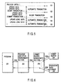
- the atomicity management function will be described in relation to a block transaction, referring to the program shown in FIG. 5.
- the COS automatically starts a transaction after " C-APDU" is received from the terminal device 11.
- the transaction is automatically brought to an end before "R-APDU" is sent to the terminal device 11.
- the terminal device is constantly in the chain transaction state.
- the synchronization points at which transactions are synchronized are as follows:
- FIG. 6 illustrates data reading procedures and data writing procedures.
- the processor 21 reads out a program 201 from a ROM 25, and the readout program 201 is executed by a program execution environment section 202.
- a commit buffer 204 is controlled by a commit buffer management section 203, and the readout program 201 is written or read from a persistent data storage 205.
- the commit buffer 204 is provided not only in the EEPROM 23 but also in the RAM 22.
- the persistent data storage 205 is provided in the user application area 35 of the EEPROM 23.
- the program execution environment section 202 requests that the commit buffer management section 203 execute data reading.
- the program execution environment section 202 designates the address and data length of the data to be read out, and informs the commit buffer management section 203 of the designated address and data length so that the commit buffer management section 203 can execute data reading.
- the commit buffer management section 203 first reads data from the commit buffer 204, and then read data from the persistent data storage 205. Values, thus read out, are supplied to the program execution environment section 202. The program execution environment section 202 sends the readout values to the program 201.
- the program execution environment section 202 requests that the commit buffer management section 203 execute data writing.
- the program execution environment section 202 designates the address, value and data length of the data to be written, and informs the commit buffer management section 203 of the designated address, value and data length so that the commit buffer management section 203 can execute data writing.
- the commit buffer management section 203 first writes data in the commit buffer 204, and then writes data in the persistent data storage 205.
- the program execution environment section 202 can know the number of bytes constituting the data that has to be read or written in response to the request made by the program 201. When the data is to be updated, the program execution environment section 202 informs the commit buffer management section 203 of the number of data items to be updated. The commit buffer management section 203 executes synchronization point processing if the commit buffer 204 is about to overflow.
- a request for writing n-byte data is made (ST1).
- a check is made to see whether or not the n-byte data can be written in the commit buffer 204 (ST2). If the n-byte data cannot be written in the commit buffer 204, a check is made to see whether or not a block transaction is being executed. If the block transaction is not executed then, commit information is left in the RAM 22 (ST4), and the data in the persistent storage 205 is made to reflect the data stored in the commit buffer 204 (ST5).
- the data in the commit buffer 204 is written in a free area of the persistent storage 204, or the data already recorded in the persistent storage 204 is overwritten with the data in the commit buffer 204.
- the n-byte data is written in the commit buffer 404 (ST6).
- step ST2 If the check in step ST2 shows that the n-byte data can be written in the commit buffer 204, the flow advances to step ST6, so as to write the n-byte data in the commit buffer 204.
- step ST3 If, in step ST3, the block transaction is detected as being executed, abort information is left in the RAM 22 (ST7), and the processing is brought to an end.
- a check is made to see whether or not the abort information is present in the RAM 22 (ST11). If the abort information is not present, a check is executed to see whether or not the commit buffer 204 stores the data (AI) of the designated address (ST12). If the data (AI) of the designated address is not present, a value is read from the persistent data storage 205 (ST13).
- step ST11 If the check in step ST11 shows that the abort information is present in the RAM 22, the flow advances to step ST13, so as to read a value from the persistent data storage 205 (ST13).
- step ST12 shows that the data of the designated address is present in the commit buffer 204
- a value is read from the commit buffer 204 (ST14).
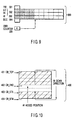
- the commit buffer 204 is made up of a commit buffer 300 provided in the RAM 22 of FIG. 9, and a commit buffer 400 provided in the EEPROM 23 of FIG. 10.
- the commit buffer 30 of the RAM 22 of FIG. 9 comprises a TID area 301, an address information area 302, an after-image area (to be abbreviated as an AI area) 303, and a BCC (byte check) area 304.
- the address information area 302 and the AI area 303 constitute one pair, and the commit buffer 300 provided in the RAM 22 is comprised of n pairs of them. The number of pairs registered is stored in the CBR counter 305 of the RAM 22.
- the commit buffer 400 provided in the EEPROM 23 shown in FIG. 10 is comprised m segments, each being similar in structure to the commit buffer 300 provided in the RAM 22.
- the start of the commit buffer 400 of the EEPROM 23 is a CB_TOP 401, and the terminating end of the commit buffer 400 is CB_BTM 404.
- CB_STA 403 indicates the position from which the present transaction uses the commit buffer 204 of the EEPROM 22, and CB_END 402 indicates the position from which the present transaction will use the commit buffer 204 of the EEPROM 22 next time.
- the commit buffer 400 is an area defined by the CB_STA 403 and the CB_END 402.
- Data is written in the commit buffer 300 of the RAM 22 in such a manner that the same data is written in the commit buffer 400 of the EEPROM 23.
- the commit buffer 300 of the RAM 22 is designed to correspond to the first page of the commit buffer 400 of the EEPROM 23.
- the commit buffer 400 is used by the present transaction in such a manner that the used area circulates from the CB_TOP 401 to the CB_MTM 404.
- the CB_STA 403 and CB_END 402 circulate from the CB-TOP 401 to the CB_BTM 404.
- the commit buffer management section 203 obtains data values by following the procedures (1)-(3) below.
- the commit buffer management section 203 writes data by following the procedures (1)-(3) below.
- the MSB of the TID area serves as a terminating buffer at which a transaction ends in the commit buffer.
- the commit buffer 400 of the EEPPROM 23 corresponds to m pages of the commit buffer 300 of the ROM 22 and is a circulation type. If the commit buffer 300 of the RAM 22 overflows, the data that cannot be stored therein is recorded on the page provided in the EEPROM 23 and indicated by the CB_END 402. Simultaneous with this, the data in the CB_END 402 is updated to indicate the next page.
- TID When the processing proceeds to a synchronization point, data is written on the page corresponding to the commit terminating flag of the TID. Subsequently, TID is incremented by "1". TID circulates in such a manner that its value is far larger than the number of pages provided in the commit buffer of the EEPROM 23.
- the commit buffer 400 of the EEPROM 23 is inspected when the IC card 12 is actuated next. More specifically, a page is searched for if the corresponding terminating flag of the TID 301 is set in the commit buffer 400 of the EEPROM 23. If the TID corresponding to the next page is not "TID+1", the commit buffer management section 203 determines that the EEPROM 23 includes a valid commit buffer whose data is not saved. Based on this determination, the actual EEPROM 205 is made to reflect the data stored in the EEPROM commit buffer 204 having the TID in question (roll forward). If no valid commit buffer exists, the actual EEPROM 205 is not subjected to the data reflection (roll back).
- the commit buffer management section 203 Before the transmission of "R-APDU", the commit buffer management section 203 writes a page that is likely to be regarded as invalid in the commit buffer 400 of the EEPROM 23. This prevents useless occurrence of roll forward.
- a structure for a commit buffer has been described, along with a processing method used for the commit buffer.
- the commit buffer and the processing method it is possible to reduce the number of times data is written in the EEPROM 23.
- the EEPOM commit buffer can be used in a uniform manner.
- the commit buffer shown in FIG. 6 is particularly advantageous when a CPU enabling a fast string search is adopted. That is, an address scan can be performed at high speed, and the data at a designated address can be easily searched.
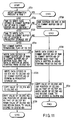
- the commit buffer management section 203 executes a check to see whether or not abort information is present in the RAM 22 (ST21). If the abort information is present, the processing is brought to an end. If no abort information is present, a check is made to see whether or not it is time to write the data stored in the commit buffer 300 of the RAM 22 in the commit buffer 400 of the EEPROM 23 (ST22). If it is, a check is made to see whether or not it is time to write the data stored in the commit buffer 400 of the EEPROM 23 in the persistent storage 205 (ST23). If it is, the commit buffer terminating flag of the TID 301 is set (ST24).
- the data in the commit buffer 300 of the RAM 22 is recorded in the commit buffer 400 of the EEPROM 23 in such a manner that the data is first written in the areas starting from CB_END 402 (ST25).
- the data stored in the CB_STA 403 to CB_END 402 of the commit buffer 400 of the EEPROM 23 is recorded in the persistent storage 205 (ST26).
- the value of the CB_STA 403 is copied to the CB_END 402 (ST27).
- the value of the CB_END 402 is shifted in this manner until it becomes equal to the value stored in the CB-BTM 404.
- the processing is brought to an end in a state where CB_END 402 correspond in position to CB_TOP 401 (ST28).
- step ST22 shows that it is not the time for data writing, an address 302 and an AI 303 are added to the commit buffer 300 of the RAM 22 (ST 29), and the processing is brought to an end.
- step ST23 shows that it is not the time for data writing
- the data in the commit buffer 300 of the RAM 22 is recorded in the commit buffer 400 of the EEPROM 23 in such a manner that the data is first written in the areas starting from CB_END 402 (ST30).
- the value of the CB_END 402 is shifted in this manner until it becomes equal to the value stored in the CB-BTM 404.
- the processing is brought to an end in a state where CB_END 402 correspond in position to CB_TOP 401 (ST31).
- step ST22 a check is made in step ST22 to see whether or not it is time to write the data stored in the commit buffer 300 of the RAM 22 in the commit buffer 400 of the EEPROM 23.
- the times when the data write operation referred to in step ST22 is started are a time at which the commit buffer 300 of the RAM 22 is considered to overflow when data write operation is executed next, and a time which is immediately before or after the start of a block transaction.
- the commit terminating flag of the TID 301 is searched for in the areas starting from CB_TOP 401 and ending to CB_BTM 404 (ST41). If the loop is taking place, the value of the CB_END 404 is used as the position of the present segment (ST42), and a check is made to see whether or not the commit terminating flag of the TID 301 is set in the commit buffer 400 of the EEPROM 23 (ST43). If the commit terminating flag is not set, the flow returns to step ST41.
- next TID is read from the commit buffer 400 of the EEPROM 23 and a check is made to see whether or not the TID has a value other than the expected value (i.e., "Present TID Value + 1") (ST44). If the TID has the expected value, the flow returns to step ST41; if it does not, the areas starting from CB_END 404 is inspected in the AI scan direction to search for a segment having the same TID (ST45).
- the oldest one is used as the CB-STA 403 (ST46).
- the persistent storage 205 is made to reflect the data stored in the commit buffer 400 of the EEPROM 23 (ST47).
- step ST41 the commit terminating flag is searched for and the loop is detected as having come to an end, the value of the CB_STA 403 is used as the position of the CB_END 402 (ST48).
- step ST47 or step ST48 After the end of either step ST47 or step ST48, the flow is brought to an end, and subsequently the processing for the CP-APDU reception is executed.
- the atomicity of data updating is ensured at all times even when the device is operating.
- the persistent data storage can withstand write operations executed a large number of times.
- the volume efficiency of the commit buffer of the persistent data storage can be enhanced per page, and the persistent data storage can withstand write operations performed a large number of times, and the number of times data must be written in the persistent data storage can be reduced.
- a number of commit buffer pages in the persistent register can be used to select a valid commit buffer, and data is prevented from being written concentratedly in a particular area of the persistent storage.
- the time required for reading data from the commit buffer can be as short as possible.
- the data read time can be remarkably short when no target data is found.
- the data read time can be also short to a certain extent when target data is found.
- the present invention is applicable not only to the IC card but also to a portable device having a similar structure.
Landscapes
- Engineering & Computer Science (AREA)
- Business, Economics & Management (AREA)
- Physics & Mathematics (AREA)
- General Physics & Mathematics (AREA)
- Microelectronics & Electronic Packaging (AREA)
- Computer Networks & Wireless Communication (AREA)
- Accounting & Taxation (AREA)
- Strategic Management (AREA)
- General Business, Economics & Management (AREA)
- Theoretical Computer Science (AREA)
- Information Retrieval, Db Structures And Fs Structures Therefor (AREA)
Applications Claiming Priority (2)
| Application Number | Priority Date | Filing Date | Title |
|---|---|---|---|
| JP34183898A JP3749798B2 (ja) | 1998-12-01 | 1998-12-01 | Icカードにおけるデータ書込方法およびicカードにおけるデータ読込方法 |
| JP34183898 | 1998-12-01 |
Publications (3)
| Publication Number | Publication Date |
|---|---|
| EP1006478A2 true EP1006478A2 (fr) | 2000-06-07 |
| EP1006478A3 EP1006478A3 (fr) | 2001-02-28 |
| EP1006478B1 EP1006478B1 (fr) | 2006-11-02 |
Family
ID=18349148
Family Applications (1)
| Application Number | Title | Priority Date | Filing Date |
|---|---|---|---|
| EP19990118897 Revoked EP1006478B1 (fr) | 1998-12-01 | 1999-09-24 | Carte à puce et procédé de mise à jour de données pour une carte à puce |
Country Status (3)
| Country | Link |
|---|---|
| EP (1) | EP1006478B1 (fr) |
| JP (1) | JP3749798B2 (fr) |
| DE (1) | DE69933841T8 (fr) |
Cited By (3)
| Publication number | Priority date | Publication date | Assignee | Title |
|---|---|---|---|---|
| SG168456A1 (en) * | 2009-07-15 | 2011-02-28 | Toshiba Kk | Portable electronic device, smartcard and control method for portable electronic device |
| US8819373B2 (en) | 2003-05-06 | 2014-08-26 | Giesecke & Devrient Gmbh | Managing persistent and temporary data objects in a portable data carrier |
| US9798739B2 (en) | 2012-09-20 | 2017-10-24 | Kabushiki Kaisha Toshiba | IC card and IC card control method |
Families Citing this family (2)
| Publication number | Priority date | Publication date | Assignee | Title |
|---|---|---|---|---|
| KR100951949B1 (ko) | 2007-11-15 | 2010-04-09 | 주식회사 케이티 | 스마트 카드에서의 데이터베이스 관리 시스템을 이용한정보 관리 방법 및 장치 |
| JP2009251818A (ja) * | 2008-04-03 | 2009-10-29 | Dainippon Printing Co Ltd | Icチップ用データ書き込み装置及びデータ書き込み方法 |
Family Cites Families (3)
| Publication number | Priority date | Publication date | Assignee | Title |
|---|---|---|---|---|
| FR2701578B1 (fr) * | 1993-02-16 | 1995-03-31 | Gemplus Card Int | Procédé d'écriture dans une mémoire non volatile, notamment dans une carte à mémoire. |
| BR9713267A (pt) * | 1996-10-25 | 2004-06-15 | Schlumberger Systems & Service | Cartão de circuito integrado para uso com um terminal, processo para uso com o mesmo, microcontrolador e processo para sua programação |
| US6488211B1 (en) * | 1997-05-15 | 2002-12-03 | Mondex International Limited | System and method for flexibly loading in IC card |
-
1998
- 1998-12-01 JP JP34183898A patent/JP3749798B2/ja not_active Expired - Lifetime
-
1999
- 1999-09-24 DE DE1999633841 patent/DE69933841T8/de active Active
- 1999-09-24 EP EP19990118897 patent/EP1006478B1/fr not_active Revoked
Cited By (4)
| Publication number | Priority date | Publication date | Assignee | Title |
|---|---|---|---|---|
| US8819373B2 (en) | 2003-05-06 | 2014-08-26 | Giesecke & Devrient Gmbh | Managing persistent and temporary data objects in a portable data carrier |
| SG168456A1 (en) * | 2009-07-15 | 2011-02-28 | Toshiba Kk | Portable electronic device, smartcard and control method for portable electronic device |
| US8645624B2 (en) | 2009-07-15 | 2014-02-04 | Kabushiki Kaisha Toshiba | Portable electronic device, smartcard and control method for portable electronic device |
| US9798739B2 (en) | 2012-09-20 | 2017-10-24 | Kabushiki Kaisha Toshiba | IC card and IC card control method |
Also Published As
| Publication number | Publication date |
|---|---|
| DE69933841T8 (de) | 2007-06-21 |
| EP1006478A3 (fr) | 2001-02-28 |
| DE69933841D1 (de) | 2006-12-14 |
| DE69933841T2 (de) | 2007-03-08 |
| EP1006478B1 (fr) | 2006-11-02 |
| JP3749798B2 (ja) | 2006-03-01 |
| JP2000172804A (ja) | 2000-06-23 |
Similar Documents
| Publication | Publication Date | Title |
|---|---|---|
| US5410700A (en) | Computer system which supports asynchronous commitment of data | |
| EP0964370B1 (fr) | Méthode et dispositif pour charger des codes d'instruction dans une mémoire et pour relier ces codes d'instruction | |
| US20040064635A1 (en) | Method of storing data in a non-volatile memory and apparatus therefor | |
| US5289588A (en) | Interlock acquisition for critical code section execution in a shared memory common-bus individually cached multiprocessor system | |
| US7406558B2 (en) | Software method of emulation of EEPROM memory | |
| KR100528973B1 (ko) | 가비지 콜렉션 방법 및 그 장치 | |
| EP1006478B1 (fr) | Carte à puce et procédé de mise à jour de données pour une carte à puce | |
| EP1510924B1 (fr) | Dispositif et méthode pour gérer des transactions avec écritures et lectures dans des mémoires EEPROM ou Flash | |
| US7168612B2 (en) | Method and apparatus for processing transactions in a data processing system | |
| CN110471626B (zh) | 应用于Java Card的Nor Flash管理层及方法 | |
| Oestreicher | Transactions in java card | |
| US7861114B2 (en) | System and method for recovery of memory transactions | |
| JPH11328293A (ja) | 媒体取引システム | |
| US20070130431A1 (en) | System, apparatus and method for reading data | |
| JP2001084180A (ja) | ファイル管理装置 | |
| US7243113B2 (en) | Information management system, information management method, and storage medium for managing execution records | |
| JPH0816881B2 (ja) | データベース更新方法 | |
| JP2001067210A (ja) | Icカードとicカードにおけるアプリケーションのインストール方法 | |
| JP2000148945A (ja) | Icカード | |
| JP2002342734A (ja) | 携帯可能電子装置およびその履歴データ記憶方法 | |
| JP7021465B2 (ja) | 電子情報記憶装置、icカード、データ復元方法、及びデータ復元プログラム | |
| JP4318494B2 (ja) | Icカード及びicカードプログラム | |
| JP4211890B2 (ja) | トランザクションにおけるメモリカードのデータの変更方法 | |
| US20080300019A1 (en) | Cellular phone | |
| JP2002504730A (ja) | コンピュータプログラムブロックのロード方法 |
Legal Events
| Date | Code | Title | Description |
|---|---|---|---|
| PUAI | Public reference made under article 153(3) epc to a published international application that has entered the european phase |
Free format text: ORIGINAL CODE: 0009012 |
|
| 17P | Request for examination filed |
Effective date: 19990924 |
|
| AK | Designated contracting states |
Kind code of ref document: A2 Designated state(s): DE FR GB |
|
| AX | Request for extension of the european patent |
Free format text: AL;LT;LV;MK;RO;SI |
|
| PUAL | Search report despatched |
Free format text: ORIGINAL CODE: 0009013 |
|
| AK | Designated contracting states |
Kind code of ref document: A3 Designated state(s): AT BE CH CY DE DK ES FI FR GB GR IE IT LI LU MC NL PT SE |
|
| AX | Request for extension of the european patent |
Free format text: AL;LT;LV;MK;RO;SI |
|
| RIC1 | Information provided on ipc code assigned before grant |
Free format text: 7G 06K 19/07 A, 7G 07F 7/10 B, 7G 06F 12/14 B |
|
| AKX | Designation fees paid |
Free format text: DE FR GB |
|
| 17Q | First examination report despatched |
Effective date: 20050210 |
|
| GRAP | Despatch of communication of intention to grant a patent |
Free format text: ORIGINAL CODE: EPIDOSNIGR1 |
|
| RTI1 | Title (correction) |
Free format text: IC CARD AND DATA UPDATING METHOD FOR IC CARD |
|
| GRAS | Grant fee paid |
Free format text: ORIGINAL CODE: EPIDOSNIGR3 |
|
| GRAA | (expected) grant |
Free format text: ORIGINAL CODE: 0009210 |
|
| AK | Designated contracting states |
Kind code of ref document: B1 Designated state(s): DE FR GB |
|
| REG | Reference to a national code |
Ref country code: GB Ref legal event code: FG4D |
|
| REF | Corresponds to: |
Ref document number: 69933841 Country of ref document: DE Date of ref document: 20061214 Kind code of ref document: P |
|
| ET | Fr: translation filed | ||
| PLAX | Notice of opposition and request to file observation + time limit sent |
Free format text: ORIGINAL CODE: EPIDOSNOBS2 |
|
| PLBI | Opposition filed |
Free format text: ORIGINAL CODE: 0009260 |
|
| 26 | Opposition filed |
Opponent name: GIESECKE & DEVRIENT GMBH Effective date: 20070801 |
|
| PLAF | Information modified related to communication of a notice of opposition and request to file observations + time limit |
Free format text: ORIGINAL CODE: EPIDOSCOBS2 |
|
| PLAF | Information modified related to communication of a notice of opposition and request to file observations + time limit |
Free format text: ORIGINAL CODE: EPIDOSCOBS2 |
|
| PLBB | Reply of patent proprietor to notice(s) of opposition received |
Free format text: ORIGINAL CODE: EPIDOSNOBS3 |
|
| RDAF | Communication despatched that patent is revoked |
Free format text: ORIGINAL CODE: EPIDOSNREV1 |
|
| APBM | Appeal reference recorded |
Free format text: ORIGINAL CODE: EPIDOSNREFNO |
|
| APBP | Date of receipt of notice of appeal recorded |
Free format text: ORIGINAL CODE: EPIDOSNNOA2O |
|
| APAH | Appeal reference modified |
Free format text: ORIGINAL CODE: EPIDOSCREFNO |
|
| RAP2 | Party data changed (patent owner data changed or rights of a patent transferred) |
Owner name: KABUSHIKI KAISHA TOSHIBA |
|
| APBQ | Date of receipt of statement of grounds of appeal recorded |
Free format text: ORIGINAL CODE: EPIDOSNNOA3O |
|
| PGFP | Annual fee paid to national office [announced via postgrant information from national office to epo] |
Ref country code: GB Payment date: 20140924 Year of fee payment: 16 |
|
| REG | Reference to a national code |
Ref country code: FR Ref legal event code: PLFP Year of fee payment: 17 |
|
| REG | Reference to a national code |
Ref country code: DE Ref legal event code: R103 Ref document number: 69933841 Country of ref document: DE Ref country code: DE Ref legal event code: R064 Ref document number: 69933841 Country of ref document: DE |
|
| APBU | Appeal procedure closed |
Free format text: ORIGINAL CODE: EPIDOSNNOA9O |
|
| PGFP | Annual fee paid to national office [announced via postgrant information from national office to epo] |
Ref country code: DE Payment date: 20150916 Year of fee payment: 17 |
|
| PGFP | Annual fee paid to national office [announced via postgrant information from national office to epo] |
Ref country code: FR Payment date: 20150629 Year of fee payment: 17 |
|
| RDAG | Patent revoked |
Free format text: ORIGINAL CODE: 0009271 |
|
| STAA | Information on the status of an ep patent application or granted ep patent |
Free format text: STATUS: PATENT REVOKED |
|
| 27W | Patent revoked |
Effective date: 20150911 |
|
| GBPR | Gb: patent revoked under art. 102 of the ep convention designating the uk as contracting state |
Effective date: 20150911 |