EP1006543A1 - Beleuchtete Membrane für einen elektrischen Schalter - Google Patents
Beleuchtete Membrane für einen elektrischen Schalter Download PDFInfo
- Publication number
- EP1006543A1 EP1006543A1 EP98122875A EP98122875A EP1006543A1 EP 1006543 A1 EP1006543 A1 EP 1006543A1 EP 98122875 A EP98122875 A EP 98122875A EP 98122875 A EP98122875 A EP 98122875A EP 1006543 A1 EP1006543 A1 EP 1006543A1
- Authority
- EP
- European Patent Office
- Prior art keywords
- layer
- contact
- aperture
- spacer
- illumination
- Prior art date
- Legal status (The legal status is an assumption and is not a legal conclusion. Google has not performed a legal analysis and makes no representation as to the accuracy of the status listed.)
- Granted
Links
- 239000012528 membrane Substances 0.000 title description 25
- 125000006850 spacer group Chemical group 0.000 claims abstract description 52
- 238000005286 illumination Methods 0.000 claims abstract description 38
- 230000000994 depressogenic effect Effects 0.000 claims description 7
- 239000010410 layer Substances 0.000 description 102
- 239000000463 material Substances 0.000 description 8
- 239000002861 polymer material Substances 0.000 description 7
- 229920000728 polyester Polymers 0.000 description 6
- 239000000758 substrate Substances 0.000 description 4
- 239000000853 adhesive Substances 0.000 description 3
- 230000001070 adhesive effect Effects 0.000 description 3
- 239000004020 conductor Substances 0.000 description 3
- 239000003990 capacitor Substances 0.000 description 2
- OKTJSMMVPCPJKN-UHFFFAOYSA-N Carbon Chemical compound [C] OKTJSMMVPCPJKN-UHFFFAOYSA-N 0.000 description 1
- RYGMFSIKBFXOCR-UHFFFAOYSA-N Copper Chemical compound [Cu] RYGMFSIKBFXOCR-UHFFFAOYSA-N 0.000 description 1
- PWHULOQIROXLJO-UHFFFAOYSA-N Manganese Chemical compound [Mn] PWHULOQIROXLJO-UHFFFAOYSA-N 0.000 description 1
- 239000005083 Zinc sulfide Substances 0.000 description 1
- 239000003522 acrylic cement Substances 0.000 description 1
- 239000012790 adhesive layer Substances 0.000 description 1
- BOGASOWHESMEKT-UHFFFAOYSA-N barium;oxotin Chemical compound [Ba].[Sn]=O BOGASOWHESMEKT-UHFFFAOYSA-N 0.000 description 1
- 229910052799 carbon Inorganic materials 0.000 description 1
- 229920001940 conductive polymer Polymers 0.000 description 1
- 229910052802 copper Inorganic materials 0.000 description 1
- 239000010949 copper Substances 0.000 description 1
- 238000005401 electroluminescence Methods 0.000 description 1
- 229910003437 indium oxide Inorganic materials 0.000 description 1
- PJXISJQVUVHSOJ-UHFFFAOYSA-N indium(iii) oxide Chemical compound [O-2].[O-2].[O-2].[In+3].[In+3] PJXISJQVUVHSOJ-UHFFFAOYSA-N 0.000 description 1
- AMGQUBHHOARCQH-UHFFFAOYSA-N indium;oxotin Chemical compound [In].[Sn]=O AMGQUBHHOARCQH-UHFFFAOYSA-N 0.000 description 1
- 229910052748 manganese Inorganic materials 0.000 description 1
- 239000011572 manganese Substances 0.000 description 1
- 230000003252 repetitive effect Effects 0.000 description 1
- 229910052709 silver Inorganic materials 0.000 description 1
- 239000004332 silver Substances 0.000 description 1
- 238000004544 sputter deposition Methods 0.000 description 1
- 229910052984 zinc sulfide Inorganic materials 0.000 description 1
- DRDVZXDWVBGGMH-UHFFFAOYSA-N zinc;sulfide Chemical compound [S-2].[Zn+2] DRDVZXDWVBGGMH-UHFFFAOYSA-N 0.000 description 1
Images


Classifications
-
- H—ELECTRICITY
- H01—ELECTRIC ELEMENTS
- H01H—ELECTRIC SWITCHES; RELAYS; SELECTORS; EMERGENCY PROTECTIVE DEVICES
- H01H13/00—Switches having rectilinearly-movable operating part or parts adapted for pushing or pulling in one direction only, e.g. push-button switch
- H01H13/70—Switches having rectilinearly-movable operating part or parts adapted for pushing or pulling in one direction only, e.g. push-button switch having a plurality of operating members associated with different sets of contacts, e.g. keyboard
- H01H13/702—Switches having rectilinearly-movable operating part or parts adapted for pushing or pulling in one direction only, e.g. push-button switch having a plurality of operating members associated with different sets of contacts, e.g. keyboard with contacts carried by or formed from layers in a multilayer structure, e.g. membrane switches
-
- H—ELECTRICITY
- H01—ELECTRIC ELEMENTS
- H01H—ELECTRIC SWITCHES; RELAYS; SELECTORS; EMERGENCY PROTECTIVE DEVICES
- H01H2219/00—Legends
- H01H2219/002—Legends replaceable; adaptable
- H01H2219/018—Electroluminescent panel
-
- H—ELECTRICITY
- H01—ELECTRIC ELEMENTS
- H01H—ELECTRIC SWITCHES; RELAYS; SELECTORS; EMERGENCY PROTECTIVE DEVICES
- H01H2219/00—Legends
- H01H2219/002—Legends replaceable; adaptable
- H01H2219/018—Electroluminescent panel
- H01H2219/02—Electroluminescent panel programmable
Definitions
- This invention generally relates to the art of electrical switches and, particularly, to an illuminated membrane-type electrical switch such as an electroluminescent switch in a keypad.
- Membrane electrical switches are used in a wide variety of applications and often are called "touch" switches.
- a switch includes a pair of non-conductive polymer film substrates or membranes on which thin conductive contacts are printed or otherwise laminated. At least one of the membranes is flexible.
- a single flexible membrane is used in conjunction with a more rigid circuit board.
- a normally open membrane switch a spacer layer is used between the membranes, with an aperture aligned with the contacts. When the flexible membrane(s) is depressed in the area of the aperture in the spacer layer, it flexes such that its contact engages the contact of the other membrane or circuit board to close the switch.
- conductors or leads connected to the switch contacts for connecting the contacts to external circuits. The conductors or leads often are printed on the flexible substrates or membranes.
- Such normally open membrane switches are popular as low profile, inexpensive alternatives for more complex mechanical switches.
- an electroluminescent switch includes an electroluminescent layer which defines a lamp typically having spaced transparent electrodes sandwiching an electroluminescent layer therebetween. Often a dielectric layer also is sandwiched between the two electrode layers. Conductive leads extend from the electrodes. When an AC voltage is applied across the leads, the current induced between the electrodes causes the electroluminescent layer to emit light, a phenomenon known as electroluminescence.
- an electroluminescent lamp essentially is a light emitting capacitor having a dielectric layer between two conductive electrode layers, at least one of which is transparent, and the dielectric layer may be an electroluminescent layer, or there may be a separate dielectric layer.
- one of the problems with membrane electrical switches such as illuminated or electroluminescent switches, is that the contact membranes or layers and spacer layers in the laminated switch are so thin that shorting occurs between the switch contacts because of abusive use or simply because of normal wear over time and repetitive usage. Such shorting causes unintentional and, most likely, undesirable closing of the switch.
- the present invention is directed to solving this problem by intentionally placing a dome in the flexible contact membrane or layer and having that dome project into an aperture in a spacer layer to, thereby, increase the spacing or distance between the normally open contacts of the membrane switch.
- An object, therefore, of the invention is to provide a new and improved membrane switch, such as an illuminated switch, which is not prone to shorting during use.
- the switch includes a resilient actuation layer having at least a light transmissive portion.
- a flexible illumination layer is disposed below the actuation layer.
- a spacer layer is disposed below the illumination layer and includes an aperture in registry with the light transmissive portion of the actuation layer.
- a contact layer is disposed below the spacer layer and includes a dome portion having a convex side projecting into the aperture in the spacer layer, with a conductive contact on the concave side of the dome portion.
- a circuit sheet is disposed below the contact layer and includes a conductive contact in registry with the contact on the contact layer for engagement therewith when the dome portion of the contact layer is depressed by the actuation layer through the flexible illumination layer.
- the illumination layer comprises an electroluminescent layer.
- the dome portion comprises an embossed portion of the contact layer.
- a second spacer layer is interposed between the contact layer and the circuit sheet, with an aperture in the second spacer layer in registry with the conductive contacts.
- a third spacer layer is interposed between the actuation layer and the illumination layer, with an aperture in the third spacer layer in registry with the apertures in the first and second spacer layers.
- the resilient actuation layer may include a dome-shaped tactile actuator portion in registry with the dome portion of the contact layer.
- the illuminated electrical membrane switch of the invention has a wide variety of applications, and Figure 1 shows an electrical display device, generally designated 10, which is but only one application of the invention.
- the display device has a display window 12 which will show illuminated data in response to information calculated by pushing one or more of a plurality of depressable switch buttons 14.
- Each switch button is operatively associated with one of the switches of the invention.
- One of the switch buttons is removed in Figure 1 to expose a dual-switch arrangement 16.
- the array of switch buttons and membrane switches form a keypad 18 for display device 10. It must be understood that the illuminated membrane switch of the invention is not limited to the particular device 10 shown in Figure 1.
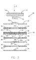
- the membrane switch includes a resilient actuation layer 22 above a spacer layer 24 which, in turn, is above an illumination layer 26, comprising several layers 42-52 which will be described subsequently.
- the illumination layer 26, in turn, is above a spacer layer 28 which, in turn, is above a contact membrane or layer 30 which, in turn, is above a spacer layer 32 which, in turn, is above a circuit sheet or board 34.
- All of layers 22-34 are laminated together by means of films of adhesive 36 applied to both sides of all three spacer layers 24, 28 and 32 so that the illuminated membrane switch 20 is laminated in the condition shown in Figure 2, below switch button 14.
- the adhesive may be an acrylic adhesive.
- Resilient actuation layer 22 is fabricated of a polymer material, such as a polyester, and includes a raised or embossed tactile dome 22a.
- the dome is immediately below or in registry with a depending actuating portion 14a of switch button 14.
- actuating portion 14a depresses dome 22a into engagement with illumination layer 26 and closes the switch, as described hereinafter, as dome 22a gives a tactile indication of switch actuation.
- Spacer layer 24 is fabricated of polymer material, such as a polyester material, and includes an aperture 24a.
- the aperture is immediately below or in the registry with tactile dome 22a of resilient actuation layer 22 so that the dome can be depressed through the aperture.
- Spacer layer 28 may be fabricated of polymer material, such as a polyester material, and includes an aperture 28a.
- the aperture is in registry with aperture 24a in spacer layer 24 and tactile dome 22a of actuation layer 22.
- the spacer layer 28 comprises only a layer of adhesive with an aperture 28a punched therethrough. The aperture 28a is punched before assembly when backing paper is adhered to both sides of the adhesive layer.
- Contact membrane or layer 30 is fabricated of polymer material, such as a polyester material, and includes a dome portion 30a.
- a switch contact 38 is printed or otherwise laminated to the underside of dome portion 30a.
- the dome portion has negligible tactility and is raised or embossed sufficiently to project into aperture 28a of spacer layer 28 as seen clearly in Figure 2. In fact, the dome portion can be raised to an extent that it touches the bottom of illumination layer 26, as shown.
- Spacer layer 32 is fabricated of polymer material, such as a polyester material, and includes an aperture 32a.
- the aperture is in registry with dome portion 32a of contact layer 30 and, particularly, contact 38.
- the spacer layers 24 and 32 may also be made in the preferred way of making the spacer layer 28.
- Circuit sheet or layer 34 is fabricated of polymer material and includes a switch contact 40 on the top side thereof.
- Contact 40 is in direct registry with switch contact 38 on the bottom of contact layer 30, so that contacts 38 and 40 can engage through aperture 32a in spacer layer 32.
- switch contacts 38 and 40 are connected to appropriate conductors or leads printed on or embedded in contact layer 30 and circuit sheet 34, the leads connecting the switch contacts to external circuits.
- contact 40 could be replaced with two contacts (not shown) comprising an open circuit. When contact 38 engages the two contacts on the circuit sheet, contact 38 would close the circuit path between the two contacts.
- switch button 14 In operation, when switch button 14 is depressed in the direction of arrow "A", actuator portion 14a of the switch button depresses and deforms tactile dome 22a of resilient actuation layer 22 and drives the dome through aperture 24a in spacer layer 24 and into engagement with illumination layer 26.
- the illumination layer is sufficiently flexible to drive dome portion 30a of contact layer 30 and switch contact 38 through aperture 32a in spacer layer 32 and into engagement with switch contact 40 of circuit sheet 34 to, thereby, close the illuminated electrical switch.
- Switch button 14 and at least tactile dome 22a of resilient actuation layer 22 are made of light transmissive material so that illumination layer 26 can be seen through aperture 24a in spacer layer 24 and through the actuation layer and the switch button.
- An ink layer 14b may be applied to the button 14 to selectively allow light from the illumination layer 26 to transmit only through selected areas of the top surface of the key.
- Illumination layer 26 may be an electroluminescent layer or lamp.
- illumination layer 26 includes a top transparent or translucent substrate 42 of polymer material, such as a polyester material.
- a top electrode film or layer 44 is deposited by printing or sputter coating onto the underside of substrate 42. Electrode layer 44 is transparent or translucent and can comprise such material as indium tin oxide or indium oxide.
- An illumination or electroluminescent layer 46 is printed onto the backside of top electrode 44.
- the illumination layer may be a zinc sulfide doped with copper and manganese.
- a dielectric layer 48 is disposed beneath illumination layer 46.
- the dielectric layer should be made of a material that has a high dielectric constant to raise the capacitance and has a reflective color to reflect light back toward illumination layer 46.
- the dielectric layer 48 is preferably made of barium tin oxide.
- a bottom electrode 50 such as of silver or carbon, is deposited against the bottom of dielectric layer 48, and an insulating layer 52 is printed or laminated over the rear electrode. From the foregoing, it can be seen that illumination layer 46 is sandwiched between a pair of electrodes 44 and 50 to define a light emitting capacitor as is known in the art. Of course, conductive leads (not shown) extend from the electrodes. This illumination layer 26 is sufficiently flexible to be moved into engagement with contact layer 30 to close switch 20.
Landscapes
- Push-Button Switches (AREA)
Priority Applications (2)
| Application Number | Priority Date | Filing Date | Title |
|---|---|---|---|
| DE69828885T DE69828885T2 (de) | 1998-12-02 | 1998-12-02 | "Elektrischer Sachlter mit beleuchteter Membran" |
| EP19980122875 EP1006543B1 (de) | 1998-12-02 | 1998-12-02 | Elektrischer Schalter mit beleuchteter Membran |
Applications Claiming Priority (1)
| Application Number | Priority Date | Filing Date | Title |
|---|---|---|---|
| EP19980122875 EP1006543B1 (de) | 1998-12-02 | 1998-12-02 | Elektrischer Schalter mit beleuchteter Membran |
Publications (2)
| Publication Number | Publication Date |
|---|---|
| EP1006543A1 true EP1006543A1 (de) | 2000-06-07 |
| EP1006543B1 EP1006543B1 (de) | 2005-02-02 |
Family
ID=8233076
Family Applications (1)
| Application Number | Title | Priority Date | Filing Date |
|---|---|---|---|
| EP19980122875 Expired - Lifetime EP1006543B1 (de) | 1998-12-02 | 1998-12-02 | Elektrischer Schalter mit beleuchteter Membran |
Country Status (2)
| Country | Link |
|---|---|
| EP (1) | EP1006543B1 (de) |
| DE (1) | DE69828885T2 (de) |
Cited By (3)
| Publication number | Priority date | Publication date | Assignee | Title |
|---|---|---|---|---|
| US6806815B1 (en) | 2000-05-02 | 2004-10-19 | Nokia Mobile Phones Ltd. | Keypad structure with inverted domes |
| US8432363B2 (en) | 2007-02-23 | 2013-04-30 | Nokia Corporation | Optical actuators in keypads |
| EP3243703A1 (de) * | 2016-05-12 | 2017-11-15 | DURA Automotive Holdings U.K., Ltd. | Äussere verkleidung für ein kraftfahrzeug |
Citations (6)
| Publication number | Priority date | Publication date | Assignee | Title |
|---|---|---|---|---|
| US4060703A (en) * | 1976-11-10 | 1977-11-29 | Everett Jr Seth Leroy | Keyboard switch assembly with tactile feedback having illuminated laminated layers including opaque or transparent conductive layer |
| EP0753985A2 (de) * | 1995-07-14 | 1997-01-15 | Matsushita Electric Industrial Co., Ltd. | Lumineszenzelement, Methode zur Herstellung desselben, und beleuchtetes Schaltelement damit |
| EP0763838A1 (de) * | 1995-08-07 | 1997-03-19 | Fuji Polymertech Co., Ltd | Beleuchteter Schalter |
| US5680160A (en) * | 1995-02-09 | 1997-10-21 | Leading Edge Industries, Inc. | Touch activated electroluminescent lamp and display switch |
| EP0847066A2 (de) * | 1996-12-05 | 1998-06-10 | Mitsubishi Denki Kabushiki Kaisha | Schalter mit Leuchtanzeige und sein Herstellungsverfahren |
| US5797482A (en) * | 1996-11-25 | 1998-08-25 | Metro-Mark, Inc. | Electroluminescent keypad |
-
1998
- 1998-12-02 EP EP19980122875 patent/EP1006543B1/de not_active Expired - Lifetime
- 1998-12-02 DE DE69828885T patent/DE69828885T2/de not_active Expired - Fee Related
Patent Citations (6)
| Publication number | Priority date | Publication date | Assignee | Title |
|---|---|---|---|---|
| US4060703A (en) * | 1976-11-10 | 1977-11-29 | Everett Jr Seth Leroy | Keyboard switch assembly with tactile feedback having illuminated laminated layers including opaque or transparent conductive layer |
| US5680160A (en) * | 1995-02-09 | 1997-10-21 | Leading Edge Industries, Inc. | Touch activated electroluminescent lamp and display switch |
| EP0753985A2 (de) * | 1995-07-14 | 1997-01-15 | Matsushita Electric Industrial Co., Ltd. | Lumineszenzelement, Methode zur Herstellung desselben, und beleuchtetes Schaltelement damit |
| EP0763838A1 (de) * | 1995-08-07 | 1997-03-19 | Fuji Polymertech Co., Ltd | Beleuchteter Schalter |
| US5797482A (en) * | 1996-11-25 | 1998-08-25 | Metro-Mark, Inc. | Electroluminescent keypad |
| EP0847066A2 (de) * | 1996-12-05 | 1998-06-10 | Mitsubishi Denki Kabushiki Kaisha | Schalter mit Leuchtanzeige und sein Herstellungsverfahren |
Cited By (4)
| Publication number | Priority date | Publication date | Assignee | Title |
|---|---|---|---|---|
| US6806815B1 (en) | 2000-05-02 | 2004-10-19 | Nokia Mobile Phones Ltd. | Keypad structure with inverted domes |
| US8432363B2 (en) | 2007-02-23 | 2013-04-30 | Nokia Corporation | Optical actuators in keypads |
| EP3243703A1 (de) * | 2016-05-12 | 2017-11-15 | DURA Automotive Holdings U.K., Ltd. | Äussere verkleidung für ein kraftfahrzeug |
| CN107399369A (zh) * | 2016-05-12 | 2017-11-28 | 杜拉汽车控股英国有限公司 | 用于机动车辆的外部装饰件 |
Also Published As
| Publication number | Publication date |
|---|---|
| DE69828885T2 (de) | 2006-01-19 |
| DE69828885D1 (de) | 2005-03-10 |
| EP1006543B1 (de) | 2005-02-02 |
Similar Documents
| Publication | Publication Date | Title |
|---|---|---|
| KR200319458Y1 (ko) | 조광식 스위치 | |
| US5797482A (en) | Electroluminescent keypad | |
| US5138119A (en) | Backlit tactile keyboard with improved tactile and electrical characteristics | |
| KR100469037B1 (ko) | El 시트 및 이를 사용한 스위치 | |
| CN101488064B (zh) | 触摸屏及利用了该触摸屏的可动接点体和开关 | |
| EP0503197A2 (de) | Hintergrundbeleuchtete Tastatur mit Druckpunktauslösung und mit verbesserten elektrischen und taktilen Eigenschaften | |
| US7605338B2 (en) | Movable contact unit and switch using the same | |
| US6670565B2 (en) | Illuminated button switch | |
| JPH0935571A (ja) | 照光式スイッチユニット | |
| CN101488409B (zh) | 可动触点体及使用该可动触点体的开关 | |
| US20040069607A1 (en) | Illuminated membrane switch | |
| US20040007968A1 (en) | Lighted switch sheet and lighted switch unit using the same | |
| JPH09245969A (ja) | 分散型エレクトロ・ルミネセンス素子およびそれを用いた照光式スイッチユニット | |
| JP2007523456A (ja) | スイッチ | |
| EP1006543B1 (de) | Elektrischer Schalter mit beleuchteter Membran | |
| TW563144B (en) | Lighting unit and lighting apparatus using the same unit | |
| JP4101586B2 (ja) | 照光スイッチ | |
| JPH1139984A (ja) | El照光式スイッチ | |
| KR100514759B1 (ko) | 초박형 발광 키패드 | |
| WO2000011689A1 (en) | Illuminated membrane switch | |
| JPH1139983A (ja) | El照光シート及びel照光式スイッチ | |
| JP2004213924A (ja) | 照光式押釦スイッチ用部材及び携帯電話の照光式押釦スイッチ用部材 | |
| JP2000100281A (ja) | El表示付メンブレンスイッチ | |
| KR20060116057A (ko) | 이엘 램프시트 및 그의 제조 방법 | |
| KR100900498B1 (ko) | 유연성 인쇄회로기판이 내장된 이동통신 단말기의 키패드조립체 |
Legal Events
| Date | Code | Title | Description |
|---|---|---|---|
| PUAI | Public reference made under article 153(3) epc to a published international application that has entered the european phase |
Free format text: ORIGINAL CODE: 0009012 |
|
| AK | Designated contracting states |
Kind code of ref document: A1 Designated state(s): DE FI FR GB IT SE |
|
| AX | Request for extension of the european patent |
Free format text: AL;LT;LV;MK;RO;SI |
|
| 17P | Request for examination filed |
Effective date: 20001130 |
|
| AKX | Designation fees paid |
Free format text: DE FI FR GB IT SE |
|
| 17Q | First examination report despatched |
Effective date: 20040128 |
|
| GRAP | Despatch of communication of intention to grant a patent |
Free format text: ORIGINAL CODE: EPIDOSNIGR1 |
|
| GRAS | Grant fee paid |
Free format text: ORIGINAL CODE: EPIDOSNIGR3 |
|
| GRAA | (expected) grant |
Free format text: ORIGINAL CODE: 0009210 |
|
| AK | Designated contracting states |
Kind code of ref document: B1 Designated state(s): DE FI FR GB IT SE |
|
| REG | Reference to a national code |
Ref country code: GB Ref legal event code: FG4D |
|
| REF | Corresponds to: |
Ref document number: 69828885 Country of ref document: DE Date of ref document: 20050310 Kind code of ref document: P |
|
| REG | Reference to a national code |
Ref country code: SE Ref legal event code: TRGR |
|
| PLBE | No opposition filed within time limit |
Free format text: ORIGINAL CODE: 0009261 |
|
| STAA | Information on the status of an ep patent application or granted ep patent |
Free format text: STATUS: NO OPPOSITION FILED WITHIN TIME LIMIT |
|
| 26N | No opposition filed |
Effective date: 20051103 |
|
| ET | Fr: translation filed | ||
| PGFP | Annual fee paid to national office [announced via postgrant information from national office to epo] |
Ref country code: FR Payment date: 20061220 Year of fee payment: 9 |
|
| PGFP | Annual fee paid to national office [announced via postgrant information from national office to epo] |
Ref country code: GB Payment date: 20061222 Year of fee payment: 9 |
|
| PGFP | Annual fee paid to national office [announced via postgrant information from national office to epo] |
Ref country code: SE Payment date: 20061227 Year of fee payment: 9 |
|
| PGFP | Annual fee paid to national office [announced via postgrant information from national office to epo] |
Ref country code: FI Payment date: 20061228 Year of fee payment: 9 |
|
| PGFP | Annual fee paid to national office [announced via postgrant information from national office to epo] |
Ref country code: IT Payment date: 20061231 Year of fee payment: 9 |
|
| PGFP | Annual fee paid to national office [announced via postgrant information from national office to epo] |
Ref country code: DE Payment date: 20070131 Year of fee payment: 9 |
|
| PG25 | Lapsed in a contracting state [announced via postgrant information from national office to epo] |
Ref country code: FI Free format text: LAPSE BECAUSE OF NON-PAYMENT OF DUE FEES Effective date: 20071202 |
|
| EUG | Se: european patent has lapsed | ||
| GBPC | Gb: european patent ceased through non-payment of renewal fee |
Effective date: 20071202 |
|
| PG25 | Lapsed in a contracting state [announced via postgrant information from national office to epo] |
Ref country code: SE Free format text: LAPSE BECAUSE OF NON-PAYMENT OF DUE FEES Effective date: 20071203 Ref country code: DE Free format text: LAPSE BECAUSE OF NON-PAYMENT OF DUE FEES Effective date: 20080701 |
|
| REG | Reference to a national code |
Ref country code: FR Ref legal event code: ST Effective date: 20081020 |
|
| PG25 | Lapsed in a contracting state [announced via postgrant information from national office to epo] |
Ref country code: GB Free format text: LAPSE BECAUSE OF NON-PAYMENT OF DUE FEES Effective date: 20071202 |
|
| PG25 | Lapsed in a contracting state [announced via postgrant information from national office to epo] |
Ref country code: FR Free format text: LAPSE BECAUSE OF NON-PAYMENT OF DUE FEES Effective date: 20071231 |
|
| PG25 | Lapsed in a contracting state [announced via postgrant information from national office to epo] |
Ref country code: IT Free format text: LAPSE BECAUSE OF NON-PAYMENT OF DUE FEES Effective date: 20071202 |