EP1006556B1 - Teilchenoptische Anordnung und Verfahren zur teilchenoptischen Erzeugung von Mikrostrukturen - Google Patents
Teilchenoptische Anordnung und Verfahren zur teilchenoptischen Erzeugung von Mikrostrukturen Download PDFInfo
- Publication number
- EP1006556B1 EP1006556B1 EP99122179A EP99122179A EP1006556B1 EP 1006556 B1 EP1006556 B1 EP 1006556B1 EP 99122179 A EP99122179 A EP 99122179A EP 99122179 A EP99122179 A EP 99122179A EP 1006556 B1 EP1006556 B1 EP 1006556B1
- Authority
- EP
- European Patent Office
- Prior art keywords
- mask
- plane
- particle
- energy filter
- optical
- Prior art date
- Legal status (The legal status is an assumption and is not a legal conclusion. Google has not performed a legal analysis and makes no representation as to the accuracy of the status listed.)
- Expired - Lifetime
Links
- 238000004519 manufacturing process Methods 0.000 title 1
- 239000002245 particle Substances 0.000 claims description 36
- 238000003384 imaging method Methods 0.000 claims description 14
- 230000033001 locomotion Effects 0.000 claims description 13
- 230000003287 optical effect Effects 0.000 claims description 10
- 238000012634 optical imaging Methods 0.000 claims description 7
- 238000000034 method Methods 0.000 claims description 6
- 239000000463 material Substances 0.000 claims description 4
- 238000011144 upstream manufacturing Methods 0.000 claims 1
- 235000012431 wafers Nutrition 0.000 description 12
- 239000012528 membrane Substances 0.000 description 8
- 230000005284 excitation Effects 0.000 description 3
- 238000010521 absorption reaction Methods 0.000 description 2
- 238000010586 diagram Methods 0.000 description 2
- 239000006185 dispersion Substances 0.000 description 2
- 230000003993 interaction Effects 0.000 description 2
- 238000001459 lithography Methods 0.000 description 2
- 239000004065 semiconductor Substances 0.000 description 2
- 238000000926 separation method Methods 0.000 description 2
- VYPSYNLAJGMNEJ-UHFFFAOYSA-N Silicium dioxide Chemical compound O=[Si]=O VYPSYNLAJGMNEJ-UHFFFAOYSA-N 0.000 description 1
- 230000004075 alteration Effects 0.000 description 1
- 230000005540 biological transmission Effects 0.000 description 1
- 230000008878 coupling Effects 0.000 description 1
- 238000010168 coupling process Methods 0.000 description 1
- 238000005859 coupling reaction Methods 0.000 description 1
- 230000001419 dependent effect Effects 0.000 description 1
- 238000001914 filtration Methods 0.000 description 1
- 238000010438 heat treatment Methods 0.000 description 1
- 238000007689 inspection Methods 0.000 description 1
- 150000002500 ions Chemical class 0.000 description 1
- 238000013507 mapping Methods 0.000 description 1
- 230000000873 masking effect Effects 0.000 description 1
- 229910052814 silicon oxide Inorganic materials 0.000 description 1
- 230000003595 spectral effect Effects 0.000 description 1
- 238000001228 spectrum Methods 0.000 description 1
Images


Classifications
-
- H—ELECTRICITY
- H01—ELECTRIC ELEMENTS
- H01J—ELECTRIC DISCHARGE TUBES OR DISCHARGE LAMPS
- H01J37/00—Discharge tubes with provision for introducing objects or material to be exposed to the discharge, e.g. for the purpose of examination or processing thereof
- H01J37/30—Electron-beam or ion-beam tubes for localised treatment of objects
- H01J37/317—Electron-beam or ion-beam tubes for localised treatment of objects for changing properties of the objects or for applying thin layers thereon, e.g. for ion implantation
- H01J37/3174—Particle-beam lithography, e.g. electron beam lithography
-
- B—PERFORMING OPERATIONS; TRANSPORTING
- B82—NANOTECHNOLOGY
- B82Y—SPECIFIC USES OR APPLICATIONS OF NANOSTRUCTURES; MEASUREMENT OR ANALYSIS OF NANOSTRUCTURES; MANUFACTURE OR TREATMENT OF NANOSTRUCTURES
- B82Y10/00—Nanotechnology for information processing, storage or transmission, e.g. quantum computing or single electron logic
-
- B—PERFORMING OPERATIONS; TRANSPORTING
- B82—NANOTECHNOLOGY
- B82Y—SPECIFIC USES OR APPLICATIONS OF NANOSTRUCTURES; MEASUREMENT OR ANALYSIS OF NANOSTRUCTURES; MANUFACTURE OR TREATMENT OF NANOSTRUCTURES
- B82Y40/00—Manufacture or treatment of nanostructures
-
- H—ELECTRICITY
- H01—ELECTRIC ELEMENTS
- H01J—ELECTRIC DISCHARGE TUBES OR DISCHARGE LAMPS
- H01J37/00—Discharge tubes with provision for introducing objects or material to be exposed to the discharge, e.g. for the purpose of examination or processing thereof
- H01J37/02—Details
- H01J37/04—Arrangements of electrodes and associated parts for generating or controlling the discharge, e.g. electron-optical arrangement or ion-optical arrangement
- H01J37/05—Electron or ion-optical arrangements for separating electrons or ions according to their energy or mass
Definitions
- the particle-optical arrangement according to the invention has a microstructure-bearing Mask downstream imaging energy filter on Using the energy filter will be Inelastically filtered particles of a given energy window filtered out.
- an imaging system downstream of the energy filter then takes the reduced size Illustration of the mask in the image or projection plane.
- the invention is therefore based on the idea for the generation of contrast Separation of the particles according to their energy or according to their energetic difference Use interaction with the mask to be imaged. Since the energy loss of Particles strongly element-specific, can be determined by using different Materials for the membrane on the one hand and the microstructure on the other hand, a high Create image contrast. It does not matter if both the membrane as also inelastically scatter the microstructure, as long as the energy loss spectra for the adequately distinguish the materials used in the membrane and the microstructure, so that an energetic separation of the inelastically scattered from the inelastically scattered Particles at the output of the energy filter is possible.
- the mask carrying the microstructure consists of one of the particles which spreads elastically Carrier film with an inelastically scattering microstructure.
- the inelastically scattered particles at the output of the energy filter filtered out, so that for imaging the mask only the elastically scattered particles contribute as they have the lowest spectral distribution.
- the image of the mask plane in the image plane should be such that the Image of the mask in the image plane is at most half as large as the mask (Magnification less than 0.5).
- the energy filter should preferably be designed as a so-called imaging energy filter be that a first input-side plane - the input image plane - achromatisch in one first output-side plane - output image plane - and a second input-side plane - Input diffraction plane - dispersive into a second output-side plane - dispersive Plane - maps.
- the mask should then be either in the first input-side plane arranged or through a mask downstream of the imaging stage in this first Input side level of the filter to be mapped.
- a specimen holder arranged, which serves to receive the wafer to be structured.
- This specimen holder should be in two mutually perpendicular directions perpendicular to the optical axis of the be particle-optical arrangement, be movable by motor.
- the mask level should also a mask receiving, in two mutually perpendicular directions, the again perpendicular to the optical axis of the particle-optical arrangement, be arranged motorically movable specimen holder.
- Movement-like coupling of the specimen holder in the mask plane with the movement of the specimen holder in the image plane can successively different areas of the Mask on different areas of the wafer to be arranged in the image plane imaged in an energy-filtered manner so that mask fields are formed by successive projection can be imaged that are larger than the transmitted image field.
- a condenser system may be provided between the particle source and the mask plane.
- Such a condenser system makes it possible to collimate in the mask plane Provide beam path.
- a first Deflection system between the particle source and the mask plane a first Deflection system, between the mask layer and the energy filter a second Deflection system and be provided behind the energy filter, a third deflection system.
- Each of these three deflection systems can in a known manner as Doppelablenksystem be educated.
- the first and the second deflection system are preferably such excited that a parallel to the optical axis entering the first deflection system Particle beam in the mask plane deflected to an off-axis area and behind the mask plane is directed back towards the optical axis.
- the third deflection system behind the energy filter is then again an off-axis Deflection.
- the particles used in conjunction with the invention for mask imaging can Be electrons or ions, wherein the use of electrons is preferred because of the Invention required components in principle of transmission electron microscopes are known.
- (1) is the crossover of a particle source, for example one Electron source, called.
- a condenser (2) forms this crossover plane (1) in real a crossover plane (3).
- the mask plane (4) is located - in the propagation direction of the particles - behind the crossover plane (3), so that one in the mask plane (4) arranged mask is illuminated over a large area and evenly.
- the mask plane (4) is arranged downstream of an energy filter (5) in the beam direction.
- This Energy filter is designed as a so-called imaging energy filter, the first input-side plane, the input image plane, achromatisch in a first output side Image plane, the output image plane, and a second input side plane, the Input diffraction plane, dispersive in a second output-side plane, the Selection level or dispersive plane maps.
- Such energy filters are for electrons for example, from US-A-4,740,704, US-A-4,760,261 or US-A-5,449,914. Their detailed structure therefore need not be discussed further here become.
- the mask plane (4) coincides with the Input image plane of the filter and the crossover plane (3) with the input diffraction plane the energy filter together.
- the energy filter (5) forms the mask plane (4) achromatically in the output image plane (6) and the crossover plane (3) achromatically in the Dispersion level (7) from; the magnification for both the image of the Input image plane as well as for the image of the input diffraction plane should be 1: 1, so that a largely symmetrical course of the particle trajectories in Energy filter is ensured, which in turn avoided aberrations in the filter become.
- a slit diaphragm is arranged through which particles, who have experienced a predetermined energy loss can be selected.
- the one by the Slit diaphragm (7) preset energy loss is on the element-specific Energy loss of the microstructure of the mask to be arranged in the mask plane (4) adjustable.
- Projection system (8, 9) In the propagation direction of the particles behind the slit diaphragm (7) follows Projection system (8, 9), through which the output image plane (6) of the energy filter (5) zoomed into the image plane (10) is mapped.
- the magnification of the Projection system is about 0.25, so that of the energy filter (5) transmitted Area of the mask plane (4) in the image plane (10) reduced to about a quarter appears.
- the figure 1 embodiment is no particle-optical selection of different areas in the mask plane (4) possible.
- For the corresponding movement of the mask and the wafer can be in the case of electron-optical Waferstages used in inspection equipment used here in the figure 1 but not shown.
- the movements of the Waferstages in the mask level (4) and in the image plane (10) are to be coupled together so that the ratio of the movement stroke of the mask and the movement stroke of the wafer Mapping scale between the mask layer (4) and the image plane (10) corresponds.
- the particle source is denoted by (11).
- a first condenser lens (12) produces a real image (11a) of the source (11) so-called crossover.
- the deflection system (13) is followed by a second condenser lens (14), which detects the Crossover (11a) maps to infinity.
- the mask plane (15) In the beam direction behind the second Condenser lens (14) in the parallel beam path is the mask plane (15).
- the Mask level is arranged for receiving the mask mask holder.
- the mask holder is in two mutually perpendicular Directions, both aligned perpendicular to the optical axis of the imaging system are, motorically movable to thereby different areas of the male To bring mask into the particle-optical imaging beam path.
- the mask plane is followed by a third condenser lens (16), through which the mask plane (15) is imaged in the input image plane (18) of the energy filter (19).
- the two Kondensorlinsen (14, 16) can also by a so-called condenser lens Einfeldlinse be realized.
- the energy filter (19) is an imaging energy filter that achromatically images the input image plane (18) into the output image plane (20) and simultaneously an input diffraction plane dispersive in an output side Selection level (21) maps.
- the selection plane (21) is again a slit diaphragm provided by which a predetermined energy loss is adjustable.
- Subsequent projection system (23, 24) is again a reduced figure of the image resulting in the output image plane (20) of the energy filter (19) Mask plane (15) in the final image plane (25).
- first deflection system (13) in the plane of the crossover (11a) in front of Masking plane (15) can be a distraction of the depending on the excitation of the deflection system Particle beam perpendicular to the optical axis, so that depending on the excitation of Deflection system (13) different lateral areas (15a, 15b, 15c) in the mask plane (15) are illuminated.
- the one in the mask plane (15) telecentric off-axis extending particle beam is through the third condenser lens (16) back in the direction deflected back optical axis.
- a second deflection system (17) in the rear Focal plane of the third condenser lens (16) is arranged, there is a return or Tilting of the particle beam, just that generated by the first deflection system (13) Deflection is directed so opposite, so that behind the second deflection system (17) the further propagation of the particle beam independent of that of the first deflection system generated deflection is. Consequently, the propagation of the particle beam is also within the energy filter (19) independent of that achieved at the mask level Beam deflection.
- a third deflection system (22) which deflects the beam around the optical beam Axis in the selection level (21) causes, again produces a final Beam deflection, which is coupled to the beam deflection in the mask plane such that adjacent areas in the mask level successively to each other lying areas in the image plane (25) are mapped.
- This particle-optical Beam deflection can total larger field areas in the mask plane (15) be successively filtered energy filtered in the image plane (25).
- the individual particle-optical Simplified components This is not the case with the deflection systems (13, 17, 22) imperative that they are arranged in each of the said crossover planes. Rather, it is important that the deflection systems at least virtual beam deflections to create the crossover planes. As far as the crossover planes for reasons of space for a simple beam deflection system are not accessible, the deflection systems in known manner, as the deflection system (22) behind the projection system (23, 24), also be designed as Doppelablenksysteme that only a virtual tilt in the cause crossover levels.
- the Condenser lenses and / or the projectile lenses pass through the particles off-axis may be refocusing of the respective lenses as well as a change in the the figures not shown stigmators and adjustment and correction elements in Depending on the distraction caused by the deflection systems may be required.
- the for this refocusing and / or the changes of the stigmators and adjusting and Correction elements required current and voltage changes are as a data table stored in the control computer, not shown, causing the Distractions are each associated with the associated current or voltage changes.
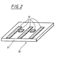
- FIG 2 is a schematic section through a in conjunction with the inventive arrangement usable mask shown.
- the mask (30) exists from a thin membrane (31), for example of silicon oxide, to which the desired Microstructures (32) are applied.
- the microstructures (32) have a different one Material as the membrane (31) so that the microstructures (32) interacting particles experience a different energy loss than those particles, which outside the microstructures (32) have transmitted the mask (30).
Landscapes
- Chemical & Material Sciences (AREA)
- Engineering & Computer Science (AREA)
- Nanotechnology (AREA)
- Analytical Chemistry (AREA)
- Physics & Mathematics (AREA)
- Crystallography & Structural Chemistry (AREA)
- Manufacturing & Machinery (AREA)
- General Physics & Mathematics (AREA)
- Condensed Matter Physics & Semiconductors (AREA)
- Mathematical Physics (AREA)
- Theoretical Computer Science (AREA)
- Electron Beam Exposure (AREA)
- Optical Elements Other Than Lenses (AREA)
- Exposure And Positioning Against Photoresist Photosensitive Materials (AREA)
Description
- Figur 1
- eine vereinfachte Prinzipskizze einer erfindungsgemäßen teilchenoptischen Anordnung;
- Figur 2
- eine perspektivische Darstellung eines Ausschnitts aus einer in Verbindung mit der Erfindung eingestzten Maske; und
- Figur 3
- die Prinzipskizze eines Ausführungsbeispiels der Erfindung mit teilchenoptischer Bereichsauswahl in der Maskenebene.
Claims (13)
- Teilchenoptische Anordnung mit einem zur Aufnahme einer Maske dienenden Maskenhalter in einer Maskenebene (4; 15) und einem dem Maskenhalter nachfolgenden abbildenden Energiefilter (5; 19), wobei die Maskenebene über das Energiefilter verkleinert in eine Bildebene (10; 25) abgebildet ist.
- Teilchenoptische Anordnung nach Anspruch 1, wobei das abbildende Energiefilter (5; 19) eine erste eingangsseitige Ebene (4; 18) achromatisch in eine erste ausgangsseitige Ebene (6; 20) und eine zweite eingangsseitige Ebene (3; 17) dispersiv in eine zweite ausgangsseitige Ebene (7; 21) abbildet und wobei die Maskenebene in der ersten eingangsseitigen Ebene (4; 18) angeordnet oder in diese abgebildet ist.
- Teilchenoptische Anordnung nach Anspruch 1 oder 2, wobei dem Energiefilter ein verkleinerndes Abbildungssystem (8, 9; 23, 24) nachgeordnet ist.
- Teilchenoptisches Abbildungssystem nach einem der Ansprüche 1-3, wobei in der Bildebene (10; 25) ein Präparathalter angeordnet ist, der in zwei zueinander senkrechten Richtungen motorisch bewegbar ist.
- Teilchenoptische Anordnung nach Anspruch 4, wobei der Maskenhalter in der Maskenebene (4; 15) in zwei zueinander senkrechten Richtungen motorisch bewegbar ist und die Bewegung des Maskenhalters und die Bewegung des Präparathalters miteinander gekoppelt sind.
- Teilchenoptisches Abbildungssystem nach einem der Ansprüche 1-5, wobei zwischen der Teilchenquelle (11) und der Maskenebene (4; 15) ein Kondensorsystem (2; 12, 14) vorgesehen ist.
- Teilchenoptisches Abbildungssystem nach einem der Ansprüche 1-6, wobei zwischen der Teilchenquelle (11) und der Maskenebene (15) ein erstes Ablenksystem (13), zwischen der Maskenebene und dem Energiefilter (19) ein zweites Ablenksystem (17) und dem Energiefilter nachgeschaltet ein drittes Ablenksystem (22) vorgesehen ist.
- Teilchenoptisches Abbildungssystem nach Anspruch 7, wobei das erste und zweite Ablenksystem (13, 17) derart erregt sind, daß ein parallel zur optischen Achse verlaufender Teilchenstrahl in der Maskenebene (15) einen außerachsialen Bereich (15a, 15c) durchläuft, hinter der Maskenebene (15) wieder in Richtung auf die optische Achse zurückgelenkt und hinter dem Energiefilter durch das dritte Ablenksystem (22) wieder auf einen außerachsialen Bereich in der Bildebene (25) abgelenkt wird.
- Teilchenoptisches Abbildungssystem nach Anspruch 8, wobei bei einer Änderung der durch die Ablenksysteme (13, 17, 20) bewirkten Ablänkung eine Änderung der Erregung der Kondensorlinsen (14, 16) und/oder weiterer Elemente wie Stigmatoren und Justier- und Korrekturelemente erfolgt.
- Teilchenoptisches Abbildungssystem nach einem der Ansprüche 1-9, wobei die Maskenebene (15) sich in einem kollimierten Strahlengang befindet.
- Verfahren zur teilchenoptischen Erzeugung von Mikrostrukturen, wobei eine Maske (30) mit inelastisch streuenden Mikrostrukturen (32) eingesetzt und über ein Energiefilter (5; 19) verkleinert auf einen Wafer abgebildet wird und wobei mit dem Energiefilter (5; 19) Teilchen mit einem voreingestellten Energieverlust selektiert werden.
- Verfahren nach Anspruch 11, wobei die Maske aus einer dünnen Trägerfolie (31) mit inelastisch streuenden Mikrostrukturen (32) besteht.
- Verfahren nach Anspruch 11 oder 12, wobei die Trägerfolie (31) aus einem elastisch streuenden Material besteht.
Applications Claiming Priority (2)
| Application Number | Priority Date | Filing Date | Title |
|---|---|---|---|
| DE19855629 | 1998-02-12 | ||
| DE19855629A DE19855629A1 (de) | 1998-12-02 | 1998-12-02 | Teilchenoptische Anordnung und Verfahren zur teilchenoptischen Erzeugung von Mikrostrukturen |
Publications (2)
| Publication Number | Publication Date |
|---|---|
| EP1006556A1 EP1006556A1 (de) | 2000-06-07 |
| EP1006556B1 true EP1006556B1 (de) | 2005-08-03 |
Family
ID=7889757
Family Applications (1)
| Application Number | Title | Priority Date | Filing Date |
|---|---|---|---|
| EP99122179A Expired - Lifetime EP1006556B1 (de) | 1998-12-02 | 1999-11-06 | Teilchenoptische Anordnung und Verfahren zur teilchenoptischen Erzeugung von Mikrostrukturen |
Country Status (6)
| Country | Link |
|---|---|
| US (1) | US6437353B1 (de) |
| EP (1) | EP1006556B1 (de) |
| JP (1) | JP2000173919A (de) |
| DE (2) | DE19855629A1 (de) |
| SG (1) | SG76640A1 (de) |
| TW (1) | TW454220B (de) |
Families Citing this family (10)
| Publication number | Priority date | Publication date | Assignee | Title |
|---|---|---|---|---|
| DE10034412A1 (de) * | 2000-07-14 | 2002-01-24 | Leo Elektronenmikroskopie Gmbh | Verfahren zur Elektronenstrahl-Lithographie und elektronen-optisches Lithographiesystem |
| DE10053488A1 (de) * | 2000-10-27 | 2002-05-08 | Volkswagen Ag | Anlage und Verfahren zur Aufbereitung von Shredder-Rückständen und Verwendung einer erzeugten Granulat-Fraktion |
| DE10053487A1 (de) * | 2000-10-27 | 2002-05-08 | Volkswagen Ag | Anlage und Verfahren zur Aufbereitung von Shredder-Rückständen |
| DE10053491A1 (de) * | 2000-10-27 | 2002-05-08 | Volkswagen Ag | Anlage und Verfahren zur Aufbereitung von Shredder-Rückständen und Verfahren einer erzeugten Flusen-Fraktion |
| DE10109965A1 (de) | 2001-03-01 | 2002-09-12 | Zeiss Carl | Teilchenoptische Linsenanordnung und Verfahren unter Einsatz einer solchen Linsenanordnung |
| DE10117025A1 (de) | 2001-04-05 | 2002-10-10 | Zeiss Carl | Teilchenoptische Vorrichtung,Beleuchtungsvorrichtung und Projektionssystem sowie Verfahren unter Verwendung derselben |
| DE102004037781A1 (de) | 2004-08-03 | 2006-02-23 | Carl Zeiss Nts Gmbh | Elektronenstrahlgerät |
| US7504648B2 (en) * | 2007-04-27 | 2009-03-17 | Carestream Health, Inc. | Method and apparatus for determining focus of a scanning system |
| DE102012007868A1 (de) * | 2012-04-19 | 2013-10-24 | Carl Zeiss Microscopy Gmbh | Transmissionselektronenmikroskopiesystem |
| CN103777364B (zh) * | 2013-12-13 | 2017-10-13 | 北京维信诺科技有限公司 | 一种分划板的制造方法 |
Family Cites Families (6)
| Publication number | Priority date | Publication date | Assignee | Title |
|---|---|---|---|---|
| DE3532699A1 (de) | 1985-09-13 | 1987-03-26 | Zeiss Carl Fa | Elektronenenergiefilter vom omega-typ |
| DE3532698A1 (de) | 1985-09-13 | 1987-03-26 | Zeiss Carl Fa | Elektronenenergiefilter vom alpha-typ |
| US5079112A (en) * | 1989-08-07 | 1992-01-07 | At&T Bell Laboratories | Device manufacture involving lithographic processing |
| DE4310559A1 (de) | 1993-03-26 | 1994-09-29 | Zeiss Carl Fa | Abbildendes Elektronenenergiefilter |
| EP0772225B1 (de) * | 1994-07-15 | 2003-03-19 | Hitachi, Ltd. | Elektronischer energiefilter |
| US5912469A (en) * | 1996-07-11 | 1999-06-15 | Nikon Corporation | Charged-particle-beam microlithography apparatus |
-
1998
- 1998-12-02 DE DE19855629A patent/DE19855629A1/de not_active Withdrawn
-
1999
- 1999-11-06 EP EP99122179A patent/EP1006556B1/de not_active Expired - Lifetime
- 1999-11-06 DE DE59912355T patent/DE59912355D1/de not_active Expired - Fee Related
- 1999-11-29 TW TW088120776A patent/TW454220B/zh not_active IP Right Cessation
- 1999-11-29 SG SG1999005995A patent/SG76640A1/en unknown
- 1999-12-02 JP JP11343033A patent/JP2000173919A/ja active Pending
- 1999-12-02 US US09/453,991 patent/US6437353B1/en not_active Expired - Fee Related
Also Published As
| Publication number | Publication date |
|---|---|
| EP1006556A1 (de) | 2000-06-07 |
| JP2000173919A (ja) | 2000-06-23 |
| SG76640A1 (en) | 2000-11-21 |
| TW454220B (en) | 2001-09-11 |
| DE59912355D1 (de) | 2005-09-08 |
| US6437353B1 (en) | 2002-08-20 |
| DE19855629A1 (de) | 2000-06-08 |
Similar Documents
| Publication | Publication Date | Title |
|---|---|---|
| EP1835523B1 (de) | Phasenkontrast-Elektronenmikroskop | |
| EP2461346B1 (de) | Teilchenstrahlgerät mit Ablenksystem | |
| EP0166328B1 (de) | Verfahren und Anordnung zur elektronenenergiegefilterten Abbildung eines Objektes oder eines Objektbeugungsdiagrammes mit einem Transmissions-Elektronenmikroskop | |
| EP1057204B1 (de) | Anordnung zur korrektur des öffnungsfehlers dritter ordnung einer linse, insbesondere der objektivlinse eines elektronenmikroskops | |
| EP0352552B1 (de) | Verfahren zum Beleuchten eines Objektes in einem Transmissions-Elektronenmikroskop und dazu geeignetes Elektronenmikroskop | |
| EP0218920A2 (de) | Elektronenenergiefilter vom Omega-Typ | |
| WO2001082330A1 (de) | Strahlerzeugungssystem für elektronen oder ionenstrahlen hoher monochromasie oder hoher stromdichte | |
| EP0967630B1 (de) | Elektronenmikroskop mit einem abbildenden magnetischen Energiefilter | |
| DE4129403A1 (de) | Abbildungssystem fuer strahlung geladener teilchen mit spiegelkorrektor | |
| DE4310559A1 (de) | Abbildendes Elektronenenergiefilter | |
| EP0899771B1 (de) | Energiefilter, insbesondere für ein Elektronenmikroskop | |
| EP1172837B1 (de) | Verfahren zur Elektronenstrahl-Lithographie und elektronen-optisches Lithographiesystem | |
| EP1006556B1 (de) | Teilchenoptische Anordnung und Verfahren zur teilchenoptischen Erzeugung von Mikrostrukturen | |
| EP0603555B1 (de) | Verfahren zur Beleuchtung mit einem fokussierten Elektronenstrahl und zugehöriges elektronen-optisches Beleuchtungssystem | |
| DE2512468A1 (de) | Elektronenmikroskop mit energieanalysator | |
| EP0911860A2 (de) | Teilchenstrahlgerät mit Energiefilter | |
| EP0564438A1 (de) | Teilchen-, insbes. ionenoptisches Abbildungssystem | |
| EP2224464A1 (de) | Korpuskulares optisches bilderzeugungssystem | |
| DE10235981B4 (de) | Teilchenoptische Vorrichtung und Elektronenmikroskop | |
| DE2742264C3 (de) | Verfahren zur Abbildung eines Objektes mit geringer Vergrößerung mittels eines Korpuskularstrahlgeräts, insbesondere eines Elektronen-Mikroskops und Korpuskularstrahlgerät zur Durchführung des Verfahrens | |
| DE60037071T2 (de) | Magentischer Energiefilter | |
| DE69913313T2 (de) | Quadrupol-Vorrichtung für Projektionslithographie mittels geladener Teilchen | |
| DE69432670T2 (de) | Chromatisch kompensierte teilchenstrahlsäule | |
| DE69913100T2 (de) | Projektionslithographie mittels ladungsträgern | |
| EP1454334A2 (de) | Linsenanordnung mit lateral verschiebbarer optischer achse für teilchenstrahlen |
Legal Events
| Date | Code | Title | Description |
|---|---|---|---|
| PUAI | Public reference made under article 153(3) epc to a published international application that has entered the european phase |
Free format text: ORIGINAL CODE: 0009012 |
|
| AK | Designated contracting states |
Kind code of ref document: A1 Designated state(s): DE FR GB NL |
|
| AX | Request for extension of the european patent |
Free format text: AL;LT;LV;MK;RO;SI |
|
| RTI1 | Title (correction) |
Free format text: PARTICLE-OPTICAL DEVICE AND METHOD FOR PRODUCING MICROSTRUCTURES |
|
| 17P | Request for examination filed |
Effective date: 20001116 |
|
| AKX | Designation fees paid |
Free format text: DE FR GB NL |
|
| GRAP | Despatch of communication of intention to grant a patent |
Free format text: ORIGINAL CODE: EPIDOSNIGR1 |
|
| RAP1 | Party data changed (applicant data changed or rights of an application transferred) |
Owner name: CARL ZEISS NTS GMBH |
|
| GRAS | Grant fee paid |
Free format text: ORIGINAL CODE: EPIDOSNIGR3 |
|
| GRAA | (expected) grant |
Free format text: ORIGINAL CODE: 0009210 |
|
| AK | Designated contracting states |
Kind code of ref document: B1 Designated state(s): DE FR GB NL |
|
| PG25 | Lapsed in a contracting state [announced via postgrant information from national office to epo] |
Ref country code: NL Free format text: LAPSE BECAUSE OF FAILURE TO SUBMIT A TRANSLATION OF THE DESCRIPTION OR TO PAY THE FEE WITHIN THE PRESCRIBED TIME-LIMIT Effective date: 20050803 Ref country code: GB Free format text: LAPSE BECAUSE OF FAILURE TO SUBMIT A TRANSLATION OF THE DESCRIPTION OR TO PAY THE FEE WITHIN THE PRESCRIBED TIME-LIMIT Effective date: 20050803 |
|
| REG | Reference to a national code |
Ref country code: GB Ref legal event code: FG4D Free format text: NOT ENGLISH |
|
| REF | Corresponds to: |
Ref document number: 59912355 Country of ref document: DE Date of ref document: 20050908 Kind code of ref document: P |
|
| NLV1 | Nl: lapsed or annulled due to failure to fulfill the requirements of art. 29p and 29m of the patents act | ||
| GBV | Gb: ep patent (uk) treated as always having been void in accordance with gb section 77(7)/1977 [no translation filed] |
Effective date: 20050803 |
|
| PLBE | No opposition filed within time limit |
Free format text: ORIGINAL CODE: 0009261 |
|
| STAA | Information on the status of an ep patent application or granted ep patent |
Free format text: STATUS: NO OPPOSITION FILED WITHIN TIME LIMIT |
|
| 26N | No opposition filed |
Effective date: 20060504 |
|
| EN | Fr: translation not filed | ||
| PG25 | Lapsed in a contracting state [announced via postgrant information from national office to epo] |
Ref country code: FR Free format text: LAPSE BECAUSE OF FAILURE TO SUBMIT A TRANSLATION OF THE DESCRIPTION OR TO PAY THE FEE WITHIN THE PRESCRIBED TIME-LIMIT Effective date: 20060929 |
|
| PG25 | Lapsed in a contracting state [announced via postgrant information from national office to epo] |
Ref country code: FR Free format text: LAPSE BECAUSE OF FAILURE TO SUBMIT A TRANSLATION OF THE DESCRIPTION OR TO PAY THE FEE WITHIN THE PRESCRIBED TIME-LIMIT Effective date: 20051130 |
|
| PG25 | Lapsed in a contracting state [announced via postgrant information from national office to epo] |
Ref country code: FR Free format text: LAPSE BECAUSE OF FAILURE TO SUBMIT A TRANSLATION OF THE DESCRIPTION OR TO PAY THE FEE WITHIN THE PRESCRIBED TIME-LIMIT Effective date: 20050803 |
|
| PGFP | Annual fee paid to national office [announced via postgrant information from national office to epo] |
Ref country code: DE Payment date: 20081121 Year of fee payment: 10 |
|
| PG25 | Lapsed in a contracting state [announced via postgrant information from national office to epo] |
Ref country code: DE Free format text: LAPSE BECAUSE OF NON-PAYMENT OF DUE FEES Effective date: 20100601 |