EP1006564A1 - Méthode de fabrication d'un support pour plaquettes semiconductrices et dispositif de support - Google Patents
Méthode de fabrication d'un support pour plaquettes semiconductrices et dispositif de support Download PDFInfo
- Publication number
- EP1006564A1 EP1006564A1 EP99123484A EP99123484A EP1006564A1 EP 1006564 A1 EP1006564 A1 EP 1006564A1 EP 99123484 A EP99123484 A EP 99123484A EP 99123484 A EP99123484 A EP 99123484A EP 1006564 A1 EP1006564 A1 EP 1006564A1
- Authority
- EP
- European Patent Office
- Prior art keywords
- mating surfaces
- parts
- device parts
- semiconductor wafers
- holding
- Prior art date
- Legal status (The legal status is an assumption and is not a legal conclusion. Google has not performed a legal analysis and makes no representation as to the accuracy of the status listed.)
- Withdrawn
Links
Images
Classifications
-
- H—ELECTRICITY
- H10—SEMICONDUCTOR DEVICES; ELECTRIC SOLID-STATE DEVICES NOT OTHERWISE PROVIDED FOR
- H10P—GENERIC PROCESSES OR APPARATUS FOR THE MANUFACTURE OR TREATMENT OF DEVICES COVERED BY CLASS H10
- H10P72/00—Handling or holding of wafers, substrates or devices during manufacture or treatment thereof
- H10P72/50—Handling or holding of wafers, substrates or devices during manufacture or treatment thereof for positioning, orientation or alignment
-
- H—ELECTRICITY
- H10—SEMICONDUCTOR DEVICES; ELECTRIC SOLID-STATE DEVICES NOT OTHERWISE PROVIDED FOR
- H10P—GENERIC PROCESSES OR APPARATUS FOR THE MANUFACTURE OR TREATMENT OF DEVICES COVERED BY CLASS H10
- H10P72/00—Handling or holding of wafers, substrates or devices during manufacture or treatment thereof
- H10P72/10—Handling or holding of wafers, substrates or devices during manufacture or treatment thereof using carriers specially adapted therefor, e.g. front opening unified pods [FOUP]
- H10P72/12—Vertical boat type carrier whereby the substrates are horizontally supported, e.g. comprising rod-shaped elements
-
- B—PERFORMING OPERATIONS; TRANSPORTING
- B23—MACHINE TOOLS; METAL-WORKING NOT OTHERWISE PROVIDED FOR
- B23K—SOLDERING OR UNSOLDERING; WELDING; CLADDING OR PLATING BY SOLDERING OR WELDING; CUTTING BY APPLYING HEAT LOCALLY, e.g. FLAME CUTTING; WORKING BY LASER BEAM
- B23K35/00—Rods, electrodes, materials, or media, for use in soldering, welding, or cutting
- B23K35/22—Rods, electrodes, materials, or media, for use in soldering, welding, or cutting characterised by the composition or nature of the material
- B23K35/24—Selection of soldering or welding materials proper
- B23K35/28—Selection of soldering or welding materials proper with the principal constituent melting at less than 950°C
-
- H—ELECTRICITY
- H10—SEMICONDUCTOR DEVICES; ELECTRIC SOLID-STATE DEVICES NOT OTHERWISE PROVIDED FOR
- H10P—GENERIC PROCESSES OR APPARATUS FOR THE MANUFACTURE OR TREATMENT OF DEVICES COVERED BY CLASS H10
- H10P72/00—Handling or holding of wafers, substrates or devices during manufacture or treatment thereof
- H10P72/10—Handling or holding of wafers, substrates or devices during manufacture or treatment thereof using carriers specially adapted therefor, e.g. front opening unified pods [FOUP]
- H10P72/13—Horizontal boat type carrier whereby the substrates are vertically supported, e.g. comprising rod-shaped elements
-
- B—PERFORMING OPERATIONS; TRANSPORTING
- B23—MACHINE TOOLS; METAL-WORKING NOT OTHERWISE PROVIDED FOR
- B23K—SOLDERING OR UNSOLDERING; WELDING; CLADDING OR PLATING BY SOLDERING OR WELDING; CUTTING BY APPLYING HEAT LOCALLY, e.g. FLAME CUTTING; WORKING BY LASER BEAM
- B23K35/00—Rods, electrodes, materials, or media, for use in soldering, welding, or cutting
- B23K35/001—Interlayers, transition pieces for metallurgical bonding of workpieces
- B23K2035/008—Interlayers, transition pieces for metallurgical bonding of workpieces at least one of the workpieces being of silicium
-
- B—PERFORMING OPERATIONS; TRANSPORTING
- B23—MACHINE TOOLS; METAL-WORKING NOT OTHERWISE PROVIDED FOR
- B23K—SOLDERING OR UNSOLDERING; WELDING; CLADDING OR PLATING BY SOLDERING OR WELDING; CUTTING BY APPLYING HEAT LOCALLY, e.g. FLAME CUTTING; WORKING BY LASER BEAM
- B23K35/00—Rods, electrodes, materials, or media, for use in soldering, welding, or cutting
- B23K35/02—Rods, electrodes, materials, or media, for use in soldering, welding, or cutting characterised by mechanical features, e.g. shape
- B23K35/0222—Rods, electrodes, materials, or media, for use in soldering, welding, or cutting characterised by mechanical features, e.g. shape for use in soldering or brazing
- B23K35/0244—Powders, particles or spheres; Preforms made therefrom
Definitions
- the invention relates to a method for producing a device that for holding semiconductor wafers during various, preferably thermal Processing processes and for the transport of semiconductor wafers between different processing stations is suitable and which consists of several individually prefabricated device parts, which are assembled and together get connected.
- the invention further relates to one according to the invention Manufacturing process manufactured holding device for semiconductor wafers.
- the field of application of the invention is semiconductor technology, in particular wafer processing and wafer handling.
- semiconductor technology in particular wafer processing and wafer handling.
- wafer processing and wafer handling a variety of essentially Semiconductor wafers or wafers aligned parallel to the surface, from which in later manufacturing processes e.g. integrated circuits are manufactured in a holding device (wafer boat) is added and in this holding device subjected to individual processing steps, the semiconductor wafers as well the holding device etc. are exposed to high thermal loads.
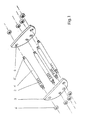
- FIG.1 A holding device which corresponds to the cited prior art is shown in Fig.1 shown.
- the semiconductor wafers (not shown in the drawing) are set in this way can be that on four areas of its outer circumference in a vertical, parallel alignment in one for the respective treatment step required distance must be kept.
- two front or end parts 3 are provided, for example with surfaces are provided for placing the holding device on a base.
- the holding elements 1 are 3 openings on the front and end parts 4 available, with the positions of the spatial arrangement of the holding elements 1 is set.
- the holding elements 1 have threads 5 on both sides at their ends, which together with nuts 6 serve for connection to the front or end parts 3.
- holding devices are known in which the individual device parts are connected by welding or gluing, as for example in JP 08 316 158 A described.
- this may result from the introduction of foreign material the requirements for purity and, when gluing, the stability requirements in the high temperature range.
- the invention lies the task is based on a method of the type mentioned and a to provide the holding device for semiconductor wafers produced by the method, the purity requirements with regard to the device parts and the Part connections used materials and also the mechanical stability of the Part connection up to temperatures of 1,350 ° C are guaranteed.
- Device parts are initially prefabricated individually from single or polycrystalline silicon and provided with matching mating surfaces, then the adjacent device parts with opposing mating surfaces in or joined together and finally the mating surfaces by diffusion welding and / or by soldering, with germanium powder being used as the solder connected.
- the method according to the invention allows the production of a holding device for semiconductor wafers, the highest purity requirements at temperatures up to Corresponds to 1,350 ° C in the clean room; i.e. a release of impurities through the the extent permitted for semiconductor technology is excluded.
- the invention first enables the inexpensive manufacture of individual Parts of the device, especially in the case of geometrically complicated parts is advantageous.
- an inseparable material bond takes place Connection of the device parts with each other, so that a high mechanical and thermal stability of the holding device even under high temperature conditions is guaranteed.
- This has for the temperature range up to 1,350 ° C and the high one Special weight load due to the large number of semiconductor wafers to be accommodated Importance.
- the mating surfaces are preferably made flat, but they can be in any Be arched or curved, of course, which are different Mating surfaces opposite device parts a corresponding one or must have coordinated curvature.
- the diffusion welding is carried out over a period of about three to four hours under a contact pressure of the device parts of up to 10 N / mm 2 and at an ambient temperature of 1000 ° C to 1300 ° C. .
- the device parts are preferably surrounded by atmospheric air during the welding process.
- the device parts are prepared so that the opposing Mating surfaces of two adjacent device parts with respect to their Curvature with one another across the entire area intended for welding touch.
- the mating surfaces can be flat and parallel to each other or be designed with the same curvature so that they are the least Touch gap formation.
- the soldering of the device parts is carried out in such a way that powdered first Germanium with a grain size smaller than 50 ⁇ m in one between the opposing ones Fitting surfaces of two device parts formed gap introduced and then the device parts at a pressure of less than 30 mbar and bonded together at the temperature of 900 ° C to 1350 ° C.
- the germanium acts as a solder.
- germanium powder instead of mere germanium powder, a mixture of germanium powder and high-purity water or a mixture of germanium powder and an organic Oil, for example pine oil, can be used.
- the admixture of water or oil is used to fix the solder and to improve its flowability. The additives disappear from the residue during heating Joining seam and have no adverse effect on their strength.
- Two parts of the device to be connected are used to prepare for soldering compared that a gap width in the size range of 0.1 mm to 0.5 mm remains between the mating surfaces.
- the mating surfaces can also be provided here just train and with a distance within the aforementioned range from 0.1 mm to 0.5 mm, or the mating surfaces trained curved, the curvatures on the two mating surfaces in it is provided that the distance between the mating surfaces of two device parts is not less than 0.1 mm and not more than 0.5 mm.
- the gap width can remain constant over this entire area can be formed or it can also be within this range of 0.1 mm gap width varying between 0.5 mm between the two opposing ones Mating surfaces are provided, which is both for opposite planes curved surfaces can also be the case.
- a Purged with argon This keeps oxygen and one Prevents germanium oxide formation, which adversely affects the strength of the joint would impact.
- the joining seam consists of the same type, in the embodiment according to subclaim 3 of alien, but the silicon chemically similar material that does not allow contamination and also the stability requirements enough.
- the proposed opens up particularly advantageously Connection technology the possibility of repairing holding devices under Maintaining high purity, which was previously not possible with regard to defective parts was. So far, in the case of material breaks in such devices always the new production of at least individual parts necessary.
- the invention further relates to a holding device for semiconductor wafers, which is produced according to the aforementioned process steps.
- the holding device consists of individual parts of the device according to the above Processes are interconnected and between which the semiconductor wafers are recorded with essentially parallel alignment.
- the device parts are equipped with mating surfaces that differ from the device part to face the device part and according to the invention by diffusion welding are fused together or between which germanium is introduced as a solder, two device parts each on their mating surfaces are soldered together.
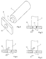
- a cylindrical holding part 7 can be seen in FIG is provided with an end part 8.
- the holding part 7 corresponds to the holding element 1 according to the prior art according to Fig.1.
- the holding part 7 recesses for receiving the semiconductor wafers serve.
- the recesses are not drawn here have been shown again, since their design is principally the representation in Fig. 1 and can also be seen there.
- the holding part 7 has a cylindrical projection 9, the shape and Expansion corresponds to a recess 10 on the end part 8.
- the width of the gap 11 not provided evenly over the entire circumferential surface, but the gap 11 (viewed from the holding part 7) has an increasing gap width, the smallest gap width is 0.1 mm and the largest gap width is 0.5 mm.
- the maximum gap width of 0.5 mm is formed near the transition from the cylindrical extension 9 to the holding part 7, while the gap width decreases with increasing distance from the holding part 7.
- the mating surface on the holding part 7 and / or the mating surface on the shoulder 9 be inclined ", ie run at an angle deviating from 90 ° with respect to the respective base area. It is only important here that the two opposing mating surfaces are inclined towards one another.
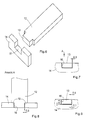
- grooves 17 and / or bevel-like in the mating surfaces Bevels 18 are incorporated, as is the example in FIGS. 3 and 8 is shown. This ensures that the solder has a functionally more favorable distribution can occupy between the mating surfaces.
- FIG. 6 shows a holding part 12 which has a rectangular cross section and is provided with a cuboid extension 13.
- the holding part 12 is for connection provided with a device part 14, the one in terms of their shape and size in the cuboid extension 13 corresponding recess 15 incorporated is.
- FIG. 8 This configuration is shown in FIG. 8 in a view A from FIG. Here too to recognize the constant gap width of the gap 16.
- an embodiment variant of the invention is shown as an example with a non-uniform one Gap width shown between the opposing surfaces.
- the gap width varies in the range from 0.1 mm to 0.5 mm.
- the entire holding device for semiconductor wafers is similar to that in Fig.1 State of the art shown consisting of two plate-shaped or disc-shaped end supports, between which there are several holding elements or parts that are suitable are to accommodate a plurality of semiconductor wafers substantially parallel to the surface.
- holding elements can e.g. Cross-sectional shapes as shown in Fig.2 and Fig.6 have. Further conceivable embodiments of the holding elements are the Circular cylindrical jacket parts adapted to the semiconductor wafers to be accommodated or sections with groove-shaped recesses arranged inside for the fixation of the semiconductor wafers.
- the aforementioned parts of the holding device are made of single or polycrystalline Highest purity silicon.
- the surfaces are machined, partly up to surface polishing.
- the parts are joined by soldering as follows: After thorough Cleaning the device parts will be in the intended position fixed in such a way that a joint with a width of 0.1 to 0.5 mm between two Fitting surfaces remain. Powdered germanium with a grain size is placed in this joint introduced less than 50 microns. Then the device parts at a pressure of 30 mbar heated to a temperature of 900 ° C to 1,350 ° C until all parts have reached this temperature.
- the timing is dependent on the mass or expansion of the parts and is approximately 1.5 hours. After approaching the melting temperature of the germanium (958.5 ° C) this fills the gaps 11, 16 in the pasty or liquid state and, if present, the grooves 17 or those formed by bevels 18 Cavities largely and connects to the fitting parts with the device parts. During the soldering process, argon can be flushed out for oxygen keep away.
- the invention is preferably suitable for producing a holding device for Semiconductor wafers made of silicon in single or polycrystalline form, however, is not limited to this. With a corresponding design, in particular the holding elements it is also possible to include products other than just the semiconductor wafers.
- Tubes made of mono- or polycrystalline silicon can thus advantageously be produced are, for example, an outer diameter of 200mm with a wall thickness of 5mm and the total length is at least 900mm.
- the state technology is not possible for reasons related to production technology, to manufacture such a silicon tube in one piece.
- the method according to the invention can, for example, three pipe sections, each 300mm long be joined to the pipe with a total length of 900 mm. You get due to the permanent connection between these three sections Pipe of the desired total length, which is characterized by high mechanical and thermal Stability distinguishes and also under high temperature conditions (up to approx. 1350 ° C) can be used.
Landscapes
- Engineering & Computer Science (AREA)
- Mechanical Engineering (AREA)
- Container, Conveyance, Adherence, Positioning, Of Wafer (AREA)
Applications Claiming Priority (2)
| Application Number | Priority Date | Filing Date | Title |
|---|---|---|---|
| DE19856468A DE19856468C1 (de) | 1998-11-30 | 1998-11-30 | Verfahren zur Herstellung einer Haltevorrichtung für Halbleiterscheiben |
| DE19856468 | 1998-11-30 |
Publications (1)
| Publication Number | Publication Date |
|---|---|
| EP1006564A1 true EP1006564A1 (fr) | 2000-06-07 |
Family
ID=7890299
Family Applications (1)
| Application Number | Title | Priority Date | Filing Date |
|---|---|---|---|
| EP99123484A Withdrawn EP1006564A1 (fr) | 1998-11-30 | 1999-11-25 | Méthode de fabrication d'un support pour plaquettes semiconductrices et dispositif de support |
Country Status (5)
| Country | Link |
|---|---|
| US (1) | US6276592B1 (fr) |
| EP (1) | EP1006564A1 (fr) |
| JP (1) | JP3223183B2 (fr) |
| KR (1) | KR20000035721A (fr) |
| DE (1) | DE19856468C1 (fr) |
Cited By (2)
| Publication number | Priority date | Publication date | Assignee | Title |
|---|---|---|---|---|
| WO2002003428A2 (fr) | 2000-06-30 | 2002-01-10 | Integrated Materials, Inc. | Support de silicium destine a porter des plaquettes au cours d'un traitement thermique et procede de fabrication |
| US6450346B1 (en) | 2000-06-30 | 2002-09-17 | Integrated Materials, Inc. | Silicon fixtures for supporting wafers during thermal processing |
Families Citing this family (9)
| Publication number | Priority date | Publication date | Assignee | Title |
|---|---|---|---|---|
| US6455395B1 (en) | 2000-06-30 | 2002-09-24 | Integrated Materials, Inc. | Method of fabricating silicon structures including fixtures for supporting wafers |
| US6811040B2 (en) * | 2001-07-16 | 2004-11-02 | Rohm And Haas Company | Wafer holding apparatus |
| US6907666B2 (en) * | 2002-12-24 | 2005-06-21 | Delaware Capital Formation, Inc. | Method of assembly of vehicle body structure |
| DE10301245A1 (de) * | 2003-01-15 | 2004-07-29 | Infineon Technologies Ag | Verfahren zum Bearbeiten eines Werkstücks an einem Werkstückträger |
| US7108315B1 (en) | 2003-10-14 | 2006-09-19 | Delaware Capital Formation, Inc. | Support frame for container trailer |
| US7820939B2 (en) * | 2004-07-27 | 2010-10-26 | The Regents Of The University Of Michigan | Zero-gap laser welding |
| CN2762903Y (zh) * | 2004-12-30 | 2006-03-08 | 鸿富锦精密工业(深圳)有限公司 | 光学元件清洗机构 |
| TWI355524B (en) * | 2005-09-09 | 2012-01-01 | Hon Hai Prec Ind Co Ltd | Medical treatment system of radio frequency identi |
| TWI361469B (en) * | 2007-03-09 | 2012-04-01 | Rohm & Haas Elect Mat | Chemical vapor deposited silicon carbide articles |
Citations (8)
| Publication number | Priority date | Publication date | Assignee | Title |
|---|---|---|---|---|
| US3834349A (en) * | 1971-07-07 | 1974-09-10 | Siemens Ag | Device for holding semiconductor discs during high temperature treatment |
| JPS59130419A (ja) * | 1983-01-17 | 1984-07-27 | Tekunisuko:Kk | 拡散治具等の製法 |
| JPS59167015A (ja) * | 1984-03-05 | 1984-09-20 | Fujitsu Ltd | 石英器具製造方法 |
| EP0144998A2 (fr) * | 1983-12-13 | 1985-06-19 | Allied Corporation | Métaux d'apport pour soudage tendre obtenus par solidification rapide |
| JPH06151571A (ja) * | 1992-11-06 | 1994-05-31 | Toshiba Ceramics Co Ltd | 単結晶シリコン製ウェーハボート |
| US5458688A (en) * | 1993-03-09 | 1995-10-17 | Tokyo Electron Kabushiki Kaisha | Heat treatment boat |
| EP0793260A1 (fr) * | 1996-02-28 | 1997-09-03 | Asahi Glass Company Ltd. | Nacelle verticale pour galettes semi-conductrices |
| EP0884769A1 (fr) * | 1996-02-29 | 1998-12-16 | Tokyo Electron Limited | Nacelle de traitement thermique pour plaquette de semi-conducteur |
Family Cites Families (13)
| Publication number | Priority date | Publication date | Assignee | Title |
|---|---|---|---|---|
| US3644154A (en) * | 1969-06-09 | 1972-02-22 | Ibm | Method of fabricating semiconductor structures with reduced crystallographic defects |
| DE2349512C3 (de) * | 1973-10-02 | 1978-06-08 | Siemens Ag, 1000 Berlin Und 8000 Muenchen | Verfahren zum Herstellen von Halterungen aus Silicium oder Siliciumcarbid für Diffusions- und Temperprozesse |
| DE3419866C2 (de) * | 1984-05-28 | 1986-06-26 | Heraeus Quarzschmelze Gmbh, 6450 Hanau | Trägerhorde aus Quarzglas für scheibenförmige Substrate |
| US4703884A (en) * | 1985-05-20 | 1987-11-03 | The United States Of America As Represented By The United States Department Of Energy | Steel bonded dense silicon nitride compositions and method for their fabrication |
| DE3608559A1 (de) * | 1986-03-14 | 1987-09-17 | Kernforschungsanlage Juelich | Verfahren zum verbinden von formteilen aus sic mit keramik oder metall und zur oberflaechenbehandlung von sisic sowie eine zum verbinden brauchbare legierung |
| DE3907301A1 (de) * | 1989-03-07 | 1990-09-13 | Claus Und Andrea Holm Fa Dr | Vorrichtung zur halterung eines kollektivs von halbleiterscheiben bei thermischen oder chemischen behandlungsschritten und ihre verwendung |
| US5139594A (en) * | 1990-06-26 | 1992-08-18 | The United States Of America As Represented By The United States Department Of Energy | Method for joining ceramic shapes |
| DE4103084A1 (de) * | 1991-02-01 | 1992-08-13 | Wacker Chemitronic | Magazin zur halterung von scheibenfoermigen werkstuecken, insbesondere halbleiterscheiben, bei der nasschemischen oberflaechenbehandlung in fluessigkeitsbaedern |
| US5372298A (en) * | 1992-01-07 | 1994-12-13 | The Regents Of The University Of California | Transient liquid phase ceramic bonding |
| US5447683A (en) * | 1993-11-08 | 1995-09-05 | General Atomics | Braze for silicon carbide bodies |
| JP3650423B2 (ja) | 1994-09-30 | 2005-05-18 | 東芝セラミックス株式会社 | ウエハボート |
| JPH08316158A (ja) | 1995-05-11 | 1996-11-29 | Toshiba Ceramics Co Ltd | 半導体ウエーハボート |
| US5836505A (en) * | 1996-05-07 | 1998-11-17 | Commissariat A L'energie Atomique | Joining by brazing of ceramic materials containing silicon carbide |
-
1998
- 1998-11-30 DE DE19856468A patent/DE19856468C1/de not_active Expired - Lifetime
-
1999
- 1999-11-19 JP JP32961299A patent/JP3223183B2/ja not_active Expired - Fee Related
- 1999-11-25 EP EP99123484A patent/EP1006564A1/fr not_active Withdrawn
- 1999-11-26 KR KR1019990052921A patent/KR20000035721A/ko not_active Withdrawn
- 1999-11-30 US US09/451,177 patent/US6276592B1/en not_active Expired - Fee Related
Patent Citations (8)
| Publication number | Priority date | Publication date | Assignee | Title |
|---|---|---|---|---|
| US3834349A (en) * | 1971-07-07 | 1974-09-10 | Siemens Ag | Device for holding semiconductor discs during high temperature treatment |
| JPS59130419A (ja) * | 1983-01-17 | 1984-07-27 | Tekunisuko:Kk | 拡散治具等の製法 |
| EP0144998A2 (fr) * | 1983-12-13 | 1985-06-19 | Allied Corporation | Métaux d'apport pour soudage tendre obtenus par solidification rapide |
| JPS59167015A (ja) * | 1984-03-05 | 1984-09-20 | Fujitsu Ltd | 石英器具製造方法 |
| JPH06151571A (ja) * | 1992-11-06 | 1994-05-31 | Toshiba Ceramics Co Ltd | 単結晶シリコン製ウェーハボート |
| US5458688A (en) * | 1993-03-09 | 1995-10-17 | Tokyo Electron Kabushiki Kaisha | Heat treatment boat |
| EP0793260A1 (fr) * | 1996-02-28 | 1997-09-03 | Asahi Glass Company Ltd. | Nacelle verticale pour galettes semi-conductrices |
| EP0884769A1 (fr) * | 1996-02-29 | 1998-12-16 | Tokyo Electron Limited | Nacelle de traitement thermique pour plaquette de semi-conducteur |
Non-Patent Citations (2)
| Title |
|---|
| PATENT ABSTRACTS OF JAPAN vol. 008, no. 256 (E - 280) 22 November 1984 (1984-11-22) * |
| PATENT ABSTRACTS OF JAPAN vol. 009, no. 019 (E - 292) 25 January 1985 (1985-01-25) * |
Cited By (4)
| Publication number | Priority date | Publication date | Assignee | Title |
|---|---|---|---|---|
| WO2002003428A2 (fr) | 2000-06-30 | 2002-01-10 | Integrated Materials, Inc. | Support de silicium destine a porter des plaquettes au cours d'un traitement thermique et procede de fabrication |
| WO2002003428A3 (fr) * | 2000-06-30 | 2002-04-11 | Integrated Materials Inc | Support de silicium destine a porter des plaquettes au cours d'un traitement thermique et procede de fabrication |
| US6450346B1 (en) | 2000-06-30 | 2002-09-17 | Integrated Materials, Inc. | Silicon fixtures for supporting wafers during thermal processing |
| EP1297558B1 (fr) * | 2000-06-30 | 2011-04-20 | Integrated Materials, Inc. | Support de silicium destine a porter des plaquettes au cours d'un traitement thermique et procede de fabrication |
Also Published As
| Publication number | Publication date |
|---|---|
| JP3223183B2 (ja) | 2001-10-29 |
| DE19856468C1 (de) | 2000-06-15 |
| US6276592B1 (en) | 2001-08-21 |
| JP2000164668A (ja) | 2000-06-16 |
| KR20000035721A (ko) | 2000-06-26 |
Similar Documents
| Publication | Publication Date | Title |
|---|---|---|
| DE3544812C2 (fr) | ||
| EP0481236B1 (fr) | Pièce formée d'un élément en métal et d'un élément en céramique | |
| DE10030005A1 (de) | Objektiv, insbesondere Projektionsobjektiv in der Halbleiter-Lithographie | |
| DE19856468C1 (de) | Verfahren zur Herstellung einer Haltevorrichtung für Halbleiterscheiben | |
| DE3817369C2 (fr) | ||
| DE102011102843B4 (de) | +Vakuum - Isolierglas mit erhöhter Standfestigkeit und Verfahren zu seiner Herstellung | |
| DE3510414C2 (fr) | ||
| EP0658724A2 (fr) | Chambre de combustion avec garniture céramique | |
| EP0922981A2 (fr) | Corps joints | |
| DE102020118446A1 (de) | Verbindungselement | |
| DE2349012A1 (de) | Verbindungsstecker fuer lichtleitfasern und verfahren zu dessen herstellung | |
| DE69529366T2 (de) | Sinterteil für und Herstellung eines Substrates | |
| DE102019130676B4 (de) | Halterungsvorrichtung mit einem Fixiermechanismus zur lösbaren Fixierung von stiftförmigen Elementen, Halterungsvorrichtungssystem sowie Verwendung der Halterungsvorrichtung | |
| WO2011120481A1 (fr) | Dispositif à module optique et porte-objectif | |
| DE3608484A1 (de) | Verfahren und anordnung zur justierten montage optischer bauteile | |
| DE2354339C3 (de) | Verfahren zum Zusammenbau von Elektronenstrahlerzeugungssystemen | |
| DE19510149C2 (de) | Verbundkeramikstruktur, Verfahren zur Herstellung der Verbundkeramikstruktur und Verwendung von Abstandhaltern in dem Verfahren | |
| DE102022122655A1 (de) | Verfahren zum Herstellen eines elektrischen Energiespeichers sowie Vorrichtung zum Herstellen eines elektrischen Energiespeichers | |
| DE102019209133A1 (de) | Verfahren zum Testen neuer Werkstoffzusammensetzungen für das pulverbettbasierte Laserschmelzen sowie dafür ausgebildete Vorrichtung | |
| DE4300205A1 (de) | Probenhalterung in Kassettenform | |
| WO2014056879A1 (fr) | Dispositif et procédé destinés à transférer un support d'échantillon depuis un dispositif de transport vers un dispositif de balayage | |
| DE102010041532A1 (de) | Verbundbauteil | |
| DE2434090A1 (de) | Verfahren zur herstellung eines elektrodensystems fuer multipole, einschliesslich monopole, insbesondere fuer massenfilter und nach dem verfahren hergestelltes elektrodensystem | |
| DE2008783C3 (de) | Verfahren zum Zusammenbau einer Röntgenröhre | |
| DE3907301A1 (de) | Vorrichtung zur halterung eines kollektivs von halbleiterscheiben bei thermischen oder chemischen behandlungsschritten und ihre verwendung |
Legal Events
| Date | Code | Title | Description |
|---|---|---|---|
| PUAI | Public reference made under article 153(3) epc to a published international application that has entered the european phase |
Free format text: ORIGINAL CODE: 0009012 |
|
| AK | Designated contracting states |
Kind code of ref document: A1 Designated state(s): AT BE CH CY DE DK ES FI FR GB GR IE IT LI LU MC NL PT SE |
|
| AX | Request for extension of the european patent |
Free format text: AL;LT;LV;MK;RO;SI |
|
| 17P | Request for examination filed |
Effective date: 20001111 |
|
| AKX | Designation fees paid |
Free format text: AT BE CH CY DE DK ES FI FR GB GR IE IT LI LU MC NL PT SE |
|
| 17Q | First examination report despatched |
Effective date: 20031222 |
|
| STAA | Information on the status of an ep patent application or granted ep patent |
Free format text: STATUS: THE APPLICATION IS DEEMED TO BE WITHDRAWN |
|
| 18D | Application deemed to be withdrawn |
Effective date: 20040504 |