EP1006582A2 - Dispositif de mémoire à semi-conducteur comprenant une couche de barrIère à l'hydrogène, et sa méthode de fabrication - Google Patents
Dispositif de mémoire à semi-conducteur comprenant une couche de barrIère à l'hydrogène, et sa méthode de fabrication Download PDFInfo
- Publication number
- EP1006582A2 EP1006582A2 EP99123822A EP99123822A EP1006582A2 EP 1006582 A2 EP1006582 A2 EP 1006582A2 EP 99123822 A EP99123822 A EP 99123822A EP 99123822 A EP99123822 A EP 99123822A EP 1006582 A2 EP1006582 A2 EP 1006582A2
- Authority
- EP
- European Patent Office
- Prior art keywords
- insulating film
- protective insulating
- memory device
- semiconductor memory
- capacitor element
- Prior art date
- Legal status (The legal status is an assumption and is not a legal conclusion. Google has not performed a legal analysis and makes no representation as to the accuracy of the status listed.)
- Granted
Links
Images


Classifications
-
- H—ELECTRICITY
- H10—SEMICONDUCTOR DEVICES; ELECTRIC SOLID-STATE DEVICES NOT OTHERWISE PROVIDED FOR
- H10D—INORGANIC ELECTRIC SEMICONDUCTOR DEVICES
- H10D84/00—Integrated devices formed in or on semiconductor substrates that comprise only semiconducting layers, e.g. on Si wafers or on GaAs-on-Si wafers
- H10D84/80—Integrated devices formed in or on semiconductor substrates that comprise only semiconducting layers, e.g. on Si wafers or on GaAs-on-Si wafers characterised by the integration of at least one component covered by groups H10D12/00 or H10D30/00, e.g. integration of IGFETs
- H10D84/82—Integrated devices formed in or on semiconductor substrates that comprise only semiconducting layers, e.g. on Si wafers or on GaAs-on-Si wafers characterised by the integration of at least one component covered by groups H10D12/00 or H10D30/00, e.g. integration of IGFETs of only field-effect components
- H10D84/83—Integrated devices formed in or on semiconductor substrates that comprise only semiconducting layers, e.g. on Si wafers or on GaAs-on-Si wafers characterised by the integration of at least one component covered by groups H10D12/00 or H10D30/00, e.g. integration of IGFETs of only field-effect components of only insulated-gate FETs [IGFET]
- H10D84/834—Integrated devices formed in or on semiconductor substrates that comprise only semiconducting layers, e.g. on Si wafers or on GaAs-on-Si wafers characterised by the integration of at least one component covered by groups H10D12/00 or H10D30/00, e.g. integration of IGFETs of only field-effect components of only insulated-gate FETs [IGFET] comprising FinFETs
-
- H—ELECTRICITY
- H10—SEMICONDUCTOR DEVICES; ELECTRIC SOLID-STATE DEVICES NOT OTHERWISE PROVIDED FOR
- H10B—ELECTRONIC MEMORY DEVICES
- H10B53/00—Ferroelectric RAM [FeRAM] devices comprising ferroelectric memory capacitors
-
- H—ELECTRICITY
- H10—SEMICONDUCTOR DEVICES; ELECTRIC SOLID-STATE DEVICES NOT OTHERWISE PROVIDED FOR
- H10B—ELECTRONIC MEMORY DEVICES
- H10B53/00—Ferroelectric RAM [FeRAM] devices comprising ferroelectric memory capacitors
- H10B53/30—Ferroelectric RAM [FeRAM] devices comprising ferroelectric memory capacitors characterised by the memory core region
-
- H—ELECTRICITY
- H10—SEMICONDUCTOR DEVICES; ELECTRIC SOLID-STATE DEVICES NOT OTHERWISE PROVIDED FOR
- H10D—INORGANIC ELECTRIC SEMICONDUCTOR DEVICES
- H10D84/00—Integrated devices formed in or on semiconductor substrates that comprise only semiconducting layers, e.g. on Si wafers or on GaAs-on-Si wafers
- H10D84/01—Manufacture or treatment
- H10D84/0123—Integrating together multiple components covered by H10D12/00 or H10D30/00, e.g. integrating multiple IGBTs
- H10D84/0126—Integrating together multiple components covered by H10D12/00 or H10D30/00, e.g. integrating multiple IGBTs the components including insulated gates, e.g. IGFETs
- H10D84/0144—Manufacturing their gate insulating layers
-
- H—ELECTRICITY
- H10—SEMICONDUCTOR DEVICES; ELECTRIC SOLID-STATE DEVICES NOT OTHERWISE PROVIDED FOR
- H10W—GENERIC PACKAGES, INTERCONNECTIONS, CONNECTORS OR OTHER CONSTRUCTIONAL DETAILS OF DEVICES COVERED BY CLASS H10
- H10W20/00—Interconnections in chips, wafers or substrates
- H10W20/01—Manufacture or treatment
- H10W20/031—Manufacture or treatment of conductive parts of the interconnections
- H10W20/0698—Local interconnections
-
- H—ELECTRICITY
- H10—SEMICONDUCTOR DEVICES; ELECTRIC SOLID-STATE DEVICES NOT OTHERWISE PROVIDED FOR
- H10D—INORGANIC ELECTRIC SEMICONDUCTOR DEVICES
- H10D1/00—Resistors, capacitors or inductors
- H10D1/60—Capacitors
- H10D1/68—Capacitors having no potential barriers
Definitions
- the present invention relates to a semiconductor memory device and a method for manufacturing the same, and more particularly, relates to a semiconductor memory device including a capacitor film formed of an insulating metal oxide and a method for manufacturing the same.
- the most crucial objective for realization of such semiconductor memory devices is to develop a process capable of integrating a capacitor element on a CMOS integrated circuit without characteristic degradation.
- the semiconductor memory device 500 includes a semiconductor substrate 33 on which a transistor 34 , including source and drain regions 21 and a gate electrode 22 , is formed.
- a first protective insulation film 23 is formed to cover the entire surface of the semiconductor substrate 33 .
- a data storage capacitor element 35 is formed on the first protective insulation film 23 .
- the capacitor element 35 includes a lower electrode 24 , a capacitor film 25 formed of an insulating metal oxide, and an upper electrode 26 .
- a hydrogen barrier layer 27 having the function of an interconnection layer is formed to cover the data storage capacitor element 35 .
- a second protective insulating film 28 is formed to cover the entire surface of the first protective insulation film 23 and the hydrogen barrier layer 27 .
- contact holes 29 partially exposing the upper electrode 26 and a contact hole 30 partially exposing the lower electrode 24 are formed.
- contact holes 31 partially exposing the transistor 34 are formed.
- an interconnection layer 32 connecting the transistor 34 and the capacitor element 35 is formed in a predetermined location.
- the hydrogen barrier layer 27 is formed to cover the capacitor element 35 . Because the hydrogen barrier layer 27 is formed of a material acting as a barrier against hydrogen in the process after the interconnection layer 32 is formed, the hydrogen barrier layer 27 is capable of suppressing the characteristic degradation of the capacitor element 35 caused by the reduction reaction of the capacitor film 25 formed of an insulating metal oxide.
- a resist layer 61 is formed on the second protective insulating film 28 for forming the contact hole 29 through the second protective insulating film 28 and the hydrogen barrier layer 27 formed on the upper electrode 26 formed of platinum.
- the resist layer 61 is then removed using an oxygen plasma.
- a part of the OH bases 62 generated during the removal of the resist layer 61 are decomposed by the catalytic reaction on a surface 26A of the upper electrode 26 .
- active hydrogen 63 is generated.
- the active hydrogen 63 disperses in the upper electrode 26 .
- the hydrogen 63 disperses in the capacitor element 35 .
- the catalytic reaction generating the active hydrogen 63 on the surface 26A of the upper electrode 26 and a surface 24A of the lower electrode 24 inevitably occurs during the removal step of the resist layer 61 using an O 2 plasma after the etching for forming the contact hole 31 to expose the upper electrode 26 and the lower electrode 24 , both formed of platinum, as shown in Figure 8 .
- the conventional semiconductor memory device 500 cannot suppress this catalytic reaction. Therefore, the conventional semiconductor memory device 500 has the problem of creating characteristic degradation of the capacitor element 35 due to the reduction reaction of the capacitor film 25 formed of an insulating metal oxide.
- a semiconductor memory device includes: a semiconductor substrate including a transistor; a first protective insulating film for covering the semiconductor substrate; at least one data storage capacitor element formed on the first protective insulating film; a second protective insulating film for covering the first protective insulating film and the capacitor element; a hydrogen barrier layer; and an interconnection layer for electrically connecting the transistor and the capacitor element, wherein: the capacitor element includes a lower electrode formed on the first protective insulating film, a capacitor film formed on the lower electrode, and an upper electrode formed on the capacitor film, the capacitor film includes an insulating metal oxide, the second protective insulating film has a first contact hole reaching the upper electrode and a second contact hole reaching the lower electrode, and the hydrogen barrier layer is provided in the first and second contact holes, so as not to expose the upper and the lower electrodes.
- the hydrogen barrier layer includes a material which is conductive and does not cause a catalytic reaction generating active hydrogen
- the hydrogen barrier layer includes at least one material selected from the group consisting of titanium nitride, tantalum nitride, iridium oxide, ruthenium oxide and rhodium oxide
- the insulating metal oxide includes at least one material selected from the group consisting of a ferroelectric material having bismuth layered perovskite structure, lead zirconate titanate, strontium barium titanate, or tantalum pentoxide
- the upper electrode and the lower electrode each includes at least one material selected from the group consisting of platinum, iridium, ruthenium, and rhodium.
- a method for manufacturing a semiconductor memory device including the steps of: forming a first protective insulating film for covering a semiconductor substrate including a transistor; forming at least one data storage capacitor element including a lower electrode, a capacitor film formed of an insulating metal oxide, and an upper electrode on the first protective insulating film; forming a second protective insulating film for covering the first protective insulating film and the capacitor element; forming a first contact hole reaching the upper electrode and a second contact hole reaching the lower electrode; forming a hydrogen barrier layer in the first contact hole and in the second contact hole so as not to expose the upper electrode and the lower electrode; forming a resist layer on the second protective insulating film and the hydrogen barrier, and forming a third contact hole reaching the transistor, and forming an interconnection layer for electrically connecting the capacitor element and the transistor.
- the present invention it is possible to suppress the catalytic reaction generating hydrogen on the surface of the upper electrode and of the lower electrode during the resist removal using an oxygen plasma, and preventing the characteristic degradation of the capacitor element due to the reduction reaction of the capacitor film, by lining with the hydrogen barrier layer the inside of the contact holes reaching the upper electrode and the lower electrode.
- the present invention it is also possible to suppress the hydrogen catalytic reaction on the surfaces of the upper electrode and the lower electrode as well as secure a good conductivity at the part the upper electrode and the lower electrode connect to the interconnection layer.
- a catalytic reaction generating hydrogen occurs on the surfaces of the upper electrode and the lower electrode during the removal of the resist layer using an oxygen plasma. According to the present invention, even if the catalytic reaction occurs, it is possible to re-oxidize the capacitor film by heat treatment in an oxygen atmosphere.
- the resist layer is removed using an oxygen plasma. According to the present invention, however, no catalytic reaction occurs on the surfaces of the upper electrode and the lower electrode during this process because the hydrogen barrier layers are already formed to cover the upper electrode and the lower electrode so as not to expose the electrodes during the resist removal. Thus the capacitor film is not reduced.
- the invention described herein makes possible the advantages of providing a semiconductor memory device with a simple structure which has superb characteristics by suppressing the catalytic reaction generating active hydrogen on a platinum surface and thus suppressing the characteristic degradation of a capacitor element due to the reduction reaction of the capacitor film formed of an insulating metal oxide; and a method for manufacturing such a semiconductor memory device.
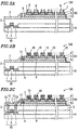
- Figure 1 is a partial cross-sectional view of a semiconductor memory device 100 according to an example of the present invention.
- Figures 2A through 2C are cross-sectional views of the semiconductor memory device 100 , illustrating manufacturing steps thereof.
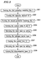
- Figure 3 is a flowchart showing a manufacturing method for a semiconductor memory device 100 .
- the semiconductor memory device 100 includes a semiconductor substrate 41 in which a transistor 42 is formed, a first protective insulating film 3 formed to cover the semiconductor substrate 41 , a data storage capacitor element 43 formed on the first protective insulating film 3 , and a second protective insulating film 7 formed to cover the first protective insulating film 3 and the data storage capacitor element 43 .
- the data storage capacitor element 43 includes a lower electrode 4 formed on the first protective insulating film 3 , a capacitor film 5 formed on the lower electrode 4 , and an upper electrode 6 formed on the capacitor film 5 .
- the capacitor film 5 includes an insulating metal oxide.
- the second protective insulating film 7 has contact holes 8 formed therethrough reaching the upper electrode 6 and a contact hole 9 formed therethrough toward the lower electrode 4 .
- the semiconductor memory device 100 further includes hydrogen barrier layers 10 and 11 respectively lining the contact holes 8 and 9 .
- the hydrogen barrier layer 10 is formed so that the upper electrode 6 is not exposed.
- the hydrogen barrier layer 11 is formed so that the lower electrode 4 is not exposed.
- the semiconductor memory device 100 further includes an interconnection layer 13 for electrically connecting the transistor 42 and the data storage capacitor element 43 .
- the transistor 42 includes source and drain regions 1 and a gate region 2 .
- the first protective insulating film 3 is formed to cover the entire surface of the semiconductor substrate 41 in which the transistor 42 including the source and drain regions 1 and the gate region 2 is formed (S301).
- the lower electrode 4 is formed of platinum on the first protective insulating film 3 by a sputtering method
- the capacitor film 5 is formed of SrBi 2 (Ta 1-x Nb x )O 9 by a metal organic decomposition method or a sputtering method
- the upper electrode 6 is formed of platinum by a sputtering method.
- the lower electrode 4 , the capacitor film 5 , and the upper electrode 6 are processed into the respective predetermined shapes by a dry etching method and thus the data storage capacitor element 43 is formed (S302).
- the second protective insulating film 7 is then formed to cover the entire surface of the first insulating film 3 and the data storage capacitor element 43 (S303). Then, a resist layer (not shown) is formed on the entire surface of the second protective insulating film 7 , and a mask pattern (not shown) for forming the contact holes 8 and 9 are formed on the resist layer by a lithography method. The second protective insulating film 7 is then processed in accordance with the mask pattern to form the contact holes 8 and the contact hole 9 (S304).
- the resist layer is then removed by ashing using an oxygen plasma, and the resultant layers are subsequently heat-treated at 650 °C in an oxygen atmosphere (S305).
- a titanium nitride layer to be the hydrogen barrier layers 10 and 11 is then formed on the entire surface of the resultant layers by a sputtering method.
- a mask pattern (not shown) is formed on the titanium nitride layer by a lithography method so that the hydrogen barrier layers 10 and 11 can be formed to prevent exposure of the upper electrode 6 below the contact holes 8 and the lower electrode 4 below the contact hole 9 .
- the titanium nitride layer is processed in accordance with the mask pattern by a dry etching method to deposit the hydrogen barrier layers 10 lining the contact hole 8 and the hydrogen barrier layer 11 inside the contact hole 9 (S 306).
- a resist layer (not shown) is then formed on the entire surface of the second protective insulating film 7 and the hydrogen barrier layers 10 and 11 , and a mask pattern (not shown) for forming contact holes 12 reaching the transistor 42 is formed on the resist layer by the lithography method.
- the contact holes 12 are then formed by processing the first protective insulating film 3 and the second protective insulating film 7 by a dry etching method according to the mask pattern (S307).
- the resist layer is removed by ashing using an oxygen plasma (S308).
- the interconnection layer 13 is formed by depositing titanium, titanium nitride, aluminum, and titanium nitride in the contact holes 12 and on the second protective insulating film 7 in this order as shown in Figure 2C , in order to electrically connect the data storage capacitor element 43 and the transistor 42 (S309).
- the semiconductor memory device 100 has a plurality of capacitor element portions having respective address numbers A0, A1...An, as shown in Figure 1 .
- the capacitor film 5 can be re-oxidized by heat-treatment in an oxygen atmosphere after the ashing, even if a catalytic reaction generating hydrogen occurs on the surfaces of the upper electrode 6 and the lover electrode 4 when removing the resist layer by ashing using an oxygen plasma after forming the contact holes 8 and 9 . In this manner, the semiconductor memory device 100 is produced.
- the hydrogen barrier layers 10 and 11 are formed to substantially completely cover the contact holes 8 and 9 so as not to expose the upper electrode 6 and the lower electrode 4 when removing the resist layer by ashing using an oxygen plasma after forming the contact holes 12 , no catalytic reaction generating hydrogen occurs on the surfaces of the upper electrode 6 and the lower electrode 4 , and therefore the capacitor films are not reduced.
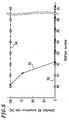
- Figure 4 is a graph comparing the remnant polarization of a capacitor element 43 according to the present invention and of a conventional capacitor element.
- the horizontal axis of the graph represents each of a plurality of address numbers shown in Figure 1 and the vertical axis represents the remnant polarization of the data storage capacitor element 43 .
- the address numbers A0, A1, A2... An are given in sequence from the one nearest to the contact hole 9 above the lower electrode 4 .
- the capacitor element portion having the address number A0 will be referred to as the capacitor element portion A0
- the capacitor element portion having the address number A1 will be referred to as the capacitor element portion A1, and so on.
- the line 51 represents the remnant polarization of the semiconductor 500
- the line 52 represents the remnant polarization of a semiconductor device provided with a hydrogen barrier layer lining the contact holes 8 reaching the upper electrode 6 only
- the line 53 is the remnant polarization of the semiconductor memory device 100 according to the present invention.
- the remnant polarization in all the capacitor element portions A0 through An is about 5 ⁇ C/cm 2 , which indicates significant characteristic degradation. This is because the catalytic reaction occurs on the surface of the upper electrode 6 and the lower electrode 4 , causing the reduction of the capacitor film 5 .
- the characteristic degradation in the capacitor element portions A0 and A1 near the lower electrode 4 is indicated by the decrease of the remnant polarization. This is because hydrogen 63 disperses from the contact hole 9 due to the catalytic reaction on the surface of the lower electrode 4 inside the contact hole 9 , reaching the data storage capacitor element portions A0 and A1, and then the reduction of the capacitor film 5 occurs.
- Figure 5 is a graph comparing the defective bit occurrence rate of a semiconductor device 100 according to the present invention and of a conventional semiconductor device.
- the horizontal axis of the graph represents each of a plurality of address numbers shown in Figure 1 and the vertical axis represents the defective bit occurrence rate.
- the line 54 represents the defective bit occurrence rate of the semiconductor 500
- the line 55 represents the defective bit occurrence rate of a semiconductor device provided with a hydrogen barrier layer only in the contact holes 8 on the upper electrode 6
- the line 56 is the defective bit occurrence rate of the semiconductor memory device 100 according to the present invention.
- all the capacitor element portions A0 through An show a 100% defective bit occurrence rate due to the significant characteristic degradation indicated by the decrease of the remnant polarization.
- defects occur in the capacitor element portions A0 and A1 near the contact hole 9 reaching the lower electrode 4 .
- a defect rate of 0% is achieved in all the capacitor element portions A0 through An.
- Figure 5 shows the performance of the capacitor elements shown in Figure 4 .
- the heat treatment after the ashing is performed at 650°C in an oxygen atmosphere
- the present invention is not limited to this condition. As long as the temperature is within the range of 600 to 850°C, oxidization of the capacitor film is possible, so as to obtain a similar effect.
- titanium nitride is employed for the hydrogen barrier layers 10 and 11
- the present invention is not limited to this material.
- a similar effect is achieved as long as a material not causing a catalytic reaction generating hydrogen and having good conductivity, such as either tantalum nitride, iridium oxide, rutheniumn oxide, or rhodium oxide is used, or at least two of these materials are deposited sequentially.
- SrBi 2 (Ta 1-x Nb x )O 9 is employed for the capacitor film 5
- the present invention is not limited to this material.
- ferroelectric materials having bithmus layered perovskite structure, lead zirconate titanate, strontium barium titanate, or tantalum pentoxide are employed for the capacitor film 5 .
- platinum is employed as the upper electrode 6 and the lower electrode 4 , the present invention is not limited to this material.
- a similar effect is obtained by using an electrode including a deposition layer having either iridium, ruthenium, or rhodium, or a combination thereof.
- the catalytic reaction generating hydrogen on the surface of the upper electrode and the lower electrode occurring during removal of the resist layer using an oxygen plasma is suppressed, which alleviates the characteristic degradation due to the reduction reaction of the capacitor film. Therefore, it is possible to obtain a semiconductor memory device having a better characteristics by an simpler method.
Landscapes
- Semiconductor Memories (AREA)
- Non-Volatile Memory (AREA)
Applications Claiming Priority (2)
| Application Number | Priority Date | Filing Date | Title |
|---|---|---|---|
| JP34389698 | 1998-12-03 | ||
| JP34389698 | 1998-12-03 |
Publications (3)
| Publication Number | Publication Date |
|---|---|
| EP1006582A2 true EP1006582A2 (fr) | 2000-06-07 |
| EP1006582A3 EP1006582A3 (fr) | 2001-06-20 |
| EP1006582B1 EP1006582B1 (fr) | 2008-01-23 |
Family
ID=18365085
Family Applications (2)
| Application Number | Title | Priority Date | Filing Date |
|---|---|---|---|
| EP99120841A Withdrawn EP1006580A3 (fr) | 1998-12-03 | 1999-10-25 | Dispositif de mémoire à semi-conducteur comprenant une couche de barrIère à l'hydrogène, et sa méthode de fabrication |
| EP99123822A Expired - Lifetime EP1006582B1 (fr) | 1998-12-03 | 1999-12-01 | Dispositif de mémoire à semi-conducteur comprenant une couche de barrière à l'hydrogène et sa méthode de fabrication |
Family Applications Before (1)
| Application Number | Title | Priority Date | Filing Date |
|---|---|---|---|
| EP99120841A Withdrawn EP1006580A3 (fr) | 1998-12-03 | 1999-10-25 | Dispositif de mémoire à semi-conducteur comprenant une couche de barrIère à l'hydrogène, et sa méthode de fabrication |
Country Status (6)
| Country | Link |
|---|---|
| US (2) | US6326671B1 (fr) |
| EP (2) | EP1006580A3 (fr) |
| KR (1) | KR100702735B1 (fr) |
| CN (2) | CN1257311A (fr) |
| DE (1) | DE69938030T2 (fr) |
| TW (1) | TW434877B (fr) |
Cited By (2)
| Publication number | Priority date | Publication date | Assignee | Title |
|---|---|---|---|---|
| US7276300B2 (en) | 2001-05-03 | 2007-10-02 | Infineon Technologies Ag | Microelectronic structure having a hydrogen barrier layer |
| US8247323B2 (en) | 2005-10-07 | 2012-08-21 | Fujitsu Semiconductor Limited | Semiconductor device |
Families Citing this family (11)
| Publication number | Priority date | Publication date | Assignee | Title |
|---|---|---|---|---|
| KR100362189B1 (ko) * | 1999-12-30 | 2002-11-23 | 주식회사 하이닉스반도체 | 수소 확산을 방지할 수 있는 산화막 및 티타늄막 이중층을구비하는 반도체 메모리 소자 및 그 제조 방법 |
| US20030224536A1 (en) * | 2002-06-04 | 2003-12-04 | Andreas Hilliger | Contact formation |
| US7161793B2 (en) * | 2002-11-14 | 2007-01-09 | Fujitsu Limited | Layer capacitor element and production process as well as electronic device |
| JP4500262B2 (ja) * | 2003-09-05 | 2010-07-14 | 富士通セミコンダクター株式会社 | 半導体装置及びその製造方法 |
| US7082052B2 (en) * | 2004-02-06 | 2006-07-25 | Unity Semiconductor Corporation | Multi-resistive state element with reactive metal |
| US20060171200A1 (en) | 2004-02-06 | 2006-08-03 | Unity Semiconductor Corporation | Memory using mixed valence conductive oxides |
| JP4904671B2 (ja) * | 2004-06-24 | 2012-03-28 | 日本電気株式会社 | 半導体装置、その製造方法及び電子機器 |
| US20130082232A1 (en) | 2011-09-30 | 2013-04-04 | Unity Semiconductor Corporation | Multi Layered Conductive Metal Oxide Structures And Methods For Facilitating Enhanced Performance Characteristics Of Two Terminal Memory Cells |
| JP4997757B2 (ja) * | 2005-12-20 | 2012-08-08 | 富士通株式会社 | 薄膜キャパシタ及びその製造方法、電子装置並びに回路基板 |
| US7768050B2 (en) * | 2006-07-07 | 2010-08-03 | The Trustees Of The University Of Pennsylvania | Ferroelectric thin films |
| US8354751B2 (en) * | 2008-06-16 | 2013-01-15 | International Business Machines Corporation | Interconnect structure for electromigration enhancement |
Family Cites Families (9)
| Publication number | Priority date | Publication date | Assignee | Title |
|---|---|---|---|---|
| JPH0773104B2 (ja) * | 1986-02-14 | 1995-08-02 | 富士通株式会社 | レジスト剥離方法 |
| JP3319869B2 (ja) * | 1993-06-24 | 2002-09-03 | 三菱電機株式会社 | 半導体記憶装置およびその製造方法 |
| DE69433245T2 (de) * | 1993-08-05 | 2004-07-22 | Matsushita Electric Industrial Co., Ltd., Kadoma | Herstellungsverfahren für Halbleiterbauelement mit Kondensator von hoher dielektrischer Konstante |
| JPH07142597A (ja) * | 1993-11-12 | 1995-06-02 | Mitsubishi Electric Corp | 半導体記憶装置およびその製造方法 |
| JP3119997B2 (ja) * | 1994-06-21 | 2000-12-25 | 松下電子工業株式会社 | 半導体装置の製造方法 |
| JP3417167B2 (ja) * | 1995-09-29 | 2003-06-16 | ソニー株式会社 | 半導体メモリ素子のキャパシタ構造及びその形成方法 |
| EP0837504A3 (fr) * | 1996-08-20 | 1999-01-07 | Ramtron International Corporation | Dispositif ferroélectrique partiellement ou complètement encapsulé |
| JP3028080B2 (ja) | 1997-06-18 | 2000-04-04 | 日本電気株式会社 | 半導体装置の構造およびその製造方法 |
| JPH1118360A (ja) | 1997-06-27 | 1999-01-22 | Shibaura Eng Works Co Ltd | 電動機 |
-
1999
- 1999-10-20 TW TW088118140A patent/TW434877B/zh not_active IP Right Cessation
- 1999-10-25 EP EP99120841A patent/EP1006580A3/fr not_active Withdrawn
- 1999-11-30 KR KR1019990053695A patent/KR100702735B1/ko not_active Expired - Fee Related
- 1999-11-30 CN CN99122843A patent/CN1257311A/zh active Pending
- 1999-12-01 EP EP99123822A patent/EP1006582B1/fr not_active Expired - Lifetime
- 1999-12-01 DE DE69938030T patent/DE69938030T2/de not_active Expired - Lifetime
- 1999-12-01 US US09/452,620 patent/US6326671B1/en not_active Expired - Fee Related
- 1999-12-03 CN CN99127744A patent/CN1126175C/zh not_active Expired - Fee Related
-
2001
- 2001-10-10 US US09/974,510 patent/US6528365B2/en not_active Expired - Fee Related
Cited By (2)
| Publication number | Priority date | Publication date | Assignee | Title |
|---|---|---|---|---|
| US7276300B2 (en) | 2001-05-03 | 2007-10-02 | Infineon Technologies Ag | Microelectronic structure having a hydrogen barrier layer |
| US8247323B2 (en) | 2005-10-07 | 2012-08-21 | Fujitsu Semiconductor Limited | Semiconductor device |
Also Published As
| Publication number | Publication date |
|---|---|
| US20020029373A1 (en) | 2002-03-07 |
| US6528365B2 (en) | 2003-03-04 |
| DE69938030T2 (de) | 2009-01-08 |
| TW434877B (en) | 2001-05-16 |
| CN1257311A (zh) | 2000-06-21 |
| KR100702735B1 (ko) | 2007-04-03 |
| EP1006580A3 (fr) | 2001-06-20 |
| EP1006582A3 (fr) | 2001-06-20 |
| EP1006580A2 (fr) | 2000-06-07 |
| US6326671B1 (en) | 2001-12-04 |
| KR20000047773A (ko) | 2000-07-25 |
| DE69938030D1 (de) | 2008-03-13 |
| EP1006582B1 (fr) | 2008-01-23 |
| CN1126175C (zh) | 2003-10-29 |
| CN1257310A (zh) | 2000-06-21 |
Similar Documents
| Publication | Publication Date | Title |
|---|---|---|
| US6756282B2 (en) | Semiconductor device and method of fabricating the same | |
| US6730951B2 (en) | Capacitor, semiconductor memory device, and method for manufacturing the same | |
| US7456454B2 (en) | Ferroelectric semiconductor device and method of manufacturing the same | |
| JPH0794600A (ja) | 半導体装置およびその製造方法 | |
| US6130124A (en) | Methods of forming capacitor electrodes having reduced susceptibility to oxidation | |
| US7221013B2 (en) | Semiconductor device | |
| JPH11126881A (ja) | 高強誘電体薄膜コンデンサを有する半導体装置及びその製造方法 | |
| EP1006582B1 (fr) | Dispositif de mémoire à semi-conducteur comprenant une couche de barrière à l'hydrogène et sa méthode de fabrication | |
| JP3643091B2 (ja) | 半導体記憶装置及びその製造方法 | |
| JP2003068993A (ja) | 半導体装置およびその製造方法 | |
| KR100269331B1 (ko) | 고유전체막을 구비하는 커패시터 형성방법 | |
| JP3166746B2 (ja) | キャパシタ及びその製造方法 | |
| JP2000174213A (ja) | 半導体装置及びその製造方法 | |
| JP3400964B2 (ja) | 半導体記憶装置の製造方法 | |
| KR20030074439A (ko) | 용량소자의 제조방법 | |
| JP4002882B2 (ja) | 容量素子、半導体記憶装置及びその製造方法 | |
| KR100474589B1 (ko) | 캐패시터제조방법 | |
| JPWO2005081317A1 (ja) | 半導体装置の製造方法 | |
| JP3967315B2 (ja) | 容量素子、半導体記憶装置及びその製造方法 | |
| JP2007534139A (ja) | 強誘電体コンデンサのための回復アニールを可能にする多層障壁 | |
| KR100801202B1 (ko) | 반도체 장치의 제조 방법 | |
| JP2007103769A (ja) | 半導体装置 | |
| KR20030054029A (ko) | 반도체 소자의 캐패시터의 제조 방법 | |
| KR20010018060A (ko) | 강유전체 커패시터의 상부 전극을 노출하는 콘택홀 형성방법 |
Legal Events
| Date | Code | Title | Description |
|---|---|---|---|
| PUAI | Public reference made under article 153(3) epc to a published international application that has entered the european phase |
Free format text: ORIGINAL CODE: 0009012 |
|
| AK | Designated contracting states |
Kind code of ref document: A2 Designated state(s): DE FR GB IT NL |
|
| AX | Request for extension of the european patent |
Free format text: AL;LT;LV;MK;RO;SI |
|
| PUAL | Search report despatched |
Free format text: ORIGINAL CODE: 0009013 |
|
| AK | Designated contracting states |
Kind code of ref document: A3 Designated state(s): AT BE CH CY DE DK ES FI FR GB GR IE IT LI LU MC NL PT SE |
|
| AX | Request for extension of the european patent |
Free format text: AL;LT;LV;MK;RO;SI |
|
| RIC1 | Information provided on ipc code assigned before grant |
Free format text: 7H 01L 27/115 A, 7H 01L 21/02 B, 7H 01L 21/8246 B, 7H 01L 21/768 B |
|
| RAP1 | Party data changed (applicant data changed or rights of an application transferred) |
Owner name: MATSUSHITA ELECTRIC INDUSTRIAL CO., LTD. |
|
| 17P | Request for examination filed |
Effective date: 20010627 |
|
| AKX | Designation fees paid |
Free format text: DE FR GB IT NL |
|
| RIC1 | Information provided on ipc code assigned before grant |
Ipc: H01L 21/768 20060101ALI20070608BHEP Ipc: H01L 21/8247 20060101ALI20070608BHEP Ipc: H01L 21/02 20060101ALI20070608BHEP Ipc: H01L 27/115 20060101AFI20070608BHEP |
|
| RTI1 | Title (correction) |
Free format text: SEMICONDUCTOR MEMORY DEVICE HAVING A HYDROGEN BARRIER AND METHOD FOR MANUFACTURING THE SAME |
|
| GRAP | Despatch of communication of intention to grant a patent |
Free format text: ORIGINAL CODE: EPIDOSNIGR1 |
|
| GRAS | Grant fee paid |
Free format text: ORIGINAL CODE: EPIDOSNIGR3 |
|
| GRAA | (expected) grant |
Free format text: ORIGINAL CODE: 0009210 |
|
| AK | Designated contracting states |
Kind code of ref document: B1 Designated state(s): DE FR GB IT NL |
|
| REG | Reference to a national code |
Ref country code: GB Ref legal event code: FG4D |
|
| REF | Corresponds to: |
Ref document number: 69938030 Country of ref document: DE Date of ref document: 20080313 Kind code of ref document: P |
|
| RAP2 | Party data changed (patent owner data changed or rights of a patent transferred) |
Owner name: PANASONIC CORPORATION |
|
| PLBE | No opposition filed within time limit |
Free format text: ORIGINAL CODE: 0009261 |
|
| STAA | Information on the status of an ep patent application or granted ep patent |
Free format text: STATUS: NO OPPOSITION FILED WITHIN TIME LIMIT |
|
| 26N | No opposition filed |
Effective date: 20081024 |
|
| NLT2 | Nl: modifications (of names), taken from the european patent patent bulletin |
Owner name: PANASONIC CORPORATION Effective date: 20081119 |
|
| PGFP | Annual fee paid to national office [announced via postgrant information from national office to epo] |
Ref country code: NL Payment date: 20091216 Year of fee payment: 11 |
|
| PGFP | Annual fee paid to national office [announced via postgrant information from national office to epo] |
Ref country code: IT Payment date: 20091216 Year of fee payment: 11 Ref country code: GB Payment date: 20091125 Year of fee payment: 11 Ref country code: FR Payment date: 20091221 Year of fee payment: 11 |
|
| PGFP | Annual fee paid to national office [announced via postgrant information from national office to epo] |
Ref country code: DE Payment date: 20091126 Year of fee payment: 11 |
|
| REG | Reference to a national code |
Ref country code: NL Ref legal event code: V1 Effective date: 20110701 |
|
| GBPC | Gb: european patent ceased through non-payment of renewal fee |
Effective date: 20101201 |
|
| REG | Reference to a national code |
Ref country code: FR Ref legal event code: ST Effective date: 20110831 |
|
| PG25 | Lapsed in a contracting state [announced via postgrant information from national office to epo] |
Ref country code: FR Free format text: LAPSE BECAUSE OF NON-PAYMENT OF DUE FEES Effective date: 20110103 |
|
| REG | Reference to a national code |
Ref country code: DE Ref legal event code: R119 Ref document number: 69938030 Country of ref document: DE Effective date: 20110701 |
|
| PG25 | Lapsed in a contracting state [announced via postgrant information from national office to epo] |
Ref country code: DE Free format text: LAPSE BECAUSE OF NON-PAYMENT OF DUE FEES Effective date: 20110701 Ref country code: GB Free format text: LAPSE BECAUSE OF NON-PAYMENT OF DUE FEES Effective date: 20101201 |
|
| PG25 | Lapsed in a contracting state [announced via postgrant information from national office to epo] |
Ref country code: NL Free format text: LAPSE BECAUSE OF NON-PAYMENT OF DUE FEES Effective date: 20110701 Ref country code: IT Free format text: LAPSE BECAUSE OF NON-PAYMENT OF DUE FEES Effective date: 20101201 |