EP1006655B1 - Circuit de protection pour un semi-conducteur de puissance - Google Patents
Circuit de protection pour un semi-conducteur de puissance Download PDFInfo
- Publication number
- EP1006655B1 EP1006655B1 EP19990123563 EP99123563A EP1006655B1 EP 1006655 B1 EP1006655 B1 EP 1006655B1 EP 19990123563 EP19990123563 EP 19990123563 EP 99123563 A EP99123563 A EP 99123563A EP 1006655 B1 EP1006655 B1 EP 1006655B1
- Authority
- EP
- European Patent Office
- Prior art keywords
- protection circuit
- power semiconductor
- signal
- sensor
- circuit according
- Prior art date
- Legal status (The legal status is an assumption and is not a legal conclusion. Google has not performed a legal analysis and makes no representation as to the accuracy of the status listed.)
- Expired - Lifetime
Links
- 239000004065 semiconductor Substances 0.000 title claims description 28
- 230000003111 delayed effect Effects 0.000 claims description 2
- 238000012544 monitoring process Methods 0.000 claims description 2
- 230000003068 static effect Effects 0.000 claims description 2
- 238000003745 diagnosis Methods 0.000 claims 5
- 230000006870 function Effects 0.000 description 6
- 230000001681 protective effect Effects 0.000 description 1
- 230000009993 protective function Effects 0.000 description 1
Images
Classifications
-
- H—ELECTRICITY
- H03—ELECTRONIC CIRCUITRY
- H03K—PULSE TECHNIQUE
- H03K17/00—Electronic switching or gating, i.e. not by contact-making and –breaking
- H03K17/08—Modifications for protecting switching circuit against overcurrent or overvoltage
- H03K17/082—Modifications for protecting switching circuit against overcurrent or overvoltage by feedback from the output to the control circuit
- H03K17/0822—Modifications for protecting switching circuit against overcurrent or overvoltage by feedback from the output to the control circuit in field-effect transistor switches
-
- H—ELECTRICITY
- H03—ELECTRONIC CIRCUITRY
- H03K—PULSE TECHNIQUE
- H03K17/00—Electronic switching or gating, i.e. not by contact-making and –breaking
- H03K17/18—Modifications for indicating state of switch
-
- H—ELECTRICITY
- H03—ELECTRONIC CIRCUITRY
- H03K—PULSE TECHNIQUE
- H03K17/00—Electronic switching or gating, i.e. not by contact-making and –breaking
- H03K17/08—Modifications for protecting switching circuit against overcurrent or overvoltage
- H03K2017/0806—Modifications for protecting switching circuit against overcurrent or overvoltage against excessive temperature
Definitions
- the invention relates to a protection circuit for a power semiconductor, which has an integrated sensor for monitoring an operating parameter for overloading and for switching off the power semiconductor when reaching or exceeding a predetermined overload value of the operating parameter and displays the shutdown state on a diagnostic output.
- an output signal occurs when the sensor responds based on the overload value of the operating parameter and shuts itself off.
- the overload protection as overtemperature protection or overload protection, is integrated in the power semiconductors and forms a commercially available module with this.
- the disadvantage of such power semiconductors with integrated protection function consists in the fact that the time of shutdown is not known and thus at any time a safety function can be stopped by the shutdown of the power semiconductor.
- the senor at a value of the operating parameter, which is a predetermined amount below the overload value, emits a prewarning signal on the diagnostic output, which differs from the switch-off signal, and that the prewarning signal is fed to a microcontroller, the the control of the power semiconductor continues controlled in a predetermined manner and / or delayed terminated.
- an early information for an expected shutdown of the power semiconductor can be obtained at the diagnostic output, which can be exploited to carry out an emergency function to be performed if necessary.
- the adjustment of the closed state can be effected.
- the sensor can be configured as a temperature sensor or as a load sensor, the thresholds used being the temperature or the current. As a threshold value, a new time specification can also be selected.
- a clocked signal indicates the expected disconnection case and is formed by the sensor and evaluated by the microcontroller, which then takes over its special function in the form of a predetermined control of the power semiconductor.
- the power semiconductor includes a plurality of different sensors that operate on separate diagnostic outputs or a common diagnostic output. It usually does not matter for the microcontroller from which sensor the prewarning signal is emitted.
- the prewarning signals of the sensors are to cause different emergency functions, then the prewarning signals are fed to the microcontroller via separate diagnostic outputs, so that the latter recognizes the origin of the prewarning signals and can accordingly react differently.
- an embodiment may be advantageous, which is characterized in that a controlled in the clock mode power semiconductor with the occurrence of the prewarning signal via the microcontroller preferably limited in time in continuous operation can be controlled and then switched off. If the bathgurteiters controls a motor, this or one of them operated drive mechanism can be brought at full drive of the power semiconductor in overdrive in a defined end position.
- Another advantage is a further development, which is characterized in that the response values for the sensors for emitting a prewarning signal by an external circuit of the power semiconductor is adjustable.
- the protection circuit is then adjustable to different operating data.
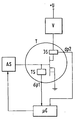
- the specified power semiconductor in the form of a power MOS FET T one is provided with a sensor TS or an overload sensor JS, which is integrated in the power semiconductor and has a diagnostic output dp1 or dp2.
- the power semiconductor may also have integrated several different sensors, as the exemplary embodiment with a temperature sensor TS and an overload sensor shows.
- the power MOS-FET T is an N-channel power MOS-FET, which controls a consumer V, wherein via the drive circuit AS a clock mode or a continuous operation is possible.
- the sensors TS and JS integrated in the power MOS-FET T give a shutdown signal on the diagnostic output dp1 or dp2 when a predetermined overload temperature or overload current is reached or exceeded.
- the signal "1" indicates the switch-off state of the power MOSFET T.
- Both sensors TS and JS can also work on a common diagnostic output. Separate diagnostic outputs dp1 and dp2 are useful if the microcontroller ⁇ C has to respond differently to the prewarning signals that occur.
- An improved protective function for the power MOS-FET T1 is achieved by the sensor or sensors TS, JS an additional threshold which is less than the overload value of the monitored operating parameter.
- an impending disconnection case which is automatically executed at the overload value of the power MOS FET T, will be announced.
- a preferably clocked prewarning signal appears on the diagnostic output dp1 or dp2, which the connected microcontroller .mu.C can easily distinguish from the switch-off duration signal.
- the Miktrocontroller ⁇ C then initiates via the drive circuit AS a controlled shutdown of the power MOS FET T, which can also be made with a certain delay.
- the clocked in the power mode power MOS FET T can also be fully controlled in the pre-warning by the microcontroller ⁇ C and operated in maximum load operation. This is of particular interest when the power MOS FET T controls a motor as a consumer V, which then still has to be brought into a defined end position. In this case, a limit switch of the motor or of the motor-controlled drive or device can be exploited for the final shutdown.
Landscapes
- Semiconductor Integrated Circuits (AREA)
- Emergency Protection Circuit Devices (AREA)
- Protection Of Static Devices (AREA)
Claims (8)
- Circuit de protection pour un semi-conducteur de puissance, comprenant un détecteur intégré pour surveiller un paramètre de fonctionnement du point de vue de la surcharge et pour déconnecter le MOSFET de puissance lorsque l'on atteint ou dépasse une valeur de surcharge prédéterminée du paramètre de fonctionnement et qui affiche l'état de déconnexion sur une sortie de diagnostic,
caractérisé en ce que
le détecteur (TS, JS) émet sur la sortie de diagnostic (dp1, dp2), pour une valeur du paramètre de fonctionnement se situant à un niveau prédéterminé en dessous de la valeur de surcharge, un signal d'avertissement qui se distingue du signal de coupure, et
le signal d'avertissement est envoyé à un microcontrôleur (µC) qui, d'une manière prédéterminée, transmet de façon contrôlée la commande du semi-conducteur de puissance (T) et/ou qui la termine avec retard. - Circuit de protection selon la revendication 1,
caractérisé en ce que
le détecteur (TS) est un capteur de température. - Circuit de protection selon la revendication 1,
caractérisé en ce que
le détecteur (JS) est un capteur de charge. - Circuit de protection selon l'une quelconque des revendications 1 à 3,
caractérisé en ce qu'
à l'état de repos et à l'état déconnecté du détecteur (TS, JS), il y a des signaux statiques différents ("0" et "1") sur la sortie de diagnostic (dp1, dp2), et
un signal cadencé est présent en guise de signal d'avertissement. - Circuit de protection selon l'une quelconque des revendications 1 à 4,
caractérisé en ce que
le semi-conducteur de puissance (T) contient plusieurs détecteurs (TS et JS) différents, qui travaillent sur des sorties de diagnostic séparées (dp1, dp2) ou sur une sortie de diagnostic commune. - Circuit de protection selon l'une quelconque des revendications 1 à 5,
caractérisé en ce qu'
un semi-conducteur de puissance commandé en fonctionnement cadencé peut être commandé en fonctionnement permanent de préférence de façon limitée dans le temps et ensuite déconnecté par le microcontrôleur (µC) lors de l'apparition du signal d'avertissement. - Circuit de protection selon la revendication 6,
caractérisé en ce que
le microcontrôleur (µC) termine également une autre commande du semi-conducteur de puissance (T) lors de l'apparition du signal de coupure. - Circuit de protection selon l'une quelconque des revendications 1 à 7,
caractérisé en ce que
les seuils de réponse pour les détecteurs (TS, JS) en vue de l'émission d'un signal d'avertissement sont réglables par une ligne externe du semi-conducteur de puissance (T).
Applications Claiming Priority (2)
| Application Number | Priority Date | Filing Date | Title |
|---|---|---|---|
| DE19855370 | 1998-12-01 | ||
| DE1998155370 DE19855370A1 (de) | 1998-12-01 | 1998-12-01 | Schutzschaltung für einen Leistungshalbleiter |
Publications (3)
| Publication Number | Publication Date |
|---|---|
| EP1006655A2 EP1006655A2 (fr) | 2000-06-07 |
| EP1006655A3 EP1006655A3 (fr) | 2004-06-16 |
| EP1006655B1 true EP1006655B1 (fr) | 2006-03-01 |
Family
ID=7889609
Family Applications (1)
| Application Number | Title | Priority Date | Filing Date |
|---|---|---|---|
| EP19990123563 Expired - Lifetime EP1006655B1 (fr) | 1998-12-01 | 1999-11-26 | Circuit de protection pour un semi-conducteur de puissance |
Country Status (3)
| Country | Link |
|---|---|
| EP (1) | EP1006655B1 (fr) |
| DE (2) | DE19855370A1 (fr) |
| ES (1) | ES2258834T3 (fr) |
Families Citing this family (4)
| Publication number | Priority date | Publication date | Assignee | Title |
|---|---|---|---|---|
| DE10053334B4 (de) | 2000-10-27 | 2018-08-02 | Robert Bosch Gmbh | Verfahren und Vorrichtung zur Steuerung eines Stellelements in einem Fahrzeug |
| DE10213617A1 (de) * | 2002-03-27 | 2003-06-12 | Zf Sachs Ag | Leistungshalbleiterschalteranordnung und Verfahren zum Betreiben einer Leistungshalbleiterschalteranordnung, insbesondere zum Schutz eines Leistungshalbleiters vor einer thermischen Überlastung |
| JP4502177B2 (ja) | 2003-10-14 | 2010-07-14 | ルネサスエレクトロニクス株式会社 | 出力回路 |
| DE102016218599A1 (de) * | 2016-09-27 | 2018-03-29 | Robert Bosch Gmbh | Stromrichter, elektrisches Antriebssystem und Verfahren zum Aufladen eines elektrischen Energiespeichers |
Family Cites Families (7)
| Publication number | Priority date | Publication date | Assignee | Title |
|---|---|---|---|---|
| DD116105A1 (fr) * | 1974-11-14 | 1975-11-05 | ||
| US4628397A (en) * | 1984-06-04 | 1986-12-09 | General Electric Co. | Protected input/output circuitry for a programmable controller |
| DE3931921A1 (de) * | 1989-09-25 | 1991-04-04 | Bodenseewerk Geraetetech | Leistungs-steuereinheit |
| JPH0898505A (ja) * | 1994-09-20 | 1996-04-12 | Mitsubishi Electric Corp | 半導体複合素子およびこの素子を備えたインバータ装置の異常検出方法 |
| DE19640446A1 (de) * | 1996-09-30 | 1998-04-16 | Siemens Ag | Schutzschaltungsanordnung |
| DE19745040C2 (de) * | 1997-02-10 | 2003-03-27 | Daimler Chrysler Ag | Anordnung und Verfahren zum Messen einer Temperatur |
| US5986866A (en) * | 1997-04-11 | 1999-11-16 | Siemens Energy & Automation, Inc. | Solid state overload relay |
-
1998
- 1998-12-01 DE DE1998155370 patent/DE19855370A1/de not_active Ceased
-
1999
- 1999-11-26 ES ES99123563T patent/ES2258834T3/es not_active Expired - Lifetime
- 1999-11-26 DE DE59913166T patent/DE59913166D1/de not_active Expired - Lifetime
- 1999-11-26 EP EP19990123563 patent/EP1006655B1/fr not_active Expired - Lifetime
Also Published As
| Publication number | Publication date |
|---|---|
| ES2258834T3 (es) | 2006-09-01 |
| EP1006655A3 (fr) | 2004-06-16 |
| EP1006655A2 (fr) | 2000-06-07 |
| DE19855370A1 (de) | 2000-06-15 |
| DE59913166D1 (de) | 2006-04-27 |
Similar Documents
| Publication | Publication Date | Title |
|---|---|---|
| EP0871579B2 (fr) | Dispositif de commande pour un capteur optique | |
| DE4312865C2 (de) | Antriebseinheit für ein energiebetriebenes Fenster | |
| DE4109867C2 (de) | Schutzeinrichtung für Elektromotoren | |
| DE102018200129B4 (de) | Steuervorrichtung für einen Halbleiterschalter | |
| DE112016001253T5 (de) | Fahrzeugsteuereinrichtung, verfahren zum steuern einer fahrzeugsteuereinrichtung und fahrzeugsteuersystem | |
| EP0100852A1 (fr) | Arrangement d'un circuit pour faire sortir et rentrer une antenne entraînée par un moteur | |
| DE102007050844A1 (de) | Booster-Leistungsschaltkreis | |
| EP2391789A1 (fr) | Circuit de commande pour un entraînement de lève-vitre | |
| DE102005031622A1 (de) | Steuervorrichtung eines Halbleiterschalters | |
| EP0680846B1 (fr) | Appareil électrique de commande pour véhicules, en particulier appareil électronique de commande de freins | |
| DE60024165T2 (de) | Wischersteuervorrichtung | |
| DE2944224C2 (fr) | ||
| EP1006655B1 (fr) | Circuit de protection pour un semi-conducteur de puissance | |
| DE60113610T2 (de) | Wischersteuervorrichtung | |
| EP0780031B1 (fr) | Circuit permettant de faire fonctionner un moteur electrique | |
| EP0556191B2 (fr) | Circuit pour la commande d'un servomoteur | |
| DE69809195T2 (de) | Ein antriebssystem für elektrisch betätigte vorrichtungen, wie türen, fenster und dergleichen, sowie antriebseinheit zur verwendung bei einem derartigen system | |
| DE112020004038T5 (de) | Treibervorrichtung | |
| DE19626818A1 (de) | Temperaturkompensierter Überstromwächter für Gleichstrommotoren | |
| DE19648562C2 (de) | Verfahren und Vorrichtung zur Stromüberwachung für Halbleiterschaltungen | |
| EP4076093B1 (fr) | Entraînement à moteur électrique pour meuble | |
| EP0938766B1 (fr) | Systeme de commande par moteur electrique | |
| DE102005009069A1 (de) | Steuerschaltung einer Leistungs-Halbleiter-Vorrichtung und steuernde integrierte Schaltung | |
| DE10249599B4 (de) | Sicherheitsschaltung für analoge Sensoren | |
| DE19858697A1 (de) | Verfahren und Schaltungsanordnung zur Überwachung des Betriebszustandes einer Last |
Legal Events
| Date | Code | Title | Description |
|---|---|---|---|
| PUAI | Public reference made under article 153(3) epc to a published international application that has entered the european phase |
Free format text: ORIGINAL CODE: 0009012 |
|
| AK | Designated contracting states |
Kind code of ref document: A2 Designated state(s): AT BE CH CY DE DK ES FI FR GB GR IE IT LI LU MC NL PT SE |
|
| AX | Request for extension of the european patent |
Free format text: AL;LT;LV;MK;RO;SI |
|
| PUAL | Search report despatched |
Free format text: ORIGINAL CODE: 0009013 |
|
| AK | Designated contracting states |
Kind code of ref document: A3 Designated state(s): AT BE CH CY DE DK ES FI FR GB GR IE IT LI LU MC NL PT SE |
|
| AX | Request for extension of the european patent |
Extension state: AL LT LV MK RO SI |
|
| 17P | Request for examination filed |
Effective date: 20041216 |
|
| AKX | Designation fees paid |
Designated state(s): DE ES FR GB IT |
|
| GRAP | Despatch of communication of intention to grant a patent |
Free format text: ORIGINAL CODE: EPIDOSNIGR1 |
|
| GRAS | Grant fee paid |
Free format text: ORIGINAL CODE: EPIDOSNIGR3 |
|
| GRAA | (expected) grant |
Free format text: ORIGINAL CODE: 0009210 |
|
| AK | Designated contracting states |
Kind code of ref document: B1 Designated state(s): DE ES FR GB IT |
|
| PG25 | Lapsed in a contracting state [announced via postgrant information from national office to epo] |
Ref country code: IT Free format text: LAPSE BECAUSE OF FAILURE TO SUBMIT A TRANSLATION OF THE DESCRIPTION OR TO PAY THE FEE WITHIN THE PRESCRIBED TIME-LIMIT;WARNING: LAPSES OF ITALIAN PATENTS WITH EFFECTIVE DATE BEFORE 2007 MAY HAVE OCCURRED AT ANY TIME BEFORE 2007. THE CORRECT EFFECTIVE DATE MAY BE DIFFERENT FROM THE ONE RECORDED. Effective date: 20060301 |
|
| REG | Reference to a national code |
Ref country code: GB Ref legal event code: FG4D Free format text: NOT ENGLISH |
|
| REF | Corresponds to: |
Ref document number: 59913166 Country of ref document: DE Date of ref document: 20060427 Kind code of ref document: P |
|
| GBT | Gb: translation of ep patent filed (gb section 77(6)(a)/1977) |
Effective date: 20060601 |
|
| REG | Reference to a national code |
Ref country code: ES Ref legal event code: FG2A Ref document number: 2258834 Country of ref document: ES Kind code of ref document: T3 |
|
| ET | Fr: translation filed | ||
| PLBE | No opposition filed within time limit |
Free format text: ORIGINAL CODE: 0009261 |
|
| STAA | Information on the status of an ep patent application or granted ep patent |
Free format text: STATUS: NO OPPOSITION FILED WITHIN TIME LIMIT |
|
| 26N | No opposition filed |
Effective date: 20061204 |
|
| REG | Reference to a national code |
Ref country code: FR Ref legal event code: PLFP Year of fee payment: 17 |
|
| REG | Reference to a national code |
Ref country code: FR Ref legal event code: PLFP Year of fee payment: 18 |
|
| REG | Reference to a national code |
Ref country code: FR Ref legal event code: PLFP Year of fee payment: 19 |
|
| PGFP | Annual fee paid to national office [announced via postgrant information from national office to epo] |
Ref country code: FR Payment date: 20171124 Year of fee payment: 19 |
|
| PGFP | Annual fee paid to national office [announced via postgrant information from national office to epo] |
Ref country code: ES Payment date: 20171201 Year of fee payment: 19 Ref country code: GB Payment date: 20171124 Year of fee payment: 19 Ref country code: IT Payment date: 20171122 Year of fee payment: 19 |
|
| PGFP | Annual fee paid to national office [announced via postgrant information from national office to epo] |
Ref country code: DE Payment date: 20180125 Year of fee payment: 19 |
|
| REG | Reference to a national code |
Ref country code: DE Ref legal event code: R119 Ref document number: 59913166 Country of ref document: DE |
|
| GBPC | Gb: european patent ceased through non-payment of renewal fee |
Effective date: 20181126 |
|
| PG25 | Lapsed in a contracting state [announced via postgrant information from national office to epo] |
Ref country code: IT Free format text: LAPSE BECAUSE OF NON-PAYMENT OF DUE FEES Effective date: 20181126 Ref country code: FR Free format text: LAPSE BECAUSE OF NON-PAYMENT OF DUE FEES Effective date: 20181130 Ref country code: DE Free format text: LAPSE BECAUSE OF NON-PAYMENT OF DUE FEES Effective date: 20190601 |
|
| PG25 | Lapsed in a contracting state [announced via postgrant information from national office to epo] |
Ref country code: GB Free format text: LAPSE BECAUSE OF NON-PAYMENT OF DUE FEES Effective date: 20181126 |
|
| REG | Reference to a national code |
Ref country code: ES Ref legal event code: FD2A Effective date: 20200108 |
|
| PG25 | Lapsed in a contracting state [announced via postgrant information from national office to epo] |
Ref country code: ES Free format text: LAPSE BECAUSE OF NON-PAYMENT OF DUE FEES Effective date: 20181127 |