EP1006765B1 - Verfahren zur Verstärkung von Luftbrücken-Schaltungen - Google Patents
Verfahren zur Verstärkung von Luftbrücken-Schaltungen Download PDFInfo
- Publication number
- EP1006765B1 EP1006765B1 EP99309654A EP99309654A EP1006765B1 EP 1006765 B1 EP1006765 B1 EP 1006765B1 EP 99309654 A EP99309654 A EP 99309654A EP 99309654 A EP99309654 A EP 99309654A EP 1006765 B1 EP1006765 B1 EP 1006765B1
- Authority
- EP
- European Patent Office
- Prior art keywords
- conductor network
- layer
- metal
- resist masks
- apertures
- Prior art date
- Legal status (The legal status is an assumption and is not a legal conclusion. Google has not performed a legal analysis and makes no representation as to the accuracy of the status listed.)
- Expired - Lifetime
Links
Images

Classifications
-
- H—ELECTRICITY
- H05—ELECTRIC TECHNIQUES NOT OTHERWISE PROVIDED FOR
- H05K—PRINTED CIRCUITS; CASINGS OR CONSTRUCTIONAL DETAILS OF ELECTRIC APPARATUS; MANUFACTURE OF ASSEMBLAGES OF ELECTRICAL COMPONENTS
- H05K3/00—Apparatus or processes for manufacturing printed circuits
- H05K3/46—Manufacturing multilayer circuits
- H05K3/4685—Manufacturing of cross-over conductors
-
- H—ELECTRICITY
- H05—ELECTRIC TECHNIQUES NOT OTHERWISE PROVIDED FOR
- H05K—PRINTED CIRCUITS; CASINGS OR CONSTRUCTIONAL DETAILS OF ELECTRIC APPARATUS; MANUFACTURE OF ASSEMBLAGES OF ELECTRICAL COMPONENTS
- H05K3/00—Apparatus or processes for manufacturing printed circuits
- H05K3/02—Apparatus or processes for manufacturing printed circuits in which the conductive material is applied to the surface of the insulating support and is thereafter removed from such areas of the surface which are not intended for current conducting or shielding
- H05K3/06—Apparatus or processes for manufacturing printed circuits in which the conductive material is applied to the surface of the insulating support and is thereafter removed from such areas of the surface which are not intended for current conducting or shielding the conductive material being removed chemically or electrolytically, e.g. by photo-etch process
- H05K3/061—Etching masks
- H05K3/062—Etching masks consisting of metals or alloys or metallic inorganic compounds
-
- H—ELECTRICITY
- H05—ELECTRIC TECHNIQUES NOT OTHERWISE PROVIDED FOR
- H05K—PRINTED CIRCUITS; CASINGS OR CONSTRUCTIONAL DETAILS OF ELECTRIC APPARATUS; MANUFACTURE OF ASSEMBLAGES OF ELECTRICAL COMPONENTS
- H05K3/00—Apparatus or processes for manufacturing printed circuits
- H05K3/10—Apparatus or processes for manufacturing printed circuits in which conductive material is applied to the insulating support in such a manner as to form the desired conductive pattern
- H05K3/20—Apparatus or processes for manufacturing printed circuits in which conductive material is applied to the insulating support in such a manner as to form the desired conductive pattern by affixing prefabricated conductor pattern
- H05K3/205—Apparatus or processes for manufacturing printed circuits in which conductive material is applied to the insulating support in such a manner as to form the desired conductive pattern by affixing prefabricated conductor pattern using a pattern electroplated or electroformed on a metallic carrier
-
- H—ELECTRICITY
- H05—ELECTRIC TECHNIQUES NOT OTHERWISE PROVIDED FOR
- H05K—PRINTED CIRCUITS; CASINGS OR CONSTRUCTIONAL DETAILS OF ELECTRIC APPARATUS; MANUFACTURE OF ASSEMBLAGES OF ELECTRICAL COMPONENTS
- H05K2201/00—Indexing scheme relating to printed circuits covered by H05K1/00
- H05K2201/03—Conductive materials
- H05K2201/0332—Structure of the conductor
- H05K2201/0335—Layered conductors or foils
- H05K2201/0361—Etched tri-metal structure, i.e. metal layers or metal patterns on both sides of a different central metal layer which is later at least partly etched
-
- H—ELECTRICITY
- H05—ELECTRIC TECHNIQUES NOT OTHERWISE PROVIDED FOR
- H05K—PRINTED CIRCUITS; CASINGS OR CONSTRUCTIONAL DETAILS OF ELECTRIC APPARATUS; MANUFACTURE OF ASSEMBLAGES OF ELECTRICAL COMPONENTS
- H05K2201/00—Indexing scheme relating to printed circuits covered by H05K1/00
- H05K2201/03—Conductive materials
- H05K2201/0332—Structure of the conductor
- H05K2201/0388—Other aspects of conductors
- H05K2201/0394—Conductor crossing over a hole in the substrate or a gap between two separate substrate parts
-
- H—ELECTRICITY
- H05—ELECTRIC TECHNIQUES NOT OTHERWISE PROVIDED FOR
- H05K—PRINTED CIRCUITS; CASINGS OR CONSTRUCTIONAL DETAILS OF ELECTRIC APPARATUS; MANUFACTURE OF ASSEMBLAGES OF ELECTRICAL COMPONENTS
- H05K2203/00—Indexing scheme relating to apparatus or processes for manufacturing printed circuits covered by H05K3/00
- H05K2203/03—Metal processing
- H05K2203/0369—Etching selective parts of a metal substrate through part of its thickness, e.g. using etch resist
-
- H—ELECTRICITY
- H05—ELECTRIC TECHNIQUES NOT OTHERWISE PROVIDED FOR
- H05K—PRINTED CIRCUITS; CASINGS OR CONSTRUCTIONAL DETAILS OF ELECTRIC APPARATUS; MANUFACTURE OF ASSEMBLAGES OF ELECTRICAL COMPONENTS
- H05K2203/00—Indexing scheme relating to apparatus or processes for manufacturing printed circuits covered by H05K3/00
- H05K2203/03—Metal processing
- H05K2203/0376—Etching temporary metallic carrier substrate
-
- H—ELECTRICITY
- H05—ELECTRIC TECHNIQUES NOT OTHERWISE PROVIDED FOR
- H05K—PRINTED CIRCUITS; CASINGS OR CONSTRUCTIONAL DETAILS OF ELECTRIC APPARATUS; MANUFACTURE OF ASSEMBLAGES OF ELECTRICAL COMPONENTS
- H05K3/00—Apparatus or processes for manufacturing printed circuits
- H05K3/38—Improvement of the adhesion between the insulating substrate and the metal
- H05K3/386—Improvement of the adhesion between the insulating substrate and the metal by the use of an organic polymeric bonding layer, e.g. adhesive
Definitions
- the present invention relates generally to multilayer circuit boards, and more particularly to multilayer circuit boards having air bridge circuits.
- Air bridge crossover circuits are useful for creating high density circuits. However, such circuits sometimes suffer from susceptibility to mechanical damage, caused by physical impact, thermal excursions, and the like. It would be desirable, therefore, to provide a way of creating such multilayer air bridge circuits without this drawback.
- a multi-layer electronic air bridge crossover circuit assembly made of first, second, and third metals, comprising: (a) a substrate having an electrically insulative surface; (b) a bottom conductor network attached to said electrically insulative surface and comprising a circuit trace and first and second support element pads disposed proximate said circuit trace on opposite sides thereof, said bottom conductor network having a bi-laminate structure comprising (i) a first layer attached to said electrically insulative surface and made of said third metal, and (ii) a second layer attached atop said first layer and made of said second metal; (c) a support element attached atop each support element pad and made of said first metal; (d) a top conductor network including a generally elongate bridging element having first and second enlarged ends and at least one constricted portion therebetween, said bridging element being oriented generally transverse to said circuit trace with each enlarged end thereof attached atop a respective one of the support elements, said top conductor
- a method for additively producing a multi-layer circuit board having air bridge crossovers comprising the steps of: (a) providing a metal foil made of a first metal and having top and bottom foil surfaces; (b) applying first top and bottom plating resist masks to the top and bottom foil surfaces, respectively, wherein the first top and bottom plating resist masks have respective first apertures defined therein corresponding to respective predefined top and bottom conductor patterns; (c) pattern-plating top and bottom conductor networks made of a second metal onto the top and bottom foil surfaces, respectively, through the first apertures in the first top and bottom plating resist masks; (d) applying second top and bottom plating resist masks atop the first top and bottom plating resist masks, respectively, wherein the second masks have respective second apertures defined therein such that each second aperture is at least as large as and is generally centred atop a corresponding one of the first apertures; (e) pattern-plating top and bottom fortifying layers made of a third metal onto the
- a method for subtractively producing a multi-layer circuit board having air bridge crossovers comprising the steps of:(a) providing a multi-layer metal sandwich comprising a central layer made of a first metal and top and bottom conductor network layers made of a second layer attached to respective top and bottom surfaces of the central layer; (b) applying first top and bottom etch resist masks to the top and bottom conductor network layers, respectively, wherein the top and bottom etch resist masks are configured to correspond to respective predefined top and bottom conductor patterns, the first masks further having first apertures defined therein through which exposed portions of the conductor network layers and of the central layer are defined; (c) etching away the exposed portions of the conductor network layers; (d) stripping the first top and bottom etch resist masks, thereby exposing formerly-masked top and bottom conductor network portions, respectively; (e) applying first top and bottom plating resist masks atop the exposed portions of the central layer so as to fill in the etched-away portions of the
- the present invention includes an air bridge circuit having metallic fortifying layers which mechanically and/or electrically enhance the circuit.
- Another advantage is that the present invention may be easily and economically incorporated into both the additive and subtractive air bridge circuit construction processes.
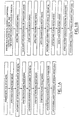
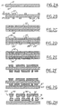
- FIGS. 1A and 2A-H illustrate a first, preferred method for producing a multilayer circuit board having strengthened air bridge crossovers according to the present invention.
- This method involves the steps of: (a) providing a central laver/metal foil 10 made of a first metal and having top and bottom foil surfaces 12/14 (FIG. 2A); (b) applying first top and bottom plating resist masks 22/24 to the top and bottom foil surfaces, respectively, wherein the first top and bottom plating resist masks have respective first apertures 23/25 defined therein corresponding to respective predefined top and bottom conductor patterns (FIG.
- the fortifying layers 52/54 may be made of a metal different from the conductor network layers 32/34 onto which each fortifying layer is plated, or it may be made of the same metal as the fortifying layers.
- This process has the advantage of providing a way of producing generally "T-shaped" (or similarly shaped) air bridge cross-sections as indicated by reference numeral 99 in FIG. 2H.
- Such air bridges with T-shaped or similarly shaped cross-sections are particularly resistant to mechanical stresses caused by bending, flexure, differential thermal expansion, etc., thus providing a mechanically fortified air bridge structure.
- the provision of additional metallic cross-sectional area increases the current-carrying capacity of such bridges, thus providing an electrically fortified bridge structure as well.
- T-shaped bridges 99 are formed by applying two plating resist layers to each side of the circuit -- i.e., first and second top masks 22/26 to the "top" side of the circuit, and first and second bottom masks 24/28 to the "bottom” side of the circuit, as illustrated in FIG. 2D.
- the apertures 23/25/27/29 are sized and arranged such that each first aperture 23/25 has a corresponding second aperture 27/29 generally centered thereatop, with each second aperture being at least as large as -- or optionally larger than -- its corresponding first aperture.
- the resulting air bridge element 99 will have a generally T-shaped (or similarly shaped) cross-section after the masks are stripped and the associated conductor layer portions 32/34 and fortifying layer portions 52/54 are exposed, as illustrated in FIG. 2H.
- T-shaped cross-sections cannot be created using conventional single masks, but require the application of two masks to each side of the circuit, with selected second apertures being sized larger than their corresponding first apertures. This process can be carried out using conventional photoimageable organic masks or similar processes which provide the alignment capabilities required to assure that the second apertures are adequately centered atop their respective first apertures.
- the metals of adjacent layers must be platable/claddable onto each other in the prescribed order (either directly or through optional conversion layers), and (2) the metals must be selectively etchable with respect to each other.
- selectively etchable it is meant that one or more selected metals must be etchable in a given etchant without the etchant appreciably etching the other metals.
- the first, second, and third metals include: (1) aluminum, copper, and nickel, respectively; (2)copper, nickel, and gold, respectively; and (3) steel, copper, and nickel, respectively. Many other combinations of suitable metals are also possible and within the scope of the present invention.
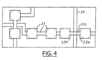
- the bottom conductor network 34 generally comprises a plurality of circuit traces 35 and support element pads 36; typically, the support element pads 36 are arranged in pairs proximate a corresponding circuit trace 35, with one pad 36 on either side of the trace 35.
- the top conductor network 32 comprises at least one bridging element 33 having first and second enlarged ends 33e with at least one constricted portion 33c contiguous with and between (i.e., connecting) the enlarged ends, such as the "dumbbell" shapes illustrated in FIG. 4, and in FIGS. lh and 2c of Livshits.
- Each bridging element 33 is generally oriented transverse to a corresponding circuit trace, with each enlarged end thereof disposed opposite/atop a respective one of the support element pads.
- etching a particular layer
- an etchant be used which etches substantially only the metal of which that particular layer is made.
- the metal foil 10 is to be etched
- the etchant used will etch substantially only the first metal and will not appreciably etch the second and third metals.
- the substrate 60 may be metal, plastic, ceramic, or any other suitable material, with the adhesive 61 being, for example, a thermoset epoxy applied to the substrate.
- the substrate 60 itself may be an adhesive (e.g., thermoset epoxy, thermoplastic resin, etc.) with element 61 simply being an integral surface of the substrate.
- the adhesive/surface 61 be electrically insulative in order to avoid shorts among the bottom conductor network elements.
- FIGS. 1B and 3A-J An alternative, subtractive process embodiment to the foregoing preferred, additive embodiment is illustrated in FIGS. 1B and 3A-J.
- This process comprises the steps of: (a) providing a multilayer metal sandwich comprising a central layer 10 made of a first metal and top and bottom conductor network layers 32/34 made of a second metal attached to respective top and bottom surfaces 12/14 of the central layer 10 (FIG. 3A); (b) applying first top and bottom etch-resist masks 42/44 to the top and bottom conductor network layers, respectively, wherein the top and bottom etch resist masks are configured to correspond to respective predefined top and bottom conductor patterns, the first masks further having first apertures 43/45 defined therein through which exposed portions of the conductor network layers and of the central layer are defined (FIG.
- 2H, 3J, and 4 comprises: (a) a substrate 60 having an electrically insulative surface 61; (b) a bottom conductor network attached to the electrically insulative surface and comprising a circuit trace 35 and first and second support element pads 36 disposed proximate the circuit trace on opposite sides thereof, the bottom conductor network having a bi-laminate structure comprising (b1) a first layer 54 attached to the electrically insulative surface and made of the third metal, and (b2) a second layer 34 attached atop the first layer 54 and made of the second metal; (c) a support element 16 attached atop each support elemenc pad 36 and made of the first metal; (d) a top conductor network including a generally elongate bridging element 33 having first and second enlarged ends 33e and at least one constricted portion 33c therebetween, the bridging element being oriented generally transverse to the circuit trace 35 with each enlarged end thereof attached atop a respective one of the support elements, the top conductor network having a
- electrolytic plating may be a preferred plating method for the plating steps mentioned herein, it is also possible that electroless, immersion, or other methods of plating may also be used.
- pattern-plating and “plating” are variously used herein, methods of metal deposition other than “plating” may alternatively be used and are within the scope of the present invention. Examples of such alternative but equivalent processes include, but are not limited to, sputtering, vacuum metallization/deposition, thermal spraying, dip coating, and the like.
- any reference to “plating” should be construed to include the foregoing approaches and their equivalents.
Landscapes
- Engineering & Computer Science (AREA)
- Manufacturing & Machinery (AREA)
- Microelectronics & Electronic Packaging (AREA)
- Metallurgy (AREA)
- Production Of Multi-Layered Print Wiring Board (AREA)
- Manufacturing Of Printed Wiring (AREA)
- Insulated Metal Substrates For Printed Circuits (AREA)
- Parts Printed On Printed Circuit Boards (AREA)
Claims (10)
- Mehrschichtige elektronische Luftbrückenschaltkreisbaugruppe aus einem ersten, einem zweiten und einem dritten Metall, umfassend:(a) ein Substrat (60) mit einer elektrisch isolierenden Klebstoffoberfläche (61);(b) ein unterseitiges Leiternetz (34), das an der elektrisch isolierenden Oberfläche (61) angebracht ist und eine Leiterbahn (35) und erste und zweite Stützelementinseln (36) umfasst, die nahe der Leiterbahn (35) auf gegenüberliegenden Seiten der Leiterbahn angeordnet sind, wobei das unterseitige Leiternetz (34) eine bi-laminare Struktur aufweist, die folgendes umfasst:(i) eine erste Schicht (54), die an der elektrisch isolierenden Oberfläche (61) angebracht ist und aus dem dritten Metall besteht, und(ii) eine zweite Schicht (34), die auf der ersten Schicht (54) angebracht ist und aus dem zweiten Metall besteht;(c) ein Stützelement (10, 16), das auf jeder Stützelementinsel angebracht ist und aus dem ersten Metall besteht;(d) ein oberseitiges Leitemetz (32) mit einem allgemein länglichen Brückenelement (33), das erste und zweite vergrößerte Enden (33e) und dazwischen wenigstens einen verengten Abschnitt (33c) aufweist, wobei das Brückenelement (33) allgemein quer zu der Leiterbahn ausgerichtet ist, wobei jedes der vergrößerten Enden auf einem jeweiligen Stützelement angebracht ist, wobei das oberseitige Leiternetz (32) eine bi-laminare Struktur aufweist, die folgendes umfasst:(i) eine dritte Schicht (32), die an den Stützelementen angebracht ist und aus dem zweiten Metall besteht, und(ii) eine vierte Schicht (52), die auf der dritten Schicht angebracht ist und aus dem dritten Metall besteht;(e) wobei die vierte Schicht (52) größer bemessen ist als die dritte Schicht (32), dergestalt, dass das Brückenelement (33) einen allgemein T-förmigen Querschnitt (99) aufweist.
- Mehrschichtige elektronische Luftbrückenschaltkreisbaugruppe nach Anspruch 1, wobei es sich bei dem ersten, dem zweiten und dem dritten Metall um folgende Metalle handelt: Aluminium, Nickel bzw. Kupfer; oder Kupfer, Gold bzw. Nickel; oder Stahl, Nickel bzw. Kupfer.
- Verfahren zur additiven Herstellung einer Mehrschichtleiterplatte mit Luftüberbrückungen, wobei das Verfahren folgende Schritte umfasst:(a) Bereitstellen einer Metallfolie (10) aus einem ersten Metall und mit einer Folienober- und einer Folienunterseite (12, 14);(b) Aufbringen von ersten oberseitigen und unterseitigen Galvanisierresistmasken (22, 24) auf die Folienober- bzw. die Folienunterseite, wobei in den ersten oberseitigen und unterseitigen Galvanisierresistmasken jeweilige erste Öffnungen (23, 25) definiert sind, die jeweiligen zuvor festgelegten oberseitigen und unterseitigen Leiterstrukturen entsprechen;(c) Strukturgalvanisieren ober- und unterseitiger Leiternetze (32, 34), die aus einem zweiten Metall bestehen, auf die Folienober- bzw. die Folienunterseite durch die ersten Öffnungen in den ersten oberseitigen und unterseitigen Galvanisierresistmasken hindurch;(d) Aufbringen von zweiten oberseitigen und unterseitigen Galvanisierresistmasken (26, 28) auf die erste oberseitige bzw. unterseitige Galvanisierresistmaske, wobei in den zweiten Masken jeweilige zweite Öffnungen (27, 29) definiert sind, dergestalt, dass jede zweite Öffnung wenigstens so groß ist wie eine entsprechende erste Öffnung und allgemein mittig über einer entsprechenden ersten Öffnung angeordnet ist;(e) Strukturgalvanisieren ober- und unterseitiger Verstärkungsschichten (52, 54), die aus einem dritten Metall bestehen, auf das oberseitigen bzw. unterseitige Leiternetz durch die zweiten Öffnungen hindurch;(f) Ablösen der zweiten oberseitigen und unterseitigen Galvanisierresistmasken (26, 28);(g) Ablösen der ersten oberseitigen und unterseitigen Galvanisierresistmasken (22, 24);(h) Anbringen des unterseitigen Leiternetzes (34) an einem Substrat (60) mittels eines elektrisch isolierenden Klebstoffs (61); und(i) Fortätzen der Metallfolie (10) mit Ausnahme der Abschnitte (16), die sich zwischen dem oberseitigen und dem unterseitigen Leiternetz befinden, wodurch die Luftbrückenstrukturen (90) gebildet werden.
- Verfahren nach Anspruch 3, wobei:das unterseitige Leiternetz eine Leiterbahn und erste und zweite Stützelementinseln umfasst, die nahe der Leiterbahn auf gegenüberliegenden Seiten der Leiterbahn angeordnet sind, unddas oberseitige Leiternetz ein Brückenelement enthält, das erste und zweite vergrößerte Enden und dazwischen wenigstens einen verengten Abschnitt aufweist, wobei das Brückenelement allgemein quer zu der Leiterbahn ausgerichtet ist, wobei jedes der vergrößerten Enden gegenüber einer jeweiligen Stützelementinsel angeordnet ist.
- Verfahren zur subtraktiven Herstellung einer Mehrschichtleiterplatte mit Luftüberbrückungen, wobei das Verfahren folgende Schritte umfasst: (a) Bereitstellen einer Metall-Mehrschichtenstruktur, die eine mittige Schicht (10) aus einem ersten Metall und eine oberseitige und eine unterseitige Leiternetzschicht (32, 34) aus einem zweiten Metall umfasst, die jeweils an einer Oberseite bzw. einer Unterseite (12, 14) der mittleren Schicht befestigt sind;(b) Aufbringen von ersten oberseitigen und unterseitigen Ätzresistmasken (42, 44) auf die oberseitige bzw. die unterseitige Leiternetzschicht, wobei die oberseitigen und unterseitigen Ätzresistmasken so konfiguriert sind, dass sie jeweiligen zuvor festgelegten oberseitigen und unterseitigen Leiterstrukturen entsprechen, wobei die ersten Masken des Weiteren erste Öffnungen (43, 45) aufweisen, durch die freiliegende Abschnitte der Leiternetzschichten und der mittleren Schicht definiert werden;(c) Fortätzen der freiliegenden Abschnitte der Leiternetzschichten (32, 34);(d) Ablösen der ersten oberseitigen und unterseitigen Ätzresistmasken (42, 44), wodurch zuvor maskierte oberseitige bzw. unterseitige Leiternetzabschnitte freigelegt werden;(e) Aufbringen erster oberseitiger und unterseitiger Galvanisierresistmasken (22, 24) auf die freiliegenden Abschnitte der mittleren Schicht, dergestalt, dass die fortgeätzten Abschnitte der Leiternetzschichten im wesentlichen bündig mit den Außenseiten der zuvor maskierten oberseitigen und unterseitigen Leiternetzabschnitte ausgefüllt werden;(f) Aufbringen zweiter oberseitiger und unterseitiger Galvanisierresistmasken (26, 28) auf die ersten oberseitigen bzw. unterseitigen Galvanisierresistmasken, wobei sich in den zweiten oberseitigen und unterseitigen Masken zweite Öffnungen (27, 29) befinden, dergestalt, dass jede zweite Öffnung wenigstens so groß ist wie ein entsprechender oberseitiger oder unterseitiger Leiternetzabschnitt und allgemein mittig über einem entsprechenden oberseitigen oder unterseitigen Leiternetzabschnitt angeordnet ist;(g) Strukturgalvanisieren ober- und unterseitiger Verstärkungsschichten (52, 54), die aus einem dritten Metall bestehen, auf den oberseitigen bzw. unterseitigen Leiternetzabschnitt durch die zweiten Öffnungen hindurch; (h) Ablösen der zweiten oberseitigen und unterseitigen Galvanisierresistmasken (26, 28);(i) Ablösen der ersten oberseitigen und unterseitigen Galvanisierresistmasken (22, 24);(j) Anbringen der unterseitigen Leitemetzabschnitte an einem Substrat (60) mittels eines elektrisch isolierenden Klebstoffs (61); und(k) Fortätzen der mittleren Schicht (10) mit Ausnahme der Abschnitte (16), die sich zwischen dem oberseitigen und dem unterseitigen Leiternetzabschnitt befinden, wodurch Luftbrückenstrukturen (90) gebildet werden.
- Verfahren nach Anspruch 3, 4 oder 5, wobei die Ablöseschritte allgemein gleichzeitig ausgeführt werden.
- Verfahren nach Anspruch 5, wobei wenigstens eine der zweiten Öffnungen größer bemessen ist als ihr entsprechender oberseitiger oder unterseitiger Leiternetzabschnitt.
- Verfahren nach Anspruch 7, wobei die Luftbrückenstruktur, welche der wenigstens einen zweiten Öffnung entspricht, einen allgemein T-förmigen Querschnitt aufweist.
- Verfahren nach Anspruch 5, wobei:die unterseitigen Leiternetzabschnitte eine Leiterbahn und erste und zweite Stützelementinseln umfassen, die nahe der Leiterbahn auf gegenüberliegenden Seiten der Leiterbahn angeordnet sind, unddie oberseitigen Leiternetzabschnitte ein Brückenelement enthalten, das erste und zweite vergrößerte Enden und dazwischen wenigstens einen verengten Abschnitt aufweist, wobei das Brückenelement allgemein quer zu der Leiterbahn ausgerichtet ist, wobei jedes der vergrößerten Enden gegenüber einer jeweiligen Stützelementinsel angeordnet ist.
- Verfahren nach einem der Ansprüche 3 bis 9, wobei es sich bei dem ersten, dem zweiten und dem dritten Metall um folgende Metalle handelt: Aluminium, Nickel bzw. Kupfer; oder Kupfer, Gold bzw. Nickel; oder Stahl, Nickel bzw. Kupfer.
Applications Claiming Priority (2)
| Application Number | Priority Date | Filing Date | Title |
|---|---|---|---|
| US203147 | 1994-02-28 | ||
| US09/203,147 US6217783B1 (en) | 1998-12-01 | 1998-12-01 | Method for strengthening air bridge circuits |
Publications (3)
| Publication Number | Publication Date |
|---|---|
| EP1006765A2 EP1006765A2 (de) | 2000-06-07 |
| EP1006765A3 EP1006765A3 (de) | 2003-01-08 |
| EP1006765B1 true EP1006765B1 (de) | 2004-09-15 |
Family
ID=22752709
Family Applications (1)
| Application Number | Title | Priority Date | Filing Date |
|---|---|---|---|
| EP99309654A Expired - Lifetime EP1006765B1 (de) | 1998-12-01 | 1999-12-01 | Verfahren zur Verstärkung von Luftbrücken-Schaltungen |
Country Status (3)
| Country | Link |
|---|---|
| US (2) | US6217783B1 (de) |
| EP (1) | EP1006765B1 (de) |
| DE (1) | DE69920144T2 (de) |
Families Citing this family (9)
| Publication number | Priority date | Publication date | Assignee | Title |
|---|---|---|---|---|
| US6528736B1 (en) * | 1997-01-21 | 2003-03-04 | Visteon Global Technologies, Inc. | Multi-layer printed circuit board and method of making same |
| JP3371101B2 (ja) * | 2000-02-02 | 2003-01-27 | ティーディーケイ株式会社 | レジストパターンおよびその形成方法、薄膜パターン形成方法ならびにマイクロデバイスの製造方法 |
| US6972379B2 (en) * | 2000-05-26 | 2005-12-06 | Visteon Global Technologies, Inc. | Circuit board and a method for making the same |
| US6449839B1 (en) * | 2000-09-06 | 2002-09-17 | Visteon Global Tech., Inc. | Electrical circuit board and a method for making the same |
| US6454878B1 (en) * | 2000-11-01 | 2002-09-24 | Visteon Global Technologies, Inc. | Cladded material construction for etched-tri-metal circuits |
| US6506062B1 (en) | 2001-08-01 | 2003-01-14 | Visteon Global Technologies, Inc. | Circuit board having an integrated circuit board connector and method of making the same |
| JP4963981B2 (ja) * | 2007-02-19 | 2012-06-27 | 住友電気工業株式会社 | フレキシブルプリント配線板 |
| US8735735B2 (en) * | 2010-07-23 | 2014-05-27 | Ge Embedded Electronics Oy | Electronic module with embedded jumper conductor |
| US9215798B2 (en) * | 2013-03-05 | 2015-12-15 | Eastman Kodak Company | Imprinted multi-layer micro-structure method with multi-level stamp |
Family Cites Families (12)
| Publication number | Priority date | Publication date | Assignee | Title |
|---|---|---|---|---|
| JPS5146904B2 (de) | 1971-09-30 | 1976-12-11 | ||
| US4054484A (en) * | 1975-10-23 | 1977-10-18 | Bell Telephone Laboratories, Incorporated | Method of forming crossover connections |
| NL181611C (nl) * | 1978-11-14 | 1987-09-16 | Philips Nv | Werkwijze ter vervaardiging van een bedradingssysteem, alsmede een halfgeleiderinrichting voorzien van een dergelijk bedradingssysteem. |
| US4289846A (en) * | 1979-12-28 | 1981-09-15 | General Electric Company | Process for forming low-reactance interconnections on semiconductors |
| US4404059A (en) | 1982-05-26 | 1983-09-13 | Livshits Vladimir I | Process for manufacturing panels to be used in microelectronic systems |
| JP2856778B2 (ja) * | 1989-09-07 | 1999-02-10 | 株式会社東芝 | 半導体装置の配線構造 |
| US5219713A (en) * | 1990-12-17 | 1993-06-15 | Rockwell International Corporation | Multi-layer photoresist air bridge fabrication method |
| US5493263A (en) * | 1991-07-19 | 1996-02-20 | Fujitsu Limited | Microstrip which is able to supply DC bias current |
| US5408742A (en) * | 1991-10-28 | 1995-04-25 | Martin Marietta Corporation | Process for making air bridges for integrated circuits |
| JP3359780B2 (ja) * | 1995-04-12 | 2002-12-24 | 三菱電機株式会社 | 配線装置 |
| US5738797A (en) | 1996-05-17 | 1998-04-14 | Ford Global Technologies, Inc. | Three-dimensional multi-layer circuit structure and method for forming the same |
| US6218282B1 (en) * | 1999-02-18 | 2001-04-17 | Advanced Micro Devices, Inc. | Method of forming low dielectric tungsten lined interconnection system |
-
1998
- 1998-12-01 US US09/203,147 patent/US6217783B1/en not_active Expired - Fee Related
-
1999
- 1999-12-01 EP EP99309654A patent/EP1006765B1/de not_active Expired - Lifetime
- 1999-12-01 DE DE69920144T patent/DE69920144T2/de not_active Expired - Fee Related
-
2001
- 2001-01-16 US US09/761,140 patent/US6376780B2/en not_active Expired - Fee Related
Also Published As
| Publication number | Publication date |
|---|---|
| US6217783B1 (en) | 2001-04-17 |
| US6376780B2 (en) | 2002-04-23 |
| DE69920144D1 (de) | 2004-10-21 |
| EP1006765A3 (de) | 2003-01-08 |
| EP1006765A2 (de) | 2000-06-07 |
| DE69920144T2 (de) | 2005-02-03 |
| US20010006115A1 (en) | 2001-07-05 |
Similar Documents
| Publication | Publication Date | Title |
|---|---|---|
| US7211289B2 (en) | Method of making multilayered printed circuit board with filled conductive holes | |
| US4404059A (en) | Process for manufacturing panels to be used in microelectronic systems | |
| US5284548A (en) | Process for producing electrical circuits with precision surface features | |
| US6820330B1 (en) | Method for forming a multi-layer circuit assembly | |
| JP2009135184A (ja) | 配線基板及びその製造方法 | |
| US5442143A (en) | Core for electrical connecting substrates and electrical connecting substrates with core, as well as process for the production thereof | |
| US6162996A (en) | Insulating foil circuit board with rigid and flexible sections | |
| EP1006765B1 (de) | Verfahren zur Verstärkung von Luftbrücken-Schaltungen | |
| KR101019150B1 (ko) | 비아-온-패드 구조를 갖는 인쇄회로기판 제조방법 | |
| KR19980064450A (ko) | 전자 회로에 금속제 스탠드-오프를 형성하는 공정 | |
| US6022466A (en) | Process of plating selective areas on a printed circuit board | |
| US6248247B1 (en) | Method of fortifying an air bridge circuit | |
| KR100720049B1 (ko) | 다층 배선판 및 그 제조 방법 | |
| US6111204A (en) | Bond pads for fine-pitch applications on air bridge circuit boards | |
| US20040168312A1 (en) | PCB with inlaid outerlayer circuits and production methods thereof | |
| US5733468A (en) | Pattern plating method for fabricating printed circuit boards | |
| US6475703B2 (en) | Method for constructing multilayer circuit boards having air bridges | |
| US6293008B1 (en) | Method for producing foil circuit boards | |
| KR100294157B1 (ko) | 다층인쇄회로기판의층간전기접속방법 | |
| US20010004489A1 (en) | Printed circuit boards with solid interconnect and method of producing the same | |
| US6360434B1 (en) | Circuit fabrication | |
| JP4498951B2 (ja) | 配線部材およびフレキシャーの製造方法 | |
| JPH10135640A (ja) | プリント配線板の構造及びその製造方法 | |
| JPH04268783A (ja) | 複合回路基板 | |
| KR20000010059A (ko) | 다층인쇄회로기판의 제조방법 |
Legal Events
| Date | Code | Title | Description |
|---|---|---|---|
| PUAI | Public reference made under article 153(3) epc to a published international application that has entered the european phase |
Free format text: ORIGINAL CODE: 0009012 |
|
| AK | Designated contracting states |
Kind code of ref document: A2 Designated state(s): AT BE CH CY DE DK ES FI FR GB GR IE IT LI LU MC NL PT SE |
|
| AX | Request for extension of the european patent |
Free format text: AL;LT;LV;MK;RO;SI |
|
| PUAL | Search report despatched |
Free format text: ORIGINAL CODE: 0009013 |
|
| AK | Designated contracting states |
Kind code of ref document: A3 Designated state(s): AT BE CH CY DE DK ES FI FR GB GR IE IT LI LU MC NL PT SE |
|
| AX | Request for extension of the european patent |
Free format text: AL;LT;LV;MK;RO;SI |
|
| 17P | Request for examination filed |
Effective date: 20030613 |
|
| AKX | Designation fees paid |
Designated state(s): DE ES GB |
|
| GRAP | Despatch of communication of intention to grant a patent |
Free format text: ORIGINAL CODE: EPIDOSNIGR1 |
|
| GRAS | Grant fee paid |
Free format text: ORIGINAL CODE: EPIDOSNIGR3 |
|
| GRAA | (expected) grant |
Free format text: ORIGINAL CODE: 0009210 |
|
| AK | Designated contracting states |
Kind code of ref document: B1 Designated state(s): DE ES GB |
|
| REG | Reference to a national code |
Ref country code: GB Ref legal event code: FG4D |
|
| REG | Reference to a national code |
Ref country code: IE Ref legal event code: FG4D |
|
| REF | Corresponds to: |
Ref document number: 69920144 Country of ref document: DE Date of ref document: 20041021 Kind code of ref document: P |
|
| PG25 | Lapsed in a contracting state [announced via postgrant information from national office to epo] |
Ref country code: GB Free format text: LAPSE BECAUSE OF NON-PAYMENT OF DUE FEES Effective date: 20041215 |
|
| PG25 | Lapsed in a contracting state [announced via postgrant information from national office to epo] |
Ref country code: ES Free format text: LAPSE BECAUSE OF FAILURE TO SUBMIT A TRANSLATION OF THE DESCRIPTION OR TO PAY THE FEE WITHIN THE PRESCRIBED TIME-LIMIT Effective date: 20041226 |
|
| PG25 | Lapsed in a contracting state [announced via postgrant information from national office to epo] |
Ref country code: DE Free format text: LAPSE BECAUSE OF NON-PAYMENT OF DUE FEES Effective date: 20050701 |
|
| PLBE | No opposition filed within time limit |
Free format text: ORIGINAL CODE: 0009261 |
|
| STAA | Information on the status of an ep patent application or granted ep patent |
Free format text: STATUS: NO OPPOSITION FILED WITHIN TIME LIMIT |
|
| GBPC | Gb: european patent ceased through non-payment of renewal fee |
Effective date: 20041215 |
|
| 26N | No opposition filed |
Effective date: 20050616 |