EP1008002B1 - Metallisches gehäuse mit keramischem einsatzteil für elektronische oder optoelektronische bauelemente - Google Patents
Metallisches gehäuse mit keramischem einsatzteil für elektronische oder optoelektronische bauelemente Download PDFInfo
- Publication number
- EP1008002B1 EP1008002B1 EP98908190A EP98908190A EP1008002B1 EP 1008002 B1 EP1008002 B1 EP 1008002B1 EP 98908190 A EP98908190 A EP 98908190A EP 98908190 A EP98908190 A EP 98908190A EP 1008002 B1 EP1008002 B1 EP 1008002B1
- Authority
- EP
- European Patent Office
- Prior art keywords
- frame
- housing
- housing according
- side walls
- electronic
- Prior art date
- Legal status (The legal status is an assumption and is not a legal conclusion. Google has not performed a legal analysis and makes no representation as to the accuracy of the status listed.)
- Expired - Lifetime
Links
- 239000000919 ceramic Substances 0.000 title claims abstract description 27
- 230000005693 optoelectronics Effects 0.000 title claims abstract description 27
- 229910052751 metal Inorganic materials 0.000 claims abstract description 20
- 239000002184 metal Substances 0.000 claims abstract description 20
- 230000005540 biological transmission Effects 0.000 claims abstract description 17
- 230000003287 optical effect Effects 0.000 claims abstract description 9
- 229910000833 kovar Inorganic materials 0.000 claims description 4
- 239000000463 material Substances 0.000 claims description 4
- FRWYFWZENXDZMU-UHFFFAOYSA-N 2-iodoquinoline Chemical compound C1=CC=CC2=NC(I)=CC=C21 FRWYFWZENXDZMU-UHFFFAOYSA-N 0.000 claims description 2
- 229910000531 Co alloy Inorganic materials 0.000 claims description 2
- RYGMFSIKBFXOCR-UHFFFAOYSA-N Copper Chemical compound [Cu] RYGMFSIKBFXOCR-UHFFFAOYSA-N 0.000 claims description 2
- KGWWEXORQXHJJQ-UHFFFAOYSA-N [Fe].[Co].[Ni] Chemical compound [Fe].[Co].[Ni] KGWWEXORQXHJJQ-UHFFFAOYSA-N 0.000 claims description 2
- LTPBRCUWZOMYOC-UHFFFAOYSA-N beryllium oxide Inorganic materials O=[Be] LTPBRCUWZOMYOC-UHFFFAOYSA-N 0.000 claims description 2
- 229910052802 copper Inorganic materials 0.000 claims description 2
- 239000010949 copper Substances 0.000 claims description 2
- WUUZKBJEUBFVMV-UHFFFAOYSA-N copper molybdenum Chemical compound [Cu].[Mo] WUUZKBJEUBFVMV-UHFFFAOYSA-N 0.000 claims description 2
- SBYXRAKIOMOBFF-UHFFFAOYSA-N copper tungsten Chemical compound [Cu].[W] SBYXRAKIOMOBFF-UHFFFAOYSA-N 0.000 claims description 2
- PMHQVHHXPFUNSP-UHFFFAOYSA-M copper(1+);methylsulfanylmethane;bromide Chemical compound Br[Cu].CSC PMHQVHHXPFUNSP-UHFFFAOYSA-M 0.000 claims description 2
- 229910001092 metal group alloy Inorganic materials 0.000 claims description 2
- 229910001182 Mo alloy Inorganic materials 0.000 claims 1
- 238000004519 manufacturing process Methods 0.000 abstract description 7
- 238000005476 soldering Methods 0.000 description 7
- 239000013307 optical fiber Substances 0.000 description 6
- 238000005219 brazing Methods 0.000 description 4
- 235000021183 entrée Nutrition 0.000 description 4
- 238000000034 method Methods 0.000 description 4
- 239000011324 bead Substances 0.000 description 3
- 239000000470 constituent Substances 0.000 description 3
- 238000013461 design Methods 0.000 description 3
- 238000011161 development Methods 0.000 description 3
- 239000000835 fiber Substances 0.000 description 3
- 238000003780 insertion Methods 0.000 description 3
- 230000037431 insertion Effects 0.000 description 3
- 238000003754 machining Methods 0.000 description 3
- PXHVJJICTQNCMI-UHFFFAOYSA-N Nickel Chemical compound [Ni] PXHVJJICTQNCMI-UHFFFAOYSA-N 0.000 description 2
- 230000015572 biosynthetic process Effects 0.000 description 2
- 238000005520 cutting process Methods 0.000 description 2
- 230000017525 heat dissipation Effects 0.000 description 2
- 239000007769 metal material Substances 0.000 description 2
- 240000008042 Zea mays Species 0.000 description 1
- 238000010276 construction Methods 0.000 description 1
- 230000009977 dual effect Effects 0.000 description 1
- 238000005538 encapsulation Methods 0.000 description 1
- 239000011521 glass Substances 0.000 description 1
- 238000007373 indentation Methods 0.000 description 1
- 239000000203 mixture Substances 0.000 description 1
- 229910052759 nickel Inorganic materials 0.000 description 1
- 230000035515 penetration Effects 0.000 description 1
- 238000007747 plating Methods 0.000 description 1
- 238000004663 powder metallurgy Methods 0.000 description 1
- 238000012552 review Methods 0.000 description 1
- 238000007789 sealing Methods 0.000 description 1
- 229910000679 solder Inorganic materials 0.000 description 1
- 238000003466 welding Methods 0.000 description 1
Images
Classifications
-
- G—PHYSICS
- G02—OPTICS
- G02B—OPTICAL ELEMENTS, SYSTEMS OR APPARATUS
- G02B6/00—Light guides; Structural details of arrangements comprising light guides and other optical elements, e.g. couplings
- G02B6/24—Coupling light guides
- G02B6/42—Coupling light guides with opto-electronic elements
- G02B6/4201—Packages, e.g. shape, construction, internal or external details
-
- G—PHYSICS
- G02—OPTICS
- G02B—OPTICAL ELEMENTS, SYSTEMS OR APPARATUS
- G02B6/00—Light guides; Structural details of arrangements comprising light guides and other optical elements, e.g. couplings
- G02B6/24—Coupling light guides
- G02B6/42—Coupling light guides with opto-electronic elements
- G02B6/4201—Packages, e.g. shape, construction, internal or external details
- G02B6/4256—Details of housings
- G02B6/4262—Details of housings characterised by the shape of the housing
- G02B6/4265—Details of housings characterised by the shape of the housing of the Butterfly or dual inline package [DIP] type
-
- G—PHYSICS
- G02—OPTICS
- G02B—OPTICAL ELEMENTS, SYSTEMS OR APPARATUS
- G02B6/00—Light guides; Structural details of arrangements comprising light guides and other optical elements, e.g. couplings
- G02B6/24—Coupling light guides
- G02B6/42—Coupling light guides with opto-electronic elements
- G02B6/4201—Packages, e.g. shape, construction, internal or external details
- G02B6/4251—Sealed packages
-
- G—PHYSICS
- G02—OPTICS
- G02B—OPTICAL ELEMENTS, SYSTEMS OR APPARATUS
- G02B6/00—Light guides; Structural details of arrangements comprising light guides and other optical elements, e.g. couplings
- G02B6/24—Coupling light guides
- G02B6/42—Coupling light guides with opto-electronic elements
- G02B6/4201—Packages, e.g. shape, construction, internal or external details
- G02B6/4266—Thermal aspects, temperature control or temperature monitoring
-
- G—PHYSICS
- G02—OPTICS
- G02B—OPTICAL ELEMENTS, SYSTEMS OR APPARATUS
- G02B6/00—Light guides; Structural details of arrangements comprising light guides and other optical elements, e.g. couplings
- G02B6/24—Coupling light guides
- G02B6/42—Coupling light guides with opto-electronic elements
- G02B6/4201—Packages, e.g. shape, construction, internal or external details
- G02B6/4274—Electrical aspects
Definitions
- the invention relates to a sealed electronic or optoelectronic box intended to receive electronic components and / or circuits.
- Optoelectronic components act as a converter between an optical signal and an electrical signal, or as a converter between an electrical signal and an optical signal, or also act as a repeater on cables or optical fibers to first receive, amplify, then reinject a light signal .
- the development of 1.3 ⁇ m laser heads for short and medium distance fiber optic links still requires the development of more efficient boxes for the encapsulation of these heads.
- connection pins extend in a plane parallel to the plane defined by the bottom or by the cover of the housing.
- the stacking of shaped and shaped ceramic layers leads to the creation of the side walls of the housing.
- One of the walls called the entry wall, includes a tunnel opening obtained by this stack, and which allows the connection of optical fibers to the internal part of the housing.
- Two other walls opposite, those perpendicular to the entry wall include, in the mass, the means of conveying electrical signals, means to which the pins for connection.
- a metal frame for allow the hermetic closure of the case by means of a cover.
- EP-A-514 213 describes two methods of producing a housing.
- a strip is cut from a metal plate. Fold zones are marked or even slightly indented and lights or indentations are carried out, lights or notches which will be for means of routing of optical or electrical transmission signals.
- the strip is then folded back on itself then welded to form the final frame.
- the frame is finally fixed to the bottom.
- the general and complete shape of the housing is cut out in a metal plate. Fold zones are marked or even slightly notches and lights or cuts are made, lights or cuts that will be for means of routing optical transmission signals or electric.
- the strip and the bottom are then folded back on themselves and then welded to form the final complete housing.
- US-A-4,930,857 describes an electronic and optoelectronic metal housing containing a ceramic multilayer component.
- the frame includes at its base a notch rectangular for the passage of the ceramic multilayer component. This component, by elsewhere with all associated electronics, is placed directly on the bottom of the housing and the frame fits on the bottom thus enclosing the component.
- a major drawback of this type of housing arrangement is that although the frame is annular and in one piece, the component remains on the bottom and all electronic part, in particular with its conductive tracks and its electrical contacts, must adapt to the height, always constant, fixed in advance by the notch for this component.
- Another disadvantage is that the flatness of the frame will be difficult to obtain during soldering on the bottom. These deformations will cause a lack of airtightness between the frame and the ceramic component or between the ceramic component and the bottom.
- a housing for optoelectronic components substantially parallelepiped, intended to receive one or more means of transmission signals between the exterior and the components optoelectronics arranged inside, comprising a bottom and an annular frame constituting walls.
- an object of the invention aims at the realization of an electronic box. or optoelectronics eliminating all or part of said drawbacks and endowed, in particular, high shielding capacity allowing improved operation in the field high frequencies.
- a first problem posed is to make a case, the frame of which is in one holding, which adapts to any type of electronics by having openings that can be placed at the base of the case.
- Another problem posed is to produce a housing whose frame is simultaneously metallic, with a perimeter without discontinuities, and is pierced with one or more lights.
- Yet another problem is to produce a housing whose means signal routing are inserted within the frame in one material and monobloc, in order to give the final unit overall mechanical and thermal stability.
- a housing for electronic components or optoelectronic, substantially rectangular rectangle includes a bottom and a rectangle annular metal frame constituting side walls, as well as at least one opening intended to receive a means of conveying electrical transmission signals between the exterior and the components electronic or optoelectronic arranged inside.
- This housing is characterized in that said at least one opening is formed by a notch formed in an overlapping position on one of said walls lateral and on the bottom, said notch simultaneously showing a lateral slice of the bottom thickness and a slice of the thickness at the base of the frame.
- the height of the frame being small, the place to open a light turns out insufficient.
- the choice for the insert thus fell on one or more lower edges of the case.
- a second problem solved is that the insert is only soldered in two of its faces. This insert is thus not constrained in terms of thermal expansion and is finds free to expand towards its two remaining free faces.
- Another problem solved is that the connection pins can easily be directed to the bottom is perpendicular to the bottom.
- the frame is uninterrupted, without weld bead, or corners of folds.
- transmission signals is meant electrical and / or optical signals.
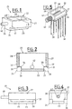
- a housing 21 includes a monobloc frame 22 which has the shape which have generally hermetic box frames: it is of parallelepiped shape rectangle.
- the frame 22, which is continuous, has four side walls. These walls define a periphery which can be lateral exterior, interior lateral, edge upper or lower edge, depending on the angle from which you stand to see it, and which has no discontinuity (connection, ).
- the housing 21 is provided with a bottom 23 whose thickness may be the same or different from that of its side walls by example.
- the material with which the frame is made is a metallic material which can preferably have a coefficient of thermal expansion adapted to that of ceramic used, such as an iron-nickel-cobalt alloy known under the brand name KOVAR® (ASTM F15 standard).
- the frame and the back are made of KOVAR® metal alloy and are hermetically secured by a metal-metal attachment, such as a solder.
- the bottom 23 of the housing 21 can be made of a different metallic material or identical to that used in the production of frame 22 depending on whether it is desired to have of a case with high heat dissipation or not.
- the constituent material of the bottom can preferably be chosen from the group consisting of copper alone, a mixture of copper-tungsten, copper-molybdenum, or beryllium oxide, aluminum nitride, the latter two being at least partially metallized.
- the bottom 23 of the housing 21 may be initially independent of the frame and, in this case, it is attached to the base of the frame, by a metal-to-metal fixing means such that, by example, by soldering, electric reflow or laser. But, the bottom 23 can also be an integral part of the one-piece frame 22 when the structure of the housing 21 is produced by stamping, machining or powder metallurgy. In addition to the frame without discontinuities, we thus constitute a monobloc case, without discontinuities of welds, nor weak areas.
- At least one of the side walls 41 is pierced with a circular tubular opening 42 allowing passage and penetration means for routing optical transmission signals in the form of fibers optics inside the housing 21.
- a tube-shaped element 43 is inserted into the tubular opening 42 and serves to guide and direct the fiber bundle precisely optics to the internal optoelectronic parts of the housing.
- the diameter and height of the orifice 42 on the wall 41 does not condition the final dimensions of the case: there therefore has no costly interventions to plan, for example in a design office and production to adapt the diameter of the tubular opening to the desired dimensions for the case.
- the one-piece frame is provided with an integrated bottom, whose thickness is greater than that of the side walls for example.
- the frame and the integrated bottom constitute a monobloc assembly produced by machining a block of KOVAR®.
- the bottom can also be added by brazing to the base of the frame.
- the metal frame 22 comprises two opposite notches 24, 26 placed in overlapping position on two of the opposite side walls 27, 28 and on the bottom 23.
- the notches simultaneously make visible a side slice 29 of the thickness of the bottom 23 and a slice 31 of the thickness at the base 32 of the frame 22.
- These two notches 24, 26 also show respectively two openings 33, 34.
- These openings 33, 34 are placed in the low position, at the limit of the bottom 23 of the housing 21 and by their positions also have an overlapping location on the walls 27, 28 and the bottom 23. These notches extend over the entire length of the two bottom-wall edges of the housing 21.
- These two notches are intended to receive two multilayer insert elements ceramics 36, 37 serving as means for conveying electrical signals.
- These inserts are hermetically fixed simultaneously to the lateral edge 29 of the thickness of the bottom 23 and at the edge 31 of the thickness at the base 32 of the frame 22, in particular by soldering.
- the notches have a parallelepiped shape corresponding to the shape parallelepiped of the inserts. Therefore, the visible and external edges of the inserts become the edges of the housing 21.
- These ceramic multilayer elements 36, 37 each have conductive via extending in a plane parallel to the side wall of the frame 27, 28.
- Each conductive via provides the electrical connection within the ceramic layers between each internal contact 38 and each external pin 39.
- the pins 39 are located in a plane parallel to the plane defined by the side walls 27, 28 of the frame 22. This allows a new connection to the printed card and a significant saving of space.
- a first method of manufacturing a case for electronic components or optoelectronic, substantially parallelepipedic with a bottom and a constituent frame the walls of the housing and intended to receive one or more means of conveying transmission signals between the exterior and the electronic components or optoelectronics arranged inside includes the steps of cutting transversely a frame in a metal tube having a parallelogram section; drill by machining one or more notches in the frame obtained after cutting, the notches being formed for the subsequent insertion of the means of conveying transmission signals; and fix said frame on the bottom.
- Another method of manufacturing a housing for electronic components or optoelectronic, substantially parallelepipedic with a bottom and a constituent frame the walls of the housing and intended to receive one or more means of conveying transmission signals between the exterior and the electronic components or optoelectronics arranged inside includes the steps of stamping a metal plate to give it a shape similar to a bowl and thus form a draft; machine the blank by leveling the bottom to obtain a frame; punch the frame so as to cut one or more notches, the notch (s) being formed to the subsequent insertion of the means for routing transmission signals; and fix said frame obtained on the merits.
- Yet another method of manufacturing a housing for electronic components or optoelectronic, substantially parallelepipedic with a bottom and a frame constituting the walls of the housing and intended to receive one or more means of transmission signals between the exterior and the components electronic or optoelectronic arranged inside includes the steps of to machine a metal block to give it the final hollow parallelepiped shape of the housing and then punch the notch (s), the notch (s) being made for the subsequent insertion of the means for routing transmission signals.
- the entire housing can be subjected to a partial or total treatment of nickel plating and / or gilding. This treatment can also be made on a box without its inserts or connections.
- the housings according to the invention are not limited by the details of the modes of realization and examples chosen to illustrate them. Changes may be made without departing from the scope of the invention.
- the number of notches in the same wall or within the housing, the corresponding number of inserts ceramics or signal routing means and the dimensions and shapes of all of these cuts may vary. The latter therefore includes all means constituting technical equivalents of the means described as well as their combination.
Landscapes
- Physics & Mathematics (AREA)
- General Physics & Mathematics (AREA)
- Optics & Photonics (AREA)
- Optical Couplings Of Light Guides (AREA)
- Laminated Bodies (AREA)
- Led Device Packages (AREA)
- Ceramic Products (AREA)
- Casings For Electric Apparatus (AREA)
- Semiconductor Lasers (AREA)
- Piezo-Electric Or Mechanical Vibrators, Or Delay Or Filter Circuits (AREA)
Claims (12)
- Gehäuse (21) für elektronische oder optoelektronische Bauteile größtenteils in Form eines rechteckigen Parallelepipeds, das einen Boden (23) und einen rechteckigen, ringförmigen Metallrahmen (22), der Seitenwände (27, 28, 41) bildet, sowie wenigstens eine Öffnung (33, 34) enthält, die dazu dient, eine Einrichtung (36, 37) zum Leiten elektrischer Übertragungssignale zwischen der Außenseite und den elektronischen oder optoelektronischen Bauteilen, die sich im Inneren befinden, aufzunehmen, dadurch gekennzeichnet, dass die wenigstens eine Öffnung (33, 34) durch eine Aussparung (24, 26) gebildet wird, die an einer überlappenden Position an einer der Seitenwände (27, 28) und am Boden (23) ausgebildet ist, wobei die Aussparung sowohl eine seitliche Abschlussfläche (29) der Dicke des Bodens (23) als auch eine Abschlussfläche der Dicke (31) an der Unterseite des Rahmens (32) sichtbar macht.
- Gehäuse nach Anspruch 1, dadurch gekennzeichnet, dass sich die Aussparung (24, 26) über die gesamte Länge einer schneidenden Kante des Gehäuses erstreckt.
- Gehäuse nach Anspruch 1 oder 2, dadurch gekennzeichnet, dass es des Weiteren wenigstens eine Einrichtung zum Leiten elektrischer Übertragungssignale zwischen der Außenseite und den elektronischen oder optoelektronischen Bauteilen, die sich im Inneren befinden, in Form wenigstens eines keramischen Mehrschichtelementes (36, 37) aufweist, das in die Aussparung (24, 26) eingeführt und sowohl an der seitlichen Abschlussfläche (29) der Dicke des Bodens (23) als auch der Abschlussfläche der Dicke an der Unterseite des Rahmens (31) befestigt wird.
- Gehäuse nach Anspruch 3, dadurch gekennzeichnet, dass das wenigstens eine keramische Mehrschichtelement (36, 37) wenigstens eine leitende Durchgangsleitung in einer Ebene parallel zu der Seitenwand (27, 28) des Rahmens aufweist, an der es befestigt ist.
- Gehäuse nach Anspruch 3 oder 4, dadurch gekennzeichnet, dass die Anschlussstifte (39) an der wenigstens einen Einrichtung (36, 37) befestigt sind, um elektrische Übertragungssignale im äußeren Teil des Gehäuses zu leiten, wobei sich die Stifte (39) über den Großteil ihrer Länge in einer Ebene parallel zu der Ebene erstrecken, die durch die Seitenwände (27, 28) des Rahmens gebildet wird.
- Gehäuse nach einem der vorangehenden Ansprüche, dadurch gekennzeichnet, dass es zwei keramische Mehrschichtelemente (36, 37) aufweist, die an zwei einander gegenüberliegenden Seitenwänden (27, 28) befestigt sind.
- Gehäuse nach einem der vorangehenden Ansprüche, dadurch gekennzeichnet, dass wenigstens eine der Seitenwände (41) des Rahmens (22) des Weiteren von einer röhrenförmigen Öffnung (42) für eine Lichtleitereinrichtung zum Leiten von optischen Übertragungssignalen zwischen der Außenseite und den optoelektronischen Bauteilen, die sich im Inneren befinden, durchdrungen wird.
- Gehäuse nach einem der vorangehenden Ansprüche, dadurch gekennzeichnet, dass der Rahmen (22) aus einer Metalllegierung besteht, vorzugsweise einer Eisen-Nickel-Kobalt-Legierung, die als KOVAR® bezeichnet wird.
- Gehäuse nach einem der vorangehenden Ansprüche, dadurch gekennzeichnet, dass der Boden (23) aus dem gleichen Material besteht wie der Rahmen (22).
- Gehäuse nach einem der vorangehenden Ansprüche, dadurch gekennzeichnet, dass der Boden (23) in den Rahmen (22) integriert ist, so dass ein aus einem Stück bestehendes Gehäuse ohne Absätze entsteht.
- Gehäuse nach einem der vorangehenden Ansprüche, dadurch gekennzeichnet, dass der Boden (23) vorzugsweise aus Kupfer, einer Kupfer-Wolfram- oder Kupfer-Molybdän-Legierung, Berylliumoxid oder Aluminiumnitrid besteht.
- Gehäuse nach einem der vorangehenden Ansprüche, dadurch gekennzeichnet, dass der Boden (23) an der Unterseite des Rahmens (22) angebracht ist.
Applications Claiming Priority (3)
| Application Number | Priority Date | Filing Date | Title |
|---|---|---|---|
| FR9702177 | 1997-02-14 | ||
| FR9702177A FR2759847B1 (fr) | 1997-02-14 | 1997-02-14 | Boitier opto-electronique a insert ceramique |
| PCT/FR1998/000284 WO1998036305A1 (fr) | 1997-02-14 | 1998-02-13 | Boitier electronique ou optoelectronique a insert ceramique |
Publications (2)
| Publication Number | Publication Date |
|---|---|
| EP1008002A1 EP1008002A1 (de) | 2000-06-14 |
| EP1008002B1 true EP1008002B1 (de) | 2001-08-29 |
Family
ID=9504103
Family Applications (1)
| Application Number | Title | Priority Date | Filing Date |
|---|---|---|---|
| EP98908190A Expired - Lifetime EP1008002B1 (de) | 1997-02-14 | 1998-02-13 | Metallisches gehäuse mit keramischem einsatzteil für elektronische oder optoelektronische bauelemente |
Country Status (8)
| Country | Link |
|---|---|
| US (1) | US6328483B1 (de) |
| EP (1) | EP1008002B1 (de) |
| JP (1) | JP3342020B2 (de) |
| AT (1) | ATE204992T1 (de) |
| CA (1) | CA2280937C (de) |
| DE (2) | DE69801511T2 (de) |
| FR (1) | FR2759847B1 (de) |
| WO (1) | WO1998036305A1 (de) |
Families Citing this family (11)
| Publication number | Priority date | Publication date | Assignee | Title |
|---|---|---|---|---|
| JP3455168B2 (ja) | 1999-07-19 | 2003-10-14 | 古河電気工業株式会社 | レセプタクルモジュール |
| US6767140B2 (en) * | 2000-05-09 | 2004-07-27 | National Semiconductor Corporation | Ceramic optical sub-assembly for opto-electronic module utilizing LTCC (low-temperature co-fired ceramic) technology |
| US7258839B2 (en) * | 2001-12-21 | 2007-08-21 | Cytonome, Inc. | Temperature controlled microfabricated two-pin liquid sample dispensing system |
| US6846117B2 (en) * | 2002-10-08 | 2005-01-25 | Intel Corporation | Optical module package |
| TWD100417S1 (zh) * | 2003-07-09 | 2004-09-21 | 松下電器產業股份有限公司 | 受光積體電路組件 |
| TWD100418S1 (zh) * | 2003-07-09 | 2004-09-21 | 松下電器產業股份有限公司 | 受光積體電路組件 |
| US7476040B2 (en) * | 2004-02-02 | 2009-01-13 | Jds Uniphase Corporation | Compact optical sub-assembly with ceramic package |
| JP4514647B2 (ja) * | 2005-05-18 | 2010-07-28 | 京セラ株式会社 | 電子部品収納用パッケージおよび電子装置 |
| EP2327122A4 (de) * | 2008-09-15 | 2013-07-24 | Pacific Aerospace & Electronics Inc | Steckverbinderanordnungen mit keramischen einsätzen und leitfähigen pfaden und schnittstellen |
| US9459416B2 (en) * | 2013-01-29 | 2016-10-04 | Kyocera Corporation | Package for housing optical semiconductor element and optical semiconductor device |
| CN116256854B (zh) * | 2023-02-24 | 2026-04-17 | 武汉杉湾新陶瓷材料有限公司 | 一种光通讯管壳结构 |
Family Cites Families (9)
| Publication number | Priority date | Publication date | Assignee | Title |
|---|---|---|---|---|
| US4399541A (en) * | 1981-02-17 | 1983-08-16 | Northern Telecom Limited | Light emitting device package having combined heater/cooler |
| US4930857A (en) * | 1989-05-19 | 1990-06-05 | At&T Bell Laboratories | Hybrid package arrangement |
| JPH03116107A (ja) * | 1989-09-29 | 1991-05-17 | Sumitomo Electric Ind Ltd | 光通信器 |
| US5277357A (en) * | 1991-05-16 | 1994-01-11 | Shinko Electric Industries Co., Ltd. | Process for making a metal wall of a package used for accommodating electronic elements |
| US5416668A (en) * | 1993-11-09 | 1995-05-16 | At&T Corp. | Shielded member |
| US5790730A (en) * | 1994-11-10 | 1998-08-04 | Kravitz; Stanley H. | Package for integrated optic circuit and method |
| US5987205A (en) * | 1996-09-13 | 1999-11-16 | Lutron Electronics Co., Inc. | Infrared energy transmissive member and radiation receiver |
| JP3776191B2 (ja) * | 1997-03-05 | 2006-05-17 | 富士通株式会社 | レセプタクル光モジュール |
| US6056447A (en) * | 1998-04-06 | 2000-05-02 | Lucent Technologies, Inc. | Covariant optical module |
-
1997
- 1997-02-14 FR FR9702177A patent/FR2759847B1/fr not_active Expired - Fee Related
-
1998
- 1998-02-13 WO PCT/FR1998/000284 patent/WO1998036305A1/fr not_active Ceased
- 1998-02-13 EP EP98908190A patent/EP1008002B1/de not_active Expired - Lifetime
- 1998-02-13 JP JP53542798A patent/JP3342020B2/ja not_active Expired - Fee Related
- 1998-02-13 DE DE69801511T patent/DE69801511T2/de not_active Expired - Lifetime
- 1998-02-13 AT AT98908190T patent/ATE204992T1/de active
- 1998-02-13 US US09/367,256 patent/US6328483B1/en not_active Expired - Lifetime
- 1998-02-13 CA CA002280937A patent/CA2280937C/fr not_active Expired - Fee Related
- 1998-02-13 DE DE1008002T patent/DE1008002T1/de active Pending
Also Published As
| Publication number | Publication date |
|---|---|
| CA2280937A1 (fr) | 1998-08-20 |
| ATE204992T1 (de) | 2001-09-15 |
| US6328483B1 (en) | 2001-12-11 |
| HK1028646A1 (en) | 2001-02-23 |
| JP2000510263A (ja) | 2000-08-08 |
| DE1008002T1 (de) | 2001-01-11 |
| FR2759847B1 (fr) | 1999-05-07 |
| CA2280937C (fr) | 2003-04-08 |
| WO1998036305A1 (fr) | 1998-08-20 |
| EP1008002A1 (de) | 2000-06-14 |
| FR2759847A1 (fr) | 1998-08-21 |
| DE69801511D1 (de) | 2001-10-04 |
| JP3342020B2 (ja) | 2002-11-05 |
| DE69801511T2 (de) | 2002-06-06 |
Similar Documents
| Publication | Publication Date | Title |
|---|---|---|
| EP1008002B1 (de) | Metallisches gehäuse mit keramischem einsatzteil für elektronische oder optoelektronische bauelemente | |
| DE102018102961B4 (de) | Bauteilanordnung, Package und Package-Anordnung sowie Verfahren zum Herstellen | |
| FR2591763A1 (fr) | Module transducteur electro-optique et procede pour sa fabrication | |
| EP0638929A1 (de) | Wärmesenke für Plastikpackung | |
| EP1657749B1 (de) | Mehrlagiges Mikroelektronik-Gehäuse mit interner Abschirmung | |
| JP2007096093A (ja) | 光モジュール | |
| EP0087159A1 (de) | Elektrische Überquerung eines Gehäuses einer Hybridschaltung und Ergänzungsverbinder | |
| US7284913B2 (en) | Integrated fiber attach pad for optical package | |
| EP0316237A1 (de) | Befestigungsverfahren durch Verleimen von zwei angrenzenden Teilen | |
| FR2965139A1 (fr) | Support de circuit et procede de fabrication d'un tel support de circuit | |
| FR3117673A1 (fr) | Interconnecteur pour chaînes de cellules solaires destinées à former un module photovoltaïque | |
| EP1557394B1 (de) | Vorrichtung und Verfahren zur Sicherung der Dichtheit eines Hohlraumes, in die eine Durchführungsöffnung mündet | |
| FR2529385A1 (fr) | Microboitier d'encapsulation de circuits integres logiques fonctionnant en tres haute frequence | |
| EP1824779B1 (de) | Vorrichtung und verfahren zur hermetischen abdichtung eines hohlraums in einem elektronischen bauteil | |
| EP0117804A1 (de) | Herstellungsverfahren eines Mikrowellenhohlraumresonators und nach diesem Verfahren hergestellter Hohlraumresonator | |
| FR2618629A1 (fr) | Boitier hermetique pour circuit electronique hybride | |
| FR2702329A1 (fr) | Procédé de fermeture hermétique d'enceinte en particulier d'enceinte contenant des circuits microélectroniques, et enceinte ainsi obtenue. | |
| EP2571045B1 (de) | Flip-Chip-Hybridisierungsverfahren für die Bildung von hermetisch abgeschlossenen Hohlräumen, und durch dieses Verfahren erzielte Systeme | |
| JP3766589B2 (ja) | 光半導体素子収納用パッケージ | |
| EP0962980B1 (de) | Mikroelektronisches Hyperfrequenzmodul mit zwei verschiedenen Substratmaterialen und Herstellungsverfahren eines solchen Moduls | |
| FR2771890A1 (fr) | Procede de montage en surface d'un boitier hyperfrequence sur un circuit imprime et boitier et circuit imprime pour la mise en oeuvre du procede | |
| FR2692427A1 (fr) | Appareillage électrique incluant un circuit hybride et son procédé de fabrication. | |
| FR2884047A1 (fr) | Procede et dispositif d'encapsulation de composants electroniques et optoelectroniques | |
| EP2386131A1 (de) | Impedanzanpassungsanordnung, elektronische schaltung und verwandte herstellungsverfahren | |
| FR2519471A1 (fr) | Procede de fabrication d'une embase pour circuit integre et embase ainsi realisee |
Legal Events
| Date | Code | Title | Description |
|---|---|---|---|
| PUAI | Public reference made under article 153(3) epc to a published international application that has entered the european phase |
Free format text: ORIGINAL CODE: 0009012 |
|
| 17P | Request for examination filed |
Effective date: 19990913 |
|
| AK | Designated contracting states |
Kind code of ref document: A1 Designated state(s): AT CH DE ES FI FR GB IE IT LI NL SE |
|
| GBC | Gb: translation of claims filed (gb section 78(7)/1977) | ||
| TCAT | At: translation of patent claims filed | ||
| GRAG | Despatch of communication of intention to grant |
Free format text: ORIGINAL CODE: EPIDOS AGRA |
|
| RTI1 | Title (correction) |
Free format text: METALLIC HOUSING WITH CERAMIC INSERT FOR ELECTRONIC OR OPTOELECTRONIC COMPONENTS |
|
| DET | De: translation of patent claims | ||
| 17Q | First examination report despatched |
Effective date: 20001213 |
|
| GRAG | Despatch of communication of intention to grant |
Free format text: ORIGINAL CODE: EPIDOS AGRA |
|
| GRAH | Despatch of communication of intention to grant a patent |
Free format text: ORIGINAL CODE: EPIDOS IGRA |
|
| GRAH | Despatch of communication of intention to grant a patent |
Free format text: ORIGINAL CODE: EPIDOS IGRA |
|
| GRAA | (expected) grant |
Free format text: ORIGINAL CODE: 0009210 |
|
| AK | Designated contracting states |
Kind code of ref document: B1 Designated state(s): AT CH DE ES FI FR GB IE IT LI NL SE |
|
| PG25 | Lapsed in a contracting state [announced via postgrant information from national office to epo] |
Ref country code: NL Free format text: LAPSE BECAUSE OF FAILURE TO SUBMIT A TRANSLATION OF THE DESCRIPTION OR TO PAY THE FEE WITHIN THE PRESCRIBED TIME-LIMIT Effective date: 20010829 Ref country code: IT Free format text: LAPSE BECAUSE OF FAILURE TO SUBMIT A TRANSLATION OF THE DESCRIPTION OR TO PAY THE FEE WITHIN THE PRESCRIBED TIME-LIMIT;WARNING: LAPSES OF ITALIAN PATENTS WITH EFFECTIVE DATE BEFORE 2007 MAY HAVE OCCURRED AT ANY TIME BEFORE 2007. THE CORRECT EFFECTIVE DATE MAY BE DIFFERENT FROM THE ONE RECORDED. Effective date: 20010829 Ref country code: IE Free format text: LAPSE BECAUSE OF FAILURE TO SUBMIT A TRANSLATION OF THE DESCRIPTION OR TO PAY THE FEE WITHIN THE PRESCRIBED TIME-LIMIT Effective date: 20010829 Ref country code: FI Free format text: LAPSE BECAUSE OF FAILURE TO SUBMIT A TRANSLATION OF THE DESCRIPTION OR TO PAY THE FEE WITHIN THE PRESCRIBED TIME-LIMIT Effective date: 20010829 |
|
| REF | Corresponds to: |
Ref document number: 204992 Country of ref document: AT Date of ref document: 20010915 Kind code of ref document: T |
|
| REG | Reference to a national code |
Ref country code: CH Ref legal event code: EP |
|
| REG | Reference to a national code |
Ref country code: IE Ref legal event code: FG4D Free format text: FRENCH |
|
| REF | Corresponds to: |
Ref document number: 69801511 Country of ref document: DE Date of ref document: 20011004 |
|
| PG25 | Lapsed in a contracting state [announced via postgrant information from national office to epo] |
Ref country code: SE Free format text: LAPSE BECAUSE OF FAILURE TO SUBMIT A TRANSLATION OF THE DESCRIPTION OR TO PAY THE FEE WITHIN THE PRESCRIBED TIME-LIMIT Effective date: 20011129 |
|
| REG | Reference to a national code |
Ref country code: GB Ref legal event code: IF02 |
|
| GBT | Gb: translation of ep patent filed (gb section 77(6)(a)/1977) |
Effective date: 20020104 |
|
| NLV1 | Nl: lapsed or annulled due to failure to fulfill the requirements of art. 29p and 29m of the patents act | ||
| PG25 | Lapsed in a contracting state [announced via postgrant information from national office to epo] |
Ref country code: LI Free format text: LAPSE BECAUSE OF NON-PAYMENT OF DUE FEES Effective date: 20020228 Ref country code: ES Free format text: LAPSE BECAUSE OF FAILURE TO SUBMIT A TRANSLATION OF THE DESCRIPTION OR TO PAY THE FEE WITHIN THE PRESCRIBED TIME-LIMIT Effective date: 20020228 Ref country code: CH Free format text: LAPSE BECAUSE OF NON-PAYMENT OF DUE FEES Effective date: 20020228 |
|
| PLBE | No opposition filed within time limit |
Free format text: ORIGINAL CODE: 0009261 |
|
| STAA | Information on the status of an ep patent application or granted ep patent |
Free format text: STATUS: NO OPPOSITION FILED WITHIN TIME LIMIT |
|
| 26N | No opposition filed | ||
| REG | Reference to a national code |
Ref country code: CH Ref legal event code: PL |
|
| PGFP | Annual fee paid to national office [announced via postgrant information from national office to epo] |
Ref country code: DE Payment date: 20120222 Year of fee payment: 15 |
|
| PGFP | Annual fee paid to national office [announced via postgrant information from national office to epo] |
Ref country code: GB Payment date: 20120131 Year of fee payment: 15 |
|
| PGFP | Annual fee paid to national office [announced via postgrant information from national office to epo] |
Ref country code: AT Payment date: 20120124 Year of fee payment: 15 |
|
| REG | Reference to a national code |
Ref country code: AT Ref legal event code: MM01 Ref document number: 204992 Country of ref document: AT Kind code of ref document: T Effective date: 20130228 |
|
| GBPC | Gb: european patent ceased through non-payment of renewal fee |
Effective date: 20130213 |
|
| PG25 | Lapsed in a contracting state [announced via postgrant information from national office to epo] |
Ref country code: AT Free format text: LAPSE BECAUSE OF NON-PAYMENT OF DUE FEES Effective date: 20130228 |
|
| REG | Reference to a national code |
Ref country code: DE Ref legal event code: R119 Ref document number: 69801511 Country of ref document: DE Effective date: 20130903 |
|
| PG25 | Lapsed in a contracting state [announced via postgrant information from national office to epo] |
Ref country code: GB Free format text: LAPSE BECAUSE OF NON-PAYMENT OF DUE FEES Effective date: 20130213 Ref country code: DE Free format text: LAPSE BECAUSE OF NON-PAYMENT OF DUE FEES Effective date: 20130903 |
|
| REG | Reference to a national code |
Ref country code: FR Ref legal event code: PLFP Year of fee payment: 19 |
|
| PGFP | Annual fee paid to national office [announced via postgrant information from national office to epo] |
Ref country code: FR Payment date: 20160225 Year of fee payment: 19 |
|
| REG | Reference to a national code |
Ref country code: FR Ref legal event code: ST Effective date: 20171031 |
|
| PG25 | Lapsed in a contracting state [announced via postgrant information from national office to epo] |
Ref country code: FR Free format text: LAPSE BECAUSE OF NON-PAYMENT OF DUE FEES Effective date: 20170228 |