EP1008193B1 - Verfahren zur herstellung piezoelektrischer aktoren und piezoelektrischer aktor - Google Patents
Verfahren zur herstellung piezoelektrischer aktoren und piezoelektrischer aktor Download PDFInfo
- Publication number
- EP1008193B1 EP1008193B1 EP98959777A EP98959777A EP1008193B1 EP 1008193 B1 EP1008193 B1 EP 1008193B1 EP 98959777 A EP98959777 A EP 98959777A EP 98959777 A EP98959777 A EP 98959777A EP 1008193 B1 EP1008193 B1 EP 1008193B1
- Authority
- EP
- European Patent Office
- Prior art keywords
- electrodes
- actuators
- actuator
- piezoelectric
- sheets
- Prior art date
- Legal status (The legal status is an assumption and is not a legal conclusion. Google has not performed a legal analysis and makes no representation as to the accuracy of the status listed.)
- Expired - Lifetime
Links
- 238000000034 method Methods 0.000 title claims abstract description 23
- 238000004519 manufacturing process Methods 0.000 title claims abstract description 14
- 229910010293 ceramic material Inorganic materials 0.000 claims description 7
- 238000005520 cutting process Methods 0.000 claims description 7
- 230000005684 electric field Effects 0.000 claims description 6
- 238000010304 firing Methods 0.000 claims description 6
- 230000000149 penetrating effect Effects 0.000 claims description 4
- 238000007650 screen-printing Methods 0.000 claims description 4
- 238000000576 coating method Methods 0.000 claims description 3
- 150000001875 compounds Chemical class 0.000 claims description 3
- 238000004544 sputter deposition Methods 0.000 claims description 3
- 238000005266 casting Methods 0.000 claims description 2
- 239000011248 coating agent Substances 0.000 claims description 2
- 229910052751 metal Inorganic materials 0.000 claims description 2
- 239000002184 metal Substances 0.000 claims description 2
- 238000000151 deposition Methods 0.000 claims 1
- 230000002093 peripheral effect Effects 0.000 claims 1
- 239000000919 ceramic Substances 0.000 abstract description 3
- 239000008207 working material Substances 0.000 abstract 1
- 239000010408 film Substances 0.000 description 32
- 239000011888 foil Substances 0.000 description 6
- 238000000926 separation method Methods 0.000 description 5
- 238000009413 insulation Methods 0.000 description 4
- 238000012545 processing Methods 0.000 description 4
- 230000008602 contraction Effects 0.000 description 2
- 238000005553 drilling Methods 0.000 description 2
- 238000001035 drying Methods 0.000 description 2
- 239000000446 fuel Substances 0.000 description 2
- 239000000463 material Substances 0.000 description 2
- BASFCYQUMIYNBI-UHFFFAOYSA-N platinum Chemical compound [Pt] BASFCYQUMIYNBI-UHFFFAOYSA-N 0.000 description 2
- 238000004080 punching Methods 0.000 description 2
- XLYOFNOQVPJJNP-UHFFFAOYSA-N water Substances O XLYOFNOQVPJJNP-UHFFFAOYSA-N 0.000 description 2
- 238000013459 approach Methods 0.000 description 1
- JRPBQTZRNDNNOP-UHFFFAOYSA-N barium titanate Chemical compound [Ba+2].[Ba+2].[O-][Ti]([O-])([O-])[O-] JRPBQTZRNDNNOP-UHFFFAOYSA-N 0.000 description 1
- 229910002113 barium titanate Inorganic materials 0.000 description 1
- 239000004020 conductor Substances 0.000 description 1
- 238000007872 degassing Methods 0.000 description 1
- 238000011161 development Methods 0.000 description 1
- 230000018109 developmental process Effects 0.000 description 1
- 238000002347 injection Methods 0.000 description 1
- 239000007924 injection Substances 0.000 description 1
- 238000002955 isolation Methods 0.000 description 1
- 238000001465 metallisation Methods 0.000 description 1
- 229910052697 platinum Inorganic materials 0.000 description 1
- 238000004382 potting Methods 0.000 description 1
- 238000005096 rolling process Methods 0.000 description 1
- 238000005476 soldering Methods 0.000 description 1
- 239000000126 substance Substances 0.000 description 1
- 239000010409 thin film Substances 0.000 description 1
- 238000007740 vapor deposition Methods 0.000 description 1
- 238000003466 welding Methods 0.000 description 1
Images

Classifications
-
- H—ELECTRICITY
- H10—SEMICONDUCTOR DEVICES; ELECTRIC SOLID-STATE DEVICES NOT OTHERWISE PROVIDED FOR
- H10N—ELECTRIC SOLID-STATE DEVICES NOT OTHERWISE PROVIDED FOR
- H10N30/00—Piezoelectric or electrostrictive devices
- H10N30/80—Constructional details
- H10N30/87—Electrodes or interconnections, e.g. leads or terminals
- H10N30/872—Interconnections, e.g. connection electrodes of multilayer piezoelectric or electrostrictive devices
- H10N30/874—Interconnections, e.g. connection electrodes of multilayer piezoelectric or electrostrictive devices embedded within piezoelectric or electrostrictive material, e.g. via connections
-
- H—ELECTRICITY
- H10—SEMICONDUCTOR DEVICES; ELECTRIC SOLID-STATE DEVICES NOT OTHERWISE PROVIDED FOR
- H10N—ELECTRIC SOLID-STATE DEVICES NOT OTHERWISE PROVIDED FOR
- H10N30/00—Piezoelectric or electrostrictive devices
- H10N30/20—Piezoelectric or electrostrictive devices with electrical input and mechanical output, e.g. functioning as actuators or vibrators
-
- H—ELECTRICITY
- H10—SEMICONDUCTOR DEVICES; ELECTRIC SOLID-STATE DEVICES NOT OTHERWISE PROVIDED FOR
- H10N—ELECTRIC SOLID-STATE DEVICES NOT OTHERWISE PROVIDED FOR
- H10N30/00—Piezoelectric or electrostrictive devices
- H10N30/01—Manufacture or treatment
- H10N30/08—Shaping or machining of piezoelectric or electrostrictive bodies
- H10N30/085—Shaping or machining of piezoelectric or electrostrictive bodies by machining
- H10N30/088—Shaping or machining of piezoelectric or electrostrictive bodies by machining by cutting or dicing
-
- H—ELECTRICITY
- H10—SEMICONDUCTOR DEVICES; ELECTRIC SOLID-STATE DEVICES NOT OTHERWISE PROVIDED FOR
- H10N—ELECTRIC SOLID-STATE DEVICES NOT OTHERWISE PROVIDED FOR
- H10N30/00—Piezoelectric or electrostrictive devices
- H10N30/01—Manufacture or treatment
- H10N30/05—Manufacture of multilayered piezoelectric or electrostrictive devices, or parts thereof, e.g. by stacking piezoelectric bodies and electrodes
- H10N30/053—Manufacture of multilayered piezoelectric or electrostrictive devices, or parts thereof, e.g. by stacking piezoelectric bodies and electrodes by integrally sintering piezoelectric or electrostrictive bodies and electrodes
-
- H—ELECTRICITY
- H10—SEMICONDUCTOR DEVICES; ELECTRIC SOLID-STATE DEVICES NOT OTHERWISE PROVIDED FOR
- H10N—ELECTRIC SOLID-STATE DEVICES NOT OTHERWISE PROVIDED FOR
- H10N30/00—Piezoelectric or electrostrictive devices
- H10N30/01—Manufacture or treatment
- H10N30/06—Forming electrodes or interconnections, e.g. leads or terminals
- H10N30/063—Forming interconnections, e.g. connection electrodes of multilayered piezoelectric or electrostrictive parts
-
- H—ELECTRICITY
- H10—SEMICONDUCTOR DEVICES; ELECTRIC SOLID-STATE DEVICES NOT OTHERWISE PROVIDED FOR
- H10N—ELECTRIC SOLID-STATE DEVICES NOT OTHERWISE PROVIDED FOR
- H10N30/00—Piezoelectric or electrostrictive devices
- H10N30/50—Piezoelectric or electrostrictive devices having a stacked or multilayer structure
-
- H—ELECTRICITY
- H10—SEMICONDUCTOR DEVICES; ELECTRIC SOLID-STATE DEVICES NOT OTHERWISE PROVIDED FOR
- H10N—ELECTRIC SOLID-STATE DEVICES NOT OTHERWISE PROVIDED FOR
- H10N30/00—Piezoelectric or electrostrictive devices
- H10N30/01—Manufacture or treatment
- H10N30/06—Forming electrodes or interconnections, e.g. leads or terminals
- H10N30/067—Forming single-layered electrodes of multilayered piezoelectric or electrostrictive parts
-
- Y—GENERAL TAGGING OF NEW TECHNOLOGICAL DEVELOPMENTS; GENERAL TAGGING OF CROSS-SECTIONAL TECHNOLOGIES SPANNING OVER SEVERAL SECTIONS OF THE IPC; TECHNICAL SUBJECTS COVERED BY FORMER USPC CROSS-REFERENCE ART COLLECTIONS [XRACs] AND DIGESTS
- Y10—TECHNICAL SUBJECTS COVERED BY FORMER USPC
- Y10T—TECHNICAL SUBJECTS COVERED BY FORMER US CLASSIFICATION
- Y10T29/00—Metal working
- Y10T29/42—Piezoelectric device making
-
- Y—GENERAL TAGGING OF NEW TECHNOLOGICAL DEVELOPMENTS; GENERAL TAGGING OF CROSS-SECTIONAL TECHNOLOGIES SPANNING OVER SEVERAL SECTIONS OF THE IPC; TECHNICAL SUBJECTS COVERED BY FORMER USPC CROSS-REFERENCE ART COLLECTIONS [XRACs] AND DIGESTS
- Y10—TECHNICAL SUBJECTS COVERED BY FORMER USPC
- Y10T—TECHNICAL SUBJECTS COVERED BY FORMER US CLASSIFICATION
- Y10T29/00—Metal working
- Y10T29/49—Method of mechanical manufacture
- Y10T29/49002—Electrical device making
- Y10T29/49117—Conductor or circuit manufacturing
- Y10T29/49124—On flat or curved insulated base, e.g., printed circuit, etc.
- Y10T29/49126—Assembling bases
-
- Y—GENERAL TAGGING OF NEW TECHNOLOGICAL DEVELOPMENTS; GENERAL TAGGING OF CROSS-SECTIONAL TECHNOLOGIES SPANNING OVER SEVERAL SECTIONS OF THE IPC; TECHNICAL SUBJECTS COVERED BY FORMER USPC CROSS-REFERENCE ART COLLECTIONS [XRACs] AND DIGESTS
- Y10—TECHNICAL SUBJECTS COVERED BY FORMER USPC
- Y10T—TECHNICAL SUBJECTS COVERED BY FORMER US CLASSIFICATION
- Y10T29/00—Metal working
- Y10T29/49—Method of mechanical manufacture
- Y10T29/49002—Electrical device making
- Y10T29/49117—Conductor or circuit manufacturing
- Y10T29/49124—On flat or curved insulated base, e.g., printed circuit, etc.
- Y10T29/49155—Manufacturing circuit on or in base
-
- Y—GENERAL TAGGING OF NEW TECHNOLOGICAL DEVELOPMENTS; GENERAL TAGGING OF CROSS-SECTIONAL TECHNOLOGIES SPANNING OVER SEVERAL SECTIONS OF THE IPC; TECHNICAL SUBJECTS COVERED BY FORMER USPC CROSS-REFERENCE ART COLLECTIONS [XRACs] AND DIGESTS
- Y10—TECHNICAL SUBJECTS COVERED BY FORMER USPC
- Y10T—TECHNICAL SUBJECTS COVERED BY FORMER US CLASSIFICATION
- Y10T29/00—Metal working
- Y10T29/49—Method of mechanical manufacture
- Y10T29/49002—Electrical device making
- Y10T29/49117—Conductor or circuit manufacturing
- Y10T29/49124—On flat or curved insulated base, e.g., printed circuit, etc.
- Y10T29/49155—Manufacturing circuit on or in base
- Y10T29/49165—Manufacturing circuit on or in base by forming conductive walled aperture in base
-
- Y—GENERAL TAGGING OF NEW TECHNOLOGICAL DEVELOPMENTS; GENERAL TAGGING OF CROSS-SECTIONAL TECHNOLOGIES SPANNING OVER SEVERAL SECTIONS OF THE IPC; TECHNICAL SUBJECTS COVERED BY FORMER USPC CROSS-REFERENCE ART COLLECTIONS [XRACs] AND DIGESTS
- Y10—TECHNICAL SUBJECTS COVERED BY FORMER USPC
- Y10T—TECHNICAL SUBJECTS COVERED BY FORMER US CLASSIFICATION
- Y10T29/00—Metal working
- Y10T29/49—Method of mechanical manufacture
- Y10T29/49789—Obtaining plural product pieces from unitary workpiece
-
- Y—GENERAL TAGGING OF NEW TECHNOLOGICAL DEVELOPMENTS; GENERAL TAGGING OF CROSS-SECTIONAL TECHNOLOGIES SPANNING OVER SEVERAL SECTIONS OF THE IPC; TECHNICAL SUBJECTS COVERED BY FORMER USPC CROSS-REFERENCE ART COLLECTIONS [XRACs] AND DIGESTS
- Y10—TECHNICAL SUBJECTS COVERED BY FORMER USPC
- Y10T—TECHNICAL SUBJECTS COVERED BY FORMER US CLASSIFICATION
- Y10T29/00—Metal working
- Y10T29/49—Method of mechanical manufacture
- Y10T29/49789—Obtaining plural product pieces from unitary workpiece
- Y10T29/49798—Dividing sequentially from leading end, e.g., by cutting or breaking
Definitions
- the invention relates to a piezoelectric actuator, in particular for actuation a fuel injector can be used, and a method for the same Production.
- Piezoelectric actuators in particular for actuating fuel injection valves, are in diverse designs, for example from DE 195 00 706 A1 or DE 43 06 073 C1 known.
- the piezoelectric actuators consist of several stacked piezoelectric layers, each with a surface an electrode are coated.
- Usual piezo actuators consist of several hundred such stacked piezoelectric layers. In this way, a relatively large actuation stroke reached.
- the electrodes of the individual piezoelectric layers must alternate can be connected to a voltage source in order to be integrated in the individual layers to generate an aligned electric field in the same direction.
- Electrode connected to a first pole of a voltage source while the Intermediate electrodes connected to a second pole of a voltage source are.
- GB 2 193 386 A shown in detail, it has been common until now electrodes in the edge of the stacked piezoelectric layers To connect the outside edge area together.
- this type of contact is a fully automated production with large quantities complex and prone to failure and also has the disadvantage that the. Electrodes because of their extension into the Edge area are not isolated from the environment, so that the jacket area of the Piezoelectric actuators must be provided with additional insulation.
- the method according to the invention with the features of claim 1 has the advantage that it can be used in a fully automated production and at very low Manufacturing costs leads.
- the electrodes of the actuator are not on the outside but the inside through an electrically conductive one inserted in connection openings Paste contacted. The contacting is therefore less prone to failure and not susceptible to external mechanical damage.
- the piezoelectric actuators are manufactured in parallel in a highly integrated manufacturing process. On block containing several piezoelectric actuators is only in at the end of production disassembled the individual actuators. The manufacturing yield can be considerably increase.
- the fact that an edge area of the actuators is recessed from the electrodes according to the invention has the Advantage that the electrodes are reliably isolated from the area surrounding the actuator. It therefore no further measures for the isolation of the electrodes are necessary.
- There also contacting the electrodes via connection openings in the interior of the Actuator there is a complete insulation of all live components outward.
- the actuator's susceptibility to failure is significantly reduced.
- the same advantages also result
- the Perforation holes are formed in films forming piezoelectric layers.
- This Perforation holes serve on the one hand as degassing channels during the subsequent firing of the stacked foils.
- the perforation holes make it easier to separate the stacked arrangement in the individual actuators.
- the cutting can z. B. thereby take place that the electrodes of adjacent actuators with an electrical field opposed to the polarity. While the one neighboring actuator contracted, the other neighboring actuator expands. The resulting one Mechanical tension causes the actuators to break apart along the the dividing line given the perforation holes.
- the perforation holes make it easier cutting the actuators by sawing them through the perforation holes predetermined perforation line.
- Another suitable separation process is that Waterjet cutting.
- the metallic electrodes can advantageously be vapor-deposited using a screen printing method or sputtering can be applied, it for reasons of saving material and better adhesion with the overlying piezoelectric ceramic layer is advantageous, the electrodes not over the entire surface but with a z. B. net-like structure applied.
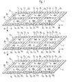
- Fig. 1 shows a perspective, schematic representation to illustrate the manufacturing method according to the invention. Shown are three foils 1, 2 and 3 made from a still unfired, piezoelectric ceramic material, ie from so-called green ceramic.
- a suitable material is e.g. B. lead barium titanate (PbBaTiO 2 ).
- the ceramic material can be z. B. by rolling, pouring or cutting into thin films.
- the order of magnitude of the film thickness is, for example, 0.1 mm, without the feasibility of the invention being restricted to this film thickness.
- the films 4 1 , 4 2 , 4 3 are coated with an electrically conductive material, preferably with a thin metal layer. All known chemical and physical surface coating processes, e.g. B.
- the electrodes 5 1 to 10 1 , 5 2 to 10 2 and 5 3 to 10 3 can be applied over the entire surface. In a screen printing process, however, a mesh-like structure of the electrodes is expedient.
- an electrode 5 1 to 10 1 , 5 2 to 10 2 or 5 3 to 10 3 of each film 1, 2 or 3 is assigned to an actuator.
- a plurality of actuators arranged laterally offset from one another are therefore processed simultaneously by the method according to the invention, as a result of which the production costs can be significantly reduced. In principle, it is also possible to assign not only one but several electrodes to each actuator if this is desirable for individual applications.
- the connection openings 11 to 22 serve to contact the individual electrodes 5 to 10, which will be discussed in more detail below.
- the second connection openings 17 1 to 22 1 are each surrounded by a recess 23 1 to 28 1 , ie the electrode coating does not extend to the edge of the second connection openings 17 1 to 22 1 , but the edge of the electrodes 5 1 to 10 1 is spaced from the edge of the second connection openings 17 1 to 22 1 .
- the electrodes 5 3 to 10 3 of the third film 3 have recesses 23 3 to 28 3 which surround the second connection openings 17 3 to 22 3 .
- the recesses 23 2 to 28 2 of the electrodes 5 2 to 10 2 surround the first connection openings 11 2 to 16 2 .
- cutouts 23 to 28 are therefore assigned alternately from film layer to film layer to the first connection openings 11 to 16 or the second connection openings 17 to 22, respectively.
- perforation holes 30 1 , 30 2 and 30 3 are provided in each film layer 1, 2 and 3 in the illustrated embodiment. B. can be formed by punching or drilling simultaneously with the first connection openings 11 to 16 and the second connection openings 17 to 22.
- the perforation holes 30 are network-like and in each case mark the boundary line between the individual actuators produced simultaneously using the method according to the invention.
- net-like intermediate regions 31 1 and 31 2 and 31 3 are provided in each film, so that the electrodes 5 to 10 do not reach extend outer edge of the actuators, but are spaced from the edge marked by the perforation holes 30.
- the perforation holes 30 are preferably arranged in rows in the intermediate regions 31, which extend along the edges of the individual actuators.
- actuators with a rectangular cross section are manufactured.
- the perforation holes must be arranged accordingly varied.
- a large number of films of which in Fig. 1 only sections of the films 1 to 3 are shown, stacked one above the other.
- the individual film layers are aligned with each other so that both the Perforation holes 30 as well as the first connection openings 11 to 16 and the second Connection openings 17 to 22 are positioned exactly one above the other. This can e.g. B. fully automatically with a mechanically or optically scanned reference marking system respectively.
- the stacking or layering of the individual foils 1 to 3 is shown in FIG. 1 illustrated by arrows 40 to 43.
- the layer sequence the films 1 to 3 selected so that the stacked connection openings 11 to 16 or 17 to 22 alternately only in every second film layer 1 to 3 of one Recess 23 to 28 of the electrodes 5 to 10 are surrounded, so that the electrodes 5 to 10 alternately with the first connection openings 11 to 16 or the second Connection openings 17 to 22 are connected.
- connection openings 11 to 16 and the second connection openings 17 to 22 with a suitable, electrically conductive Paste, e.g. B. a metallization paste filled.
- a suitable, electrically conductive Paste e.g. B. a metallization paste filled.
- Filling the connection openings 11 to 16 or 17 to 22 can e.g. B. by suction by means of vacuum or by Press in.
- the electrically conductive paste is preferably introduced into the already stacked condition of the foils. However, it is also conceivable that each one Foil is filled with the electrically conductive paste before stacking.
- the Connection openings 11 to 16 or 17 to 22 can also be called via holes are referred to, so that the contacting process is called the via-fill process due.
- the stacking of foils 1 to 3 resulting stacked arrangement under a suitable pressure at elevated temperature dried and then fired at a suitable temperature.
- the firing temperature is preferably greater than 1000 ° C and is preferably in the range between 1000 ° C and 1500 ° C.
- the fired, stacked arrangement is then broken down into the individual actuators.
- a film size of 15 x 20 cm can accommodate up to 200 individual actuators win the stacked arrangement.
- the separation into the individual actuators takes place, for. B. by sawing or by water jet cutting. Make the perforation holes 30 easier thereby the separation process and mark the separation point.
- the stacked ones are separated Arrangement in the individual actuators in that adjacent actuators with an electrical Voltage of different polarity can be applied. Because of that in the individual Layers of the actuator-forming electrical field, which between adjacent Actuators aligned in different directions result depending on the field direction either a contraction or expansion of the neighboring actuators. Between neighboring actuators therefore experience mechanical tension, which, if appropriate Dimensioning of the electric field strength and the distance between the individual Perforation holes 30 to separate the actuators along the Perforation holes 30 leads predetermined dividing line. This approach is special cost-saving, since no special separating device is required.
- a single actuator is shown in section in FIG. 2.
- the stacked layers 50 1 to 50 15 made of piezoelectric ceramic material can be seen.
- the electrodes 5 1 to 5 15 of the individual layers 50 1 to 50 15 can also be seen .
- the cutouts 23 1 to 23 15 of the electrodes 5 1 to 5 15 are arranged alternately so that they alternately surround the first connection opening 11 and the second connection opening 17.
- electrically conductive paste 53, the electrodes 5 1 , 5 3 , ... 5 15 are each every second layer with a z. B. connected by soldering, bonding, welding or the like to the actuator, the first connecting wire 51.
- the electrodes 5 2 , 5 4 ,... 5 14 lying in between are connected to a second connecting wire 52 via the electrically conductive paste 53 introduced into the second connection openings 17.
- the electrical field which forms in the actuator when an electrical voltage is applied between the connecting wires 51 and 52 is therefore oriented in the same direction in all piezoelectric layers 50 1 to 50 15 , so that the contraction or expansion of each individual piezoelectric layer 15 1 to 15 15 added constructively to an overall stroke of the piezoelectric actuator.
- the broken perforation holes 30 in the edge region of the actuator can also be seen from FIG. 2.
- An additional insulation measure is only to be provided for the top electrode 5 1 .
- the top of the actuator is preferably covered by a suitable electrically insulating casting compound. This potting compound can be applied evenly before the stacked arrangement is separated into the individual actuators. It is also conceivable to apply an electrically insulating covering film to the top as a final layer.
- the perforation holes 30 not only facilitate the separation of the stacked arrangement into individual actuators, but in particular also support the gas escape as drying channels during drying and firing of the stacked arrangement.
- the method according to the invention can be used to produce piezoelectric actuators which manage with an operating voltage of less than 150 V and generate a force of more than 1000 N with an actuation stroke of 50 ⁇ m .
- the stacked arrangement can be broken down into individual actuators with almost any cross-sectional area by water cutting. So z. B. round, triangular or star-shaped actuators can be produced.
Landscapes
- Engineering & Computer Science (AREA)
- Manufacturing & Machinery (AREA)
- Particle Formation And Scattering Control In Inkjet Printers (AREA)
- General Electrical Machinery Utilizing Piezoelectricity, Electrostriction Or Magnetostriction (AREA)
- Fuel-Injection Apparatus (AREA)
Abstract
Description
- Fig. 1
- eine schematische Darstellung von drei aufeinander zu stapelnden Folien aus einem piezoelektrischen Keramikmaterial, die mit Elektroden beschichtet sind und mit Verbindungsöffnungen und Perforationslöchern versehen sind; und
- Fig. 2
- einen fertigen Aktor in einer geschnittenen, perspektivischen Darstellung.
Claims (11)
- Verfahren zur parallelen Herstellung mehrerer piezoelektrischer Aktoren mit folgenden Verfahrensschritten:wobei die Verbindungsöffnungen (11-16, 17-22) die Folien (1-3) im Bereich der Elektroden (5-10) durchdringen und die Elektroden (5-10) jeweils eine Aussparung (23-28) aufweisen, die entweder die erste (11-16) oder zweite (17-22) Verbindungsöffnung umgibt,Herstellen von dünnen Folien (1-3) aus einem ungebrannten, piezoelektrischen Keramikwerkstoff,Ausbilden von die Folien (1-3) durchdringenden ersten und zweiten Verbindungsöffnungen (11-16, 17-22), wobei jedem Aktor jeweils eine erste (11-16) und eine zweite (17-22) Verbindungsöffnung zugeordnet ist,Beschichten jeweils einer Oberfläche (4) der Folien (1-3) mit mehreren Elektroden (5-10), wobei jedem Aktor in jeder Folie (1-3) zumindest eine Elektrode (5-10) zugeordnet ist undwobei die Schichtenfolge der Folien (1-3) so gewählt ist, dass die übereinander angeordneten Verbindungsöffnungen (11-16, 17-22) alternierend nur in jeder zweiten Folien-Schicht (1-3) von einer Aussparung (23-28) der Elektroden (5-10) umgeben sind, so dass die Elektroden (5-10) abwechselnd entweder mit den ersten Verbindungsöffnungen (11-16) oder den zweiten Verbindungsöffnungen (17-22) in Verbindung stehen,Stapeln einer Vielzahl von Folien (1-3) übereinander, so dass die ersten und zweiten Verbindungsöffnungen (11-16, 17-22) in einer dadurch entstehenden gestapelten Anordnung übereinander angeordnet sind,Einbringen einer elektrisch leitenden Paste (53) in die Verbindungsöffnungen (11-16, 17-22),Brennen der gestapelten Anordnung, undZertrennen der gestapelten Anordnung in einzelne Aktoren, dadurch gekennzeichnet, dass auf den Oberflächen (4) der Folien (1-3) im Randbereich zwischen den einzelnen Aktoren Zwischenbereiche (31) vorgesehen sind, die von den Elektroden (5-10) ausgespart sind, so dass das Zertrennen in einzelne Aktoren mit Abstand zu den jeweiligen Elektroden (5-10) erfolgt.
- Verfahren nach Anspruch 1,
dadurch gekennzeichnet, dass in den Zwischenbereichen (31) Perforationslöcher (30) ausgebildet werden. - Verfahren nach Anspruch 2,
dadurch gekennzeichnet, dass die Perforationslöcher (30) in sich in den Zwischenbereichen (31) entlang der Ränder der einzelnen Aktoren erstreckenden Reihen angeordnet sind. - Verfahren nach Anspruch 2 oder 3,
dadurch gekennzeichnet, dass zum Zertrennen der gestapelten Anordnung in die einzelnen Aktoren zwischen den Elektroden (5-10) benachbarter Aktoren ein elektrisches Feld entgegengesetzter Polarität angelegt wird. - Verfahren nach einem der Ansprüche 1 bis 4,
dadurch gekennzeichnet, dass das Zertrennen der gestapelten Anordnung in die einzelnen Aktoren mittels Sägen oder Wasserstrahlschneiden erfolgt. - Verfahren nach einem der Ansprüche 1 bis 5,
dadurch gekennzeichnet, dass die gestapelte Anordnung vor dem Brennen unter Druck bei einer erhöhten Temperatur getrocknet wird. - Verfahren nach einem der Ansprüche 1 bis 6,
dadurch gekennzeichnet, dass die Elektroden (5-10) durch ein Siebdruckverfahren, Aufdampfen, Sputtern oder dergleichen aufgebracht werden. - Verfahren nach einem der Ansprüche 1 bis 7,
dadurch gekennzeichnet, dass die gestapelte Anordnung beim Brennen unter uniaxialem Druck bei einer Temperatur von mindestens 1000 °C gesintert wird. - Piezoelektrischer Aktor, der eine Vielzahl von übereinander angeordneten Schichten (50) aus einem piezoelektrischen Keramikwerkstoff aufweist, die jeweils auf einer Oberfläche (4) mit zumindest einer Elektrode (5) beschichtet sind, wobei die Elektroden (5) alternierend miteinander verbunden sind und in jeder Schicht (50) eine erste und zweite die Schicht (50) im Bereich der Elektrode (5) durchdringende Verbindungsöffnung (11, 17) vorgesehen sind, wobei jede Elektrode (5) eine Aussparung (23) aufweist, die entweder die erste (11) oder zweite ( 17) Verbindungsöffnung umgibt, und die Schichten (50) so gestapelt sind, dass die ersten und zweiten Verbindungsöffnungen (11, 17) sämtlicher Schichten (50) übereinander angeordnet sind und die übereinander angeordneten Verbindungsöffnungen (11, 17) alternierend nur in jeder zweiten Schicht von einer Aussparung (23) der Elektroden (5) umgeben sind, so dass die Elektroden (5) abwechselnd mit den ersten Verbindungsöffnungen (11) und den zweiten Verbindungsöffnungen (17) in Verbindung stehen, und wobei die Verbindungsöffnungen (11, 17) mit einer elektrisch leitenden Paste (53) gefüllt sind,
dadurch gekennzeichnet, dass die Schichten (50) einen umlaufenden Randbereich (31) aufweisen, der nicht mit der Elektrode (5) beschichtet ist. - Piezoelektrischer Aktor nach Anspruch 9,
dadurch gekennzeichnet, dass die Elektroden (5) aus einer netzartigen Metallschicht bestehen. - Piezoelektrischer Aktor nach Anspruch 9 oder 10,
dadurch gekennzeichnet, dass die äußere Oberfläche der obersten und/oder untersten Schicht und/oder der Randbereich des Aktors in eine elektrisch isolierende Vergussmasse eingebettet ist.
Applications Claiming Priority (3)
| Application Number | Priority Date | Filing Date | Title |
|---|---|---|---|
| DE19757877 | 1997-12-24 | ||
| DE19757877A DE19757877A1 (de) | 1997-12-24 | 1997-12-24 | Verfahren zur Herstellung piezoelektrischer Aktoren und piezoelektrischer Aktor |
| PCT/DE1998/003174 WO1999034455A1 (de) | 1997-12-24 | 1998-10-30 | Verfahren zur herstellung piezoelektrischer aktoren und piezoelektrischer aktor |
Publications (2)
| Publication Number | Publication Date |
|---|---|
| EP1008193A1 EP1008193A1 (de) | 2000-06-14 |
| EP1008193B1 true EP1008193B1 (de) | 2004-10-06 |
Family
ID=7853389
Family Applications (1)
| Application Number | Title | Priority Date | Filing Date |
|---|---|---|---|
| EP98959777A Expired - Lifetime EP1008193B1 (de) | 1997-12-24 | 1998-10-30 | Verfahren zur herstellung piezoelektrischer aktoren und piezoelektrischer aktor |
Country Status (7)
| Country | Link |
|---|---|
| US (3) | US6263550B1 (de) |
| EP (1) | EP1008193B1 (de) |
| JP (1) | JP4440349B2 (de) |
| KR (1) | KR100655094B1 (de) |
| CZ (1) | CZ295943B6 (de) |
| DE (2) | DE19757877A1 (de) |
| WO (1) | WO1999034455A1 (de) |
Families Citing this family (28)
| Publication number | Priority date | Publication date | Assignee | Title |
|---|---|---|---|---|
| DE10024701A1 (de) * | 2000-05-18 | 2001-11-29 | Bosch Gmbh Robert | Piezoaktor |
| DE10041338A1 (de) * | 2000-08-23 | 2002-03-14 | Epcos Ag | Verfahren zum Herstellen eines keramischen Vielschichtbauelements sowie Grünkörper für ein keramisches Vielschichtbauelement |
| DE10126656A1 (de) * | 2001-06-01 | 2002-12-05 | Endress & Hauser Gmbh & Co Kg | Elektromechanischer Wandler mit mindestens einem piezoelektrischen Element |
| DE10147075A1 (de) * | 2001-09-25 | 2003-04-30 | Infineon Technologies Ag | Piezoelektrisches Bauelement und Verfahren zu dessen Herstellung |
| JP2003288158A (ja) * | 2002-01-28 | 2003-10-10 | Sony Corp | タクタイル・フィードバック機能を持つ携帯型機器 |
| GB2390479A (en) | 2002-06-06 | 2004-01-07 | Delphi Tech Inc | Poling method |
| JP2004356206A (ja) * | 2003-05-27 | 2004-12-16 | Fuji Photo Film Co Ltd | 積層構造体及びその製造方法 |
| JP4842520B2 (ja) * | 2003-05-30 | 2011-12-21 | 日本碍子株式会社 | セル駆動型圧電/電歪アクチュエータ及びその製造方法 |
| JP4438321B2 (ja) * | 2003-06-02 | 2010-03-24 | 株式会社デンソー | 積層型圧電体素子の製造方法 |
| DE10335019A1 (de) * | 2003-07-31 | 2005-02-17 | Robert Bosch Gmbh | Piezoaktor |
| US6941740B2 (en) * | 2003-10-15 | 2005-09-13 | Deere & Company | Baler gate linkage and latch structure |
| JP4261374B2 (ja) * | 2004-01-09 | 2009-04-30 | 富士フイルム株式会社 | 積層構造体及びその製造方法、並びに、超音波トランスデューサ |
| WO2005067070A1 (de) * | 2004-01-12 | 2005-07-21 | Siemens Aktiengesellschaft | Aktor mit innenliegender anschlusselektrode und herstellungsverfahren für einen solchen aktor |
| DE102004002087A1 (de) * | 2004-01-15 | 2005-08-04 | Robert Bosch Gmbh | Piezoaktor und ein Verfahren zu dessen Herstellung |
| JP4982031B2 (ja) * | 2004-01-16 | 2012-07-25 | 株式会社日立製作所 | コンテンツ送信装置、コンテンツ受信装置およびコンテンツ送信方法、コンテンツ受信方法 |
| JP2005340387A (ja) * | 2004-05-25 | 2005-12-08 | Tdk Corp | 積層型圧電素子及び燃料噴射装置 |
| FR2874663B1 (fr) * | 2004-08-31 | 2006-11-24 | Renault Sas | Dispositif de mise en vibration cyclique d'une buse d'injecteur |
| US7302744B1 (en) | 2005-02-18 | 2007-12-04 | The United States Of America Represented By The Secretary Of The Navy | Method of fabricating an acoustic transducer array |
| DE102005016798A1 (de) * | 2005-04-12 | 2006-10-19 | Robert Bosch Gmbh | Brennstoffeinspritzventil |
| JP5205689B2 (ja) * | 2005-08-25 | 2013-06-05 | Tdk株式会社 | 積層型圧電素子 |
| JP4752562B2 (ja) * | 2006-03-24 | 2011-08-17 | ヤマハ株式会社 | 鍵駆動装置及び鍵盤楽器 |
| DE102009028259A1 (de) * | 2009-08-05 | 2011-02-10 | Robert Bosch Gmbh | Verfahren zur Herstellung von piezoelektrischen Werkstücken |
| US8210661B2 (en) * | 2009-12-16 | 2012-07-03 | Palo Alto Research Center, Incorporated | Stacked slice printhead |
| DE102011003081A1 (de) | 2011-01-25 | 2012-07-26 | Robert Bosch Gmbh | Verfahren zur Herstellung von piezoelektrischen Werkstücken |
| DE102011003679A1 (de) | 2011-02-07 | 2012-08-09 | Robert Bosch Gmbh | Verfahren zur Herstellung von piezoelektrischen Werkstücken |
| DE102013100764B4 (de) * | 2013-01-25 | 2021-04-22 | Bürkert Werke GmbH | Verfahren zur Herstellung von durch physikalische Gasphasenabscheidung erzeugten Elektroden sowie ein Verfahren zur Herstellung von Piezoelementen mit durch physikalische Gasphasenabscheidung erzeugten Elektroden |
| CN111682103A (zh) * | 2020-05-29 | 2020-09-18 | 深圳振华富电子有限公司 | 一种带电极片式压电驱动器堆栈的制备方法 |
| JP2023043862A (ja) * | 2021-09-16 | 2023-03-29 | 方略電子股▲ふん▼有限公司 | 電子装置 |
Family Cites Families (15)
| Publication number | Priority date | Publication date | Assignee | Title |
|---|---|---|---|---|
| CH429228A (de) | 1964-12-10 | 1967-01-31 | Kistler Instrumente Ag | Piezoelektrischer Einbaukörper zum Einbau in einen piezoelektrischen Wandler |
| EP0094078B1 (de) * | 1982-05-11 | 1988-11-02 | Nec Corporation | Elektrostriktives Vielschichtelement welches wiederholter Pulsanwendung widersteht |
| JPS61205100A (ja) | 1985-03-08 | 1986-09-11 | Murata Mfg Co Ltd | 圧電発音体 |
| JPS62199075A (ja) | 1986-02-27 | 1987-09-02 | Fuji Elelctrochem Co Ltd | 積層型圧電素子の製造方法 |
| US4803393A (en) | 1986-07-31 | 1989-02-07 | Toyota Jidosha Kabushiki Kaisha | Piezoelectric actuator |
| DE3713697A1 (de) | 1987-04-24 | 1988-11-10 | Licentia Gmbh | Ultraschnelles steuerventil |
| US4967314A (en) * | 1988-03-28 | 1990-10-30 | Prime Computer Inc. | Circuit board construction |
| ES2087089T3 (es) | 1989-11-14 | 1996-07-16 | Battelle Memorial Institute | Metodo para fabricar un accionador piezoelectrico apilado multicapa. |
| JPH04299588A (ja) | 1991-03-28 | 1992-10-22 | Nec Corp | 電歪効果素子 |
| EP0651602B1 (de) * | 1993-10-29 | 1999-04-07 | Matsushita Electric Industrial Co., Ltd. | Leitfähige Pastenzusammensetzung zum Füllen von Kontaktlöchern, Leiterplatte unter Anwendung dieser leifähigen Paste und Verfahren zur Herstellung |
| US5519279A (en) | 1994-09-29 | 1996-05-21 | Motorola, Inc. | Piezoelectric resonator with grid-like electrodes |
| DE19500706C2 (de) | 1995-01-12 | 2003-09-25 | Bosch Gmbh Robert | Zumeßventil zur Dosierung von Flüssigkeiten oder Gasen |
| KR970705839A (ko) | 1995-06-27 | 1997-10-09 | 제이.쥐.에이.롤페즈 | 다층 전자 소자 제조 방법(Method of manufacturning multilayer electronic components) |
| JP2842382B2 (ja) | 1996-06-11 | 1999-01-06 | 日本電気株式会社 | 積層型圧電トランスおよびその製造方法 |
| TW432730B (en) | 1996-07-12 | 2001-05-01 | Taiheiyo Cement Corp | Piezoelectric transformer device |
-
1997
- 1997-12-24 DE DE19757877A patent/DE19757877A1/de not_active Ceased
-
1998
- 1998-10-30 JP JP53436999A patent/JP4440349B2/ja not_active Expired - Fee Related
- 1998-10-30 EP EP98959777A patent/EP1008193B1/de not_active Expired - Lifetime
- 1998-10-30 CZ CZ19992553A patent/CZ295943B6/cs not_active IP Right Cessation
- 1998-10-30 KR KR1019997007644A patent/KR100655094B1/ko not_active Expired - Fee Related
- 1998-10-30 WO PCT/DE1998/003174 patent/WO1999034455A1/de not_active Ceased
- 1998-10-30 US US09/380,019 patent/US6263550B1/en not_active Expired - Lifetime
- 1998-10-30 DE DE59812091T patent/DE59812091D1/de not_active Expired - Lifetime
-
2001
- 2001-04-18 US US09/837,127 patent/US20010022489A1/en not_active Abandoned
-
2002
- 2002-05-02 US US10/137,924 patent/US6757947B2/en not_active Expired - Lifetime
Also Published As
| Publication number | Publication date |
|---|---|
| CZ295943B6 (cs) | 2005-12-14 |
| US6757947B2 (en) | 2004-07-06 |
| JP2001513269A (ja) | 2001-08-28 |
| JP4440349B2 (ja) | 2010-03-24 |
| KR100655094B1 (ko) | 2006-12-08 |
| CZ255399A3 (cs) | 1999-11-17 |
| EP1008193A1 (de) | 2000-06-14 |
| US20020130595A1 (en) | 2002-09-19 |
| WO1999034455A1 (de) | 1999-07-08 |
| DE59812091D1 (de) | 2004-11-11 |
| US20010022489A1 (en) | 2001-09-20 |
| US6263550B1 (en) | 2001-07-24 |
| DE19757877A1 (de) | 1999-07-01 |
| KR20000075584A (ko) | 2000-12-15 |
Similar Documents
| Publication | Publication Date | Title |
|---|---|---|
| EP1008193B1 (de) | Verfahren zur herstellung piezoelektrischer aktoren und piezoelektrischer aktor | |
| DE68926166T2 (de) | Verfahren zur Herstellung einer piezoelektrischen Stapelantriebsvorrichtung | |
| EP1512183B1 (de) | Monolithischer vielschichtaktor aus einem piezokeramischen oder elektrostriktiven material sowie herstellungsverfahren und elektrische aussenkontaktierung | |
| EP2126995B1 (de) | Verfahren zur Herstellung eines piezokeramischen Vielschichtaktors | |
| EP1597780B1 (de) | Elektrisches vielschichtbauelement und schichtstapel | |
| EP1908131B1 (de) | Verfahren zum herstellen eines monolithischen piezoaktors mit teilstapeln, monolithischer piezoaktor mit teilstapeln und verwendung des piezoaktors | |
| DE19860001C2 (de) | Piezoelektrisches Bauelement, Verfahren zu dessen Herstellung und Verwendung eines derartigen Bauelements | |
| DE19945933C1 (de) | Piezoaktor mit isolationszonenfreier elektrischer Kontaktierung und Verfahren zu dessen Herstellung | |
| EP1235285B1 (de) | Verfahren zur Herstellung piezokeramischer Vielschichtaktoren | |
| EP2543085B1 (de) | Piezoelektrisches bauelement | |
| EP2122701B1 (de) | Vielschichtbauelement sowie verfahren zur herstellung eines vielschichtbauelements | |
| EP2054951B1 (de) | Piezoelektrisches bauelement | |
| DE102006011293A1 (de) | Piezoaktor und Verfahren zum Herstellen eines Piezoaktors | |
| EP3058600A1 (de) | Vielschichtbauelement und verfahren zur herstellung eines vielschichtbauelements | |
| EP2798679B1 (de) | Piezostack mit passivierung und verfahren zur passivierung eines piezostacks | |
| DE102013100764B4 (de) | Verfahren zur Herstellung von durch physikalische Gasphasenabscheidung erzeugten Elektroden sowie ein Verfahren zur Herstellung von Piezoelementen mit durch physikalische Gasphasenabscheidung erzeugten Elektroden | |
| DE10041338A1 (de) | Verfahren zum Herstellen eines keramischen Vielschichtbauelements sowie Grünkörper für ein keramisches Vielschichtbauelement | |
| DE102005002980B3 (de) | Monolithischer Vielschichtaktor und Verfahren zu seiner Herstellung | |
| DE102006001656A1 (de) | Piezoaktor und Verfahren zur Herstellung desselben | |
| DE102012110556B4 (de) | Vielschichtbauelement und Verfahren zu dessen Herstellung | |
| DE102005033463B3 (de) | Piezoaktor | |
| DD293689A5 (de) | Laminierte keramikanordnung und verfahren zur herstellung derselben | |
| EP3262698B1 (de) | Verfahren zur herstellung von vielschichtbauelementen und vielschichtbauelement, insbesondere piezoaktoren | |
| WO2005031885A1 (de) | Piezoelektrisches element | |
| DE102004030973A1 (de) | Piezoaktuator |
Legal Events
| Date | Code | Title | Description |
|---|---|---|---|
| PUAI | Public reference made under article 153(3) epc to a published international application that has entered the european phase |
Free format text: ORIGINAL CODE: 0009012 |
|
| 17P | Request for examination filed |
Effective date: 20000110 |
|
| AK | Designated contracting states |
Kind code of ref document: A1 Designated state(s): CH DE FR GB IT LI |
|
| 17Q | First examination report despatched |
Effective date: 20030508 |
|
| GRAP | Despatch of communication of intention to grant a patent |
Free format text: ORIGINAL CODE: EPIDOSNIGR1 |
|
| GRAS | Grant fee paid |
Free format text: ORIGINAL CODE: EPIDOSNIGR3 |
|
| GRAA | (expected) grant |
Free format text: ORIGINAL CODE: 0009210 |
|
| AK | Designated contracting states |
Kind code of ref document: B1 Designated state(s): CH DE FR GB IT LI |
|
| REG | Reference to a national code |
Ref country code: GB Ref legal event code: FG4D Free format text: NOT ENGLISH |
|
| REG | Reference to a national code |
Ref country code: CH Ref legal event code: EP |
|
| PG25 | Lapsed in a contracting state [announced via postgrant information from national office to epo] |
Ref country code: LI Free format text: LAPSE BECAUSE OF NON-PAYMENT OF DUE FEES Effective date: 20041031 Ref country code: CH Free format text: LAPSE BECAUSE OF NON-PAYMENT OF DUE FEES Effective date: 20041031 |
|
| REF | Corresponds to: |
Ref document number: 59812091 Country of ref document: DE Date of ref document: 20041111 Kind code of ref document: P |
|
| GBT | Gb: translation of ep patent filed (gb section 77(6)(a)/1977) |
Effective date: 20050125 |
|
| REG | Reference to a national code |
Ref country code: CH Ref legal event code: PL |
|
| ET | Fr: translation filed | ||
| PLBE | No opposition filed within time limit |
Free format text: ORIGINAL CODE: 0009261 |
|
| STAA | Information on the status of an ep patent application or granted ep patent |
Free format text: STATUS: NO OPPOSITION FILED WITHIN TIME LIMIT |
|
| 26N | No opposition filed |
Effective date: 20050707 |
|
| REG | Reference to a national code |
Ref country code: FR Ref legal event code: PLFP Year of fee payment: 18 |
|
| PGFP | Annual fee paid to national office [announced via postgrant information from national office to epo] |
Ref country code: IT Payment date: 20151026 Year of fee payment: 18 Ref country code: GB Payment date: 20151026 Year of fee payment: 18 |
|
| PGFP | Annual fee paid to national office [announced via postgrant information from national office to epo] |
Ref country code: FR Payment date: 20151026 Year of fee payment: 18 |
|
| GBPC | Gb: european patent ceased through non-payment of renewal fee |
Effective date: 20161030 |
|
| REG | Reference to a national code |
Ref country code: FR Ref legal event code: ST Effective date: 20170630 |
|
| PG25 | Lapsed in a contracting state [announced via postgrant information from national office to epo] |
Ref country code: GB Free format text: LAPSE BECAUSE OF NON-PAYMENT OF DUE FEES Effective date: 20161030 Ref country code: FR Free format text: LAPSE BECAUSE OF NON-PAYMENT OF DUE FEES Effective date: 20161102 |
|
| PG25 | Lapsed in a contracting state [announced via postgrant information from national office to epo] |
Ref country code: IT Free format text: LAPSE BECAUSE OF NON-PAYMENT OF DUE FEES Effective date: 20161030 |
|
| PGFP | Annual fee paid to national office [announced via postgrant information from national office to epo] |
Ref country code: DE Payment date: 20171206 Year of fee payment: 20 |
|
| REG | Reference to a national code |
Ref country code: DE Ref legal event code: R071 Ref document number: 59812091 Country of ref document: DE |