EP1009042A2 - Elektrolumineszente Vorrichtung mit Arylethylenderivate in der Ladungslöchertransportschicht - Google Patents
Elektrolumineszente Vorrichtung mit Arylethylenderivate in der Ladungslöchertransportschicht Download PDFInfo
- Publication number
- EP1009042A2 EP1009042A2 EP99203961A EP99203961A EP1009042A2 EP 1009042 A2 EP1009042 A2 EP 1009042A2 EP 99203961 A EP99203961 A EP 99203961A EP 99203961 A EP99203961 A EP 99203961A EP 1009042 A2 EP1009042 A2 EP 1009042A2
- Authority
- EP
- European Patent Office
- Prior art keywords
- transport layer
- carbon atoms
- hole transport
- layer
- heteroaryl
- Prior art date
- Legal status (The legal status is an assumption and is not a legal conclusion. Google has not performed a legal analysis and makes no representation as to the accuracy of the status listed.)
- Withdrawn
Links
Images
Classifications
-
- C—CHEMISTRY; METALLURGY
- C08—ORGANIC MACROMOLECULAR COMPOUNDS; THEIR PREPARATION OR CHEMICAL WORKING-UP; COMPOSITIONS BASED THEREON
- C08G—MACROMOLECULAR COMPOUNDS OBTAINED OTHERWISE THAN BY REACTIONS ONLY INVOLVING UNSATURATED CARBON-TO-CARBON BONDS
- C08G61/00—Macromolecular compounds obtained by reactions forming a carbon-to-carbon link in the main chain of the macromolecule
- C08G61/02—Macromolecular compounds containing only carbon atoms in the main chain of the macromolecule, e.g. polyxylylenes
-
- C—CHEMISTRY; METALLURGY
- C09—DYES; PAINTS; POLISHES; NATURAL RESINS; ADHESIVES; COMPOSITIONS NOT OTHERWISE PROVIDED FOR; APPLICATIONS OF MATERIALS NOT OTHERWISE PROVIDED FOR
- C09K—MATERIALS FOR MISCELLANEOUS APPLICATIONS, NOT PROVIDED FOR ELSEWHERE
- C09K11/00—Luminescent materials, e.g. electroluminescent or chemiluminescent
- C09K11/06—Luminescent materials, e.g. electroluminescent or chemiluminescent containing organic luminescent materials
-
- C—CHEMISTRY; METALLURGY
- C08—ORGANIC MACROMOLECULAR COMPOUNDS; THEIR PREPARATION OR CHEMICAL WORKING-UP; COMPOSITIONS BASED THEREON
- C08G—MACROMOLECULAR COMPOUNDS OBTAINED OTHERWISE THAN BY REACTIONS ONLY INVOLVING UNSATURATED CARBON-TO-CARBON BONDS
- C08G61/00—Macromolecular compounds obtained by reactions forming a carbon-to-carbon link in the main chain of the macromolecule
- C08G61/12—Macromolecular compounds containing atoms other than carbon in the main chain of the macromolecule
- C08G61/122—Macromolecular compounds containing atoms other than carbon in the main chain of the macromolecule derived from five- or six-membered heterocyclic compounds, other than imides
-
- H—ELECTRICITY
- H10—SEMICONDUCTOR DEVICES; ELECTRIC SOLID-STATE DEVICES NOT OTHERWISE PROVIDED FOR
- H10K—ORGANIC ELECTRIC SOLID-STATE DEVICES
- H10K50/00—Organic light-emitting devices
-
- H—ELECTRICITY
- H10—SEMICONDUCTOR DEVICES; ELECTRIC SOLID-STATE DEVICES NOT OTHERWISE PROVIDED FOR
- H10K—ORGANIC ELECTRIC SOLID-STATE DEVICES
- H10K50/00—Organic light-emitting devices
- H10K50/10—OLEDs or polymer light-emitting diodes [PLED]
- H10K50/11—OLEDs or polymer light-emitting diodes [PLED] characterised by the electroluminescent [EL] layers
-
- H—ELECTRICITY
- H10—SEMICONDUCTOR DEVICES; ELECTRIC SOLID-STATE DEVICES NOT OTHERWISE PROVIDED FOR
- H10K—ORGANIC ELECTRIC SOLID-STATE DEVICES
- H10K85/00—Organic materials used in the body or electrodes of devices covered by this subclass
- H10K85/60—Organic compounds having low molecular weight
- H10K85/615—Polycyclic condensed aromatic hydrocarbons, e.g. anthracene
- H10K85/626—Polycyclic condensed aromatic hydrocarbons, e.g. anthracene containing more than one polycyclic condensed aromatic rings, e.g. bis-anthracene
-
- H—ELECTRICITY
- H10—SEMICONDUCTOR DEVICES; ELECTRIC SOLID-STATE DEVICES NOT OTHERWISE PROVIDED FOR
- H10K—ORGANIC ELECTRIC SOLID-STATE DEVICES
- H10K85/00—Organic materials used in the body or electrodes of devices covered by this subclass
- H10K85/60—Organic compounds having low molecular weight
- H10K85/615—Polycyclic condensed aromatic hydrocarbons, e.g. anthracene
- H10K85/622—Polycyclic condensed aromatic hydrocarbons, e.g. anthracene containing four rings, e.g. pyrene
-
- H—ELECTRICITY
- H10—SEMICONDUCTOR DEVICES; ELECTRIC SOLID-STATE DEVICES NOT OTHERWISE PROVIDED FOR
- H10K—ORGANIC ELECTRIC SOLID-STATE DEVICES
- H10K85/00—Organic materials used in the body or electrodes of devices covered by this subclass
- H10K85/60—Organic compounds having low molecular weight
- H10K85/615—Polycyclic condensed aromatic hydrocarbons, e.g. anthracene
- H10K85/623—Polycyclic condensed aromatic hydrocarbons, e.g. anthracene containing five rings, e.g. pentacene
-
- H—ELECTRICITY
- H10—SEMICONDUCTOR DEVICES; ELECTRIC SOLID-STATE DEVICES NOT OTHERWISE PROVIDED FOR
- H10K—ORGANIC ELECTRIC SOLID-STATE DEVICES
- H10K85/00—Organic materials used in the body or electrodes of devices covered by this subclass
- H10K85/60—Organic compounds having low molecular weight
- H10K85/631—Amine compounds having at least two aryl rest on at least one amine-nitrogen atom, e.g. triphenylamine
-
- H—ELECTRICITY
- H10—SEMICONDUCTOR DEVICES; ELECTRIC SOLID-STATE DEVICES NOT OTHERWISE PROVIDED FOR
- H10K—ORGANIC ELECTRIC SOLID-STATE DEVICES
- H10K85/00—Organic materials used in the body or electrodes of devices covered by this subclass
- H10K85/60—Organic compounds having low molecular weight
- H10K85/649—Aromatic compounds comprising a hetero atom
- H10K85/657—Polycyclic condensed heteroaromatic hydrocarbons
Definitions
- the present invention relates to organic electroluminescent devices.
- Organic electroluminescent devices are a class of opto-electronic devices where light emission is produced in response to an electrical current through the device.
- EL the common acronym for electroluminescent
- OLED organic light emitting diode
- OLED organic light emitting diode
- the term EL and EL devices will include devices described as OLED.
- Organic EL devices generally have a layered structure with an organic luminescent medium sandwiched between an anode and a cathode.
- the organic luminescent medium usually refers to an organic light emitting material or a mixture thereof in the form of a thin amorphous or crystalline film.
- Representatives of earlier organic EL devices are disclosed in US-A-3,172,862; US-A-3,173,050; Dresner, "Double Injection Electroluminescence in Anthracene", RCA Review, Vol. 30, pp. 322-334, 1969; and US-A-3,710,167.
- the organic luminescent medium was formed of a conjugated organic host material and a conjugated organic activating agent having condensed benzene rings.
- Naphthalene, anthracene, phenanthrene, pyrene, benzopyrene, chrysene, picene, carbazole, fluorene, biphenyl, terpheyls, quarterphenyls, triphenylene oxide, dihalobiphenyl, trans-stilbene, and 1,4-diphenylbutadiene were offered as examples of organic host materials.
- Anthracene, tetracene, and pentacene were named as examples of activating agents.
- the organic luminescent medium was present as a single layer having a thickness much above 1 micrometer. The voltage required to drive the EL devices was as much as a few hundreds volts, thus the luminous efficiency of these EL devices was rather low.
- the organic luminescent medium in this bi-layer configuration comprises of two extremely thin layers of organic film ( ⁇ 1.0 micrometer in combined thickness) sandwiched between the anode and cathode.
- the layer adjacent to the anode termed the hole-transport layer, is specifically chosen to transport predominantly holes only in the EL device.
- the layer adjacent to the cathode is specifically chosen to transport predominantly electrons only in the EL device.
- the interface or junction between the hole-transport layer and the electron-transport layer is referred to as the electron-hole recombination zone where the electron and hole recombine to produce electroluminescence with the least interference from the electrodes.
- This recombination zone can be extended beyond the interface region to include portions of the hole-transport layer or the electron-transport layer or both.
- the extremely thin organic luminescent medium offers reduced electrical resistance, permitting higher current densities for a given voltage applied on the EL device. Since the EL intensity is directly proportional to the current density through the EL device, this thin bi-layer construction of the organic luminescent medium allows the EL device to be operated with a voltage as low as a few volts, in contrast to the earlier EL devices. Thus, the bi-layer organic EL device has achieved a high luminous efficiency in terms of EL output per electrical power input and is therefore useful for applications such as flat-panel displays and lighting.
- Commonly-assigned US-A-4,356,429 disclosed an EL device formed of an organic luminescent medium including a hole transport layer containing 1000 Angstroms of a porphyrinic compound such as copper phthalocyanine, and an electron transport layer of 1000 Angstroms of tetraphenylbutadiene in poly(styrene).
- the anode was formed of a conductive indium-tin-oxide (ITO) glass and the cathode was a layer of silver.
- the EL device emitted blue light when biased at 20 volts at an average current density in the 30 to 40 mA/cm 2 range. The brightness of the device was 5 cd/m 2 .
- aromatic amines as the material for the hole-transport layer in organic EL devices has since been generally recognized as numerous prior arts have disclosed the utility of various classes of amines in enhancing the EL device performance. Improvements in the hole-transport material parameters include higher hole transport mobility, more amorphous structures, higher glass transition temperature, and better electrochemical stability. Improvements in the organic EL devices with these improved amines include higher luminous efficiency, longer operational and storage life, and a greater thermal tolerance. For example, the improved arylamine hole transport materials have been disclosed in commonly-assigned US-A-5,061,569.
- An organic multilayer electroluminescent device including an anode and cathode, and comprising therebetween:
- the arylethylene and arylacetylene derivatives in accordance with the present invention have an ionization potential larger than 5.0 eV.
- the hole transport layer in accordance with the present invention effectively works with the electron transport layer or an emissive layer or an electron transport layer which also functions as an emissive layer to provide a highly efficient electroluminescent device.
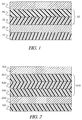
- FIG. 1 illustrates the basic structure used in the construction of organic EL device of this invention. It is a bi-layer structure comprising an organic hole transport layer 30 and an organic electron transport layer 40.
- the electron transport layer is also the emissive layer from which electroluminescence originates. Together, they form the organic EL medium 50.
- the anode 20 is adjacent to the hole transport layer and the cathode 60 is adjacent to the electrode transport layer.
- the substrate is layer 10. This figure is for illustration only and the individual layer thickness is not scaled according to the actual thickness.
- FIG. 2 illustrates an alternative construction of the organic EL device of this invention. It is a modified bi-layer structure.
- the EL medium contains an emissive layer between the hole transport layer and the electron transport layer. This emissive layer is the layer from which electroluminescence originates.
- layer 300 is the hole transport layer
- layer 400 is the emissive layer
- layer 500 is the electron transport layer
- the substrate is layer 100. This figure is for illustration only and the individual layer thickness is not scaled according to the actual thickness.
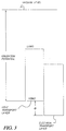
- FIG. 3 illustrates the energy level diagram of an organic EL device with a bi-layer structure as described in FIG. 1.
- the organic EL medium is represented by a hole-transport layer with a characteristic low ionization potential energy, and an electron transport layer with a relatively higher ionization potential energy.
- the ionization potential energy or ionization potential (IP) for a molecular solid is defined as the energy difference between the vacuum level and the highest occupied molecular orbital (HOMO) level of the solid.
- the vacuum level is usually referred to as the reference level from which the energy levels of the molecular solid are measured.
- the HOMO is the highest energy level filled with electron and in which the hole is free to move.
- the lowest unoccupied molecular orbital (LUMO) is the lowest energy level devoid of electron and in which free electron is free to move.
- the energy difference between HOMO and LUMO is the bandgap within which there are no available molecular orbital states.
- the IP value is a measure of the minimum energy required to remove an electron from the molecular solid and can be easily obtained experimentally by photoemission techniques which have been well described in the literature.
- the bi-layer structure as illustrated in FIG. 1 is designed to confine the electron hole recombination at the interface between the hole transport layer and the electron transport layer. This confinement is accomplished by establishing either an electron injection barrier or a hole injection barrier or both at the interface.
- the hole injection barrier it is the difference between the HOMO levels of the hole transport and electron transport layers, as indicated by the symbol, ⁇ , in FIG. 3. For large ⁇ values, > 0.5 eV, the hole migrating through the hole transport layer towards the interface will be unable to overcome the potential energy barrier and will thus be trapped at the hole transport layer side of the interface.
- the electron injection barrier is the difference between the LUMO levels and a large electron injection barrier for electron injection will localize the electron at the electron transport layer side of the interface. As a result of these charge localizations created by a proper choice of the hole transport and electron transport materials, the electron hole pair will tend to recombine at the interface producing electroluminescence which is characteristics of the interface.
- arylamines Conventional hole transport materials used in EL devices are mostly arylamines because their hole mobility is among the highest found in common organic materials. Materials with a high mobility are desirable for current-driven devices such as organic EL as the voltage require to operate the device will be low.
- the arylamines are also known to have the lowest ionization potentials among organic materials. Thus, for creating a hole injection barrier between the hole transport layer and the electron transport layer in a bi-layer EL device, arylamines are appropriate. Highly efficient EL devices have been produced using a variety of arylamines as the hole transport layer.
- a class of arylamines found particularly useful in organic EL devices is represented by formula V: wherein
- arylamines are particularly useful as the hole transport material in EL devices.
- arylamines are useful as hole transport materials in EL devices, they do have a number of deficiencies.
- the hole injection barrier formed between the arylamine hole transport layer and the electron transport layer will cause the holes to localize in the arylamines which will also result in a loss of electroluminescence. For these reasons, new hole transport materials are useful to further improve the EL device performance.
- the new hole transport materials in this invention include arylethylene and arylacetylene derivatives with a molecular structure containing at least 20 carbon atoms;
- a representative class of the hole transport materials includes:
- the ionization potentials of some of these aromatic hydrocarbon hole transport materials have been measured and their values are compared with the arylamine hole transport materials as follows. It is noted that the aromatic hydrocarbon hole transport materials generally have a higher ionization potential than the arylamines.
- a higher ionization potential for the hole transport material is more favorable for hole injection from the hole transport layer to the electron transport layer in a bi-layer EL device resulting in a lower hole injection barrier and consequently a higher EL luminous efficiency.
- a preferred range for the ionization potentials is 5.0 eV or higher.
- An alternative criteria is that it should be as high as the ionization potential of the electron transport material in the bi-layer EL device.
- the hole transport materials of this invention can be deposited by a number of methods.
- the preferred method is by vacuum vapor deposition as these aromatic hydrocarbons have good thermal stability and can be sublimed into thin film. Alternately, they can be dissolved in appropriate solvents and be cast into thin film. Other deposition methods such as printing by the inkjet method, thermal transfer, laser abrasion and sputtering are useful.
- the bi-layer EL device is the basic structure providing high luminous efficiencies and low-voltage operation.
- Alternative EL device structures have been demonstrated providing improved device performance.
- These alternative device structures include features in addition to the basic bi-layer structure such as the following structure (a) hole injection layer as disclosed in US-A-4,356,429; (b) cathode modification with alkaline or alkaline halides as disclosed in US-A-5,776,622; (c) anode modification with plasma-deposited flurocarbons, and (d) doped emitter layer inserted between the hole transport and electron transport layer as disclosed in US-A-4,769,292.
- These EL device structures retain the hole transport layer as one component of the electroluminescent medium. Therefore, the aromatic hydrocarbon or fused hydrocarbon hole transport materials disclosed in this invention are applicable to these EL device structures as well.
- a preferred EL device structure comprises an anode, a hole transport layer, an emissive layer, and an electron transport layer.
- the emissive layer is capable of transporting electrons as well, thus it can be considered as an electron transport layer with the added function of being highly luminescent.
- the principle function is to provide efficient emissive centers for electroluminescence.
- This emissive layer comprises a host material doped with one or more fluorescent dyes (FD).
- the fluorescent dye is usually present in an amount on the order of a few mole percent or less of the host material and it is sufficient to cause the EL emission to be predominantly that of the fluorescent dye. Using this method, highly efficient EL devices can be constructed.
- the color of the EL devices can be tuned by using fluorescent dyes of different emission wavelengths.
- fluorescent dyes of different emission wavelengths By using a mixture of fluorescent dyes, EL color characteristics of the combined spectra of the individual fluorescent dyes are produced. This dopant scheme has been described in considerable details for EL devices in commonly-assigned US-A-4,769,292.
- Preferred host materials for the emissive layer of the organic EL device disclosed in this invention are metal chelated oxinoid compounds, including chelates of oxine itself (also commonly referred to as 8-quinolinol or 8-hydroxyquinoline or Alq).
- Another class of preferred host materials is a mix ligand 8-quinolinolato aluminum chelates which have been disclosed in US-A-5,141,671.
- Another class of preferred host materials is distrylstibene derivatives as disclosed in US-A-5,366,811.
- Preferred fluorescent dyes used as the dopant in the emissive layer include coumarins, stilbenes, distrylstilbenes, derivatives of anthracene, tetracene, perylenes, rhodamines, and arylamines
- the molecular structures of the preferred fluorescent dyes for the emissive layer in the EL device are listed as follows:
- Preferred materials for use in forming the electron transporting layer of the organic EL device are metal chelated oxinoid compounds, including chelates of oxine itself (also commonly referred to as 8 ⁇ quinolinol or 8 ⁇ hydroxyquinoline).
- Representative compounds are 8-hydroquinoline of the group III metals such as Al, In, Mg; and of the group II metals such as Mg, Zn; and of the group I metal such as Li.
- Preferred materials for use in forming the cathode of the EL devices of this invention are Mg, Li, or alloys of these materials as disclosed in US-A-5,429,884; and commonly-assigned US-A-5,776,622.
- the organic EL medium has an anode, a hole transport layer, an emissive and electron transport layer, and a cathode.
- the substrate was glass.
- the above deposition sequence was completed in a single sequence without a vacuum break between the deposition of individual layers.
- the completed EL device was then sealed with a cover glass plate in a dry glove box for protection against ambient environment.
- a desiccant material was also include in the sealed package to improve the storage life of the EL device.
- the organic EL medium has an anode, a hole transport layer, an emissive layer, an electron-transport layer, and a cathode.
- the substrate was glass.
- the above deposition sequence was completed in a single sequence without a vacuum break between the deposition of individual layers.
- the completed EL device was then sealed with a cover glass plate in a dry glove box for protection against ambient environment.
- a desiccant material was also include in the sealed package to improve the storage life of the EL device.
Landscapes
- Chemical & Material Sciences (AREA)
- Physics & Mathematics (AREA)
- Engineering & Computer Science (AREA)
- Materials Engineering (AREA)
- Organic Chemistry (AREA)
- Spectroscopy & Molecular Physics (AREA)
- Optics & Photonics (AREA)
- Health & Medical Sciences (AREA)
- Chemical Kinetics & Catalysis (AREA)
- Medicinal Chemistry (AREA)
- Polymers & Plastics (AREA)
- Electroluminescent Light Sources (AREA)
Applications Claiming Priority (2)
| Application Number | Priority Date | Filing Date | Title |
|---|---|---|---|
| US20807198A | 1998-12-09 | 1998-12-09 | |
| US208071 | 1998-12-09 |
Publications (2)
| Publication Number | Publication Date |
|---|---|
| EP1009042A2 true EP1009042A2 (de) | 2000-06-14 |
| EP1009042A3 EP1009042A3 (de) | 2002-07-03 |
Family
ID=22773061
Family Applications (1)
| Application Number | Title | Priority Date | Filing Date |
|---|---|---|---|
| EP99203961A Withdrawn EP1009042A3 (de) | 1998-12-09 | 1999-11-25 | Elektrolumineszente Vorrichtung mit Arylethylenderivate in der Ladungslöchertransportschicht |
Country Status (3)
| Country | Link |
|---|---|
| EP (1) | EP1009042A3 (de) |
| JP (1) | JP2000182778A (de) |
| KR (1) | KR20000048006A (de) |
Cited By (6)
| Publication number | Priority date | Publication date | Assignee | Title |
|---|---|---|---|---|
| US7537842B2 (en) | 2001-02-20 | 2009-05-26 | Isis Innovation Limited | Asymmetric dendrimers |
| US7592074B2 (en) | 2001-02-20 | 2009-09-22 | Isis Innovation Limited | Metal-containing dendrimers |
| US7632576B2 (en) | 2001-02-20 | 2009-12-15 | Isis Innovation Limited | Aryl-aryl dendrimers |
| CN103450883A (zh) * | 2012-05-30 | 2013-12-18 | 京东方科技集团股份有限公司 | 有机电子材料 |
| CN104051630A (zh) * | 2013-03-11 | 2014-09-17 | 海洋王照明科技股份有限公司 | 有机电致发光器件及其制备方法 |
| US9738591B2 (en) | 2009-12-21 | 2017-08-22 | Ramiz Boulos | Antimicrobial compounds |
Families Citing this family (3)
| Publication number | Priority date | Publication date | Assignee | Title |
|---|---|---|---|---|
| US6420056B1 (en) * | 1999-07-08 | 2002-07-16 | International Business Machines Corporation | Electroluminescent device with dye-containing organic-inorganic hybrid materials as an emitting layer |
| KR100516137B1 (ko) * | 2002-08-06 | 2005-09-22 | 주식회사 이엘엠 | 청색발광재료9,10-비스[4-(2,2-디페닐비닐)페닐]안트라센(dpva)의유용한 전구체인1,1-디페닐-2-(4-디히드록시보론페닐)에텐(depb)의제조방법 |
| KR100464972B1 (ko) * | 2002-08-06 | 2005-01-06 | 주식회사 이엘엠 | 청색발광재료9,10-비스[4-(2,2-디페닐비닐)페닐]안트라센(dpva)의제조방법 |
Family Cites Families (1)
| Publication number | Priority date | Publication date | Assignee | Title |
|---|---|---|---|---|
| JP3642606B2 (ja) * | 1994-04-28 | 2005-04-27 | Tdk株式会社 | 有機el素子 |
-
1999
- 1999-11-25 EP EP99203961A patent/EP1009042A3/de not_active Withdrawn
- 1999-12-08 KR KR1019990055934A patent/KR20000048006A/ko not_active Withdrawn
- 1999-12-08 JP JP11348656A patent/JP2000182778A/ja active Pending
Cited By (13)
| Publication number | Priority date | Publication date | Assignee | Title |
|---|---|---|---|---|
| US8314549B2 (en) | 2001-02-20 | 2012-11-20 | Isis Innovation Limited | Metal-containing dendrimers |
| US7592074B2 (en) | 2001-02-20 | 2009-09-22 | Isis Innovation Limited | Metal-containing dendrimers |
| US7632576B2 (en) | 2001-02-20 | 2009-12-15 | Isis Innovation Limited | Aryl-aryl dendrimers |
| US7906902B2 (en) | 2001-02-20 | 2011-03-15 | Isis Innovation Limited | Metal-containing dendrimers |
| US7960725B2 (en) | 2001-02-20 | 2011-06-14 | Isis Innovation Limited | Aryl-aryl dendrimers |
| US7960557B2 (en) | 2001-02-20 | 2011-06-14 | Isis Innovation Limited | Asymmetric dendrimers |
| US7537842B2 (en) | 2001-02-20 | 2009-05-26 | Isis Innovation Limited | Asymmetric dendrimers |
| US8319213B2 (en) | 2001-02-20 | 2012-11-27 | Isis Innovation Limited | Aryl-aryl dendrimers |
| US9738591B2 (en) | 2009-12-21 | 2017-08-22 | Ramiz Boulos | Antimicrobial compounds |
| US10696620B2 (en) | 2009-12-21 | 2020-06-30 | Boulos & Cooper Pharmaceuticals Pty Ltd | Antimicrobial compounds |
| CN103450883A (zh) * | 2012-05-30 | 2013-12-18 | 京东方科技集团股份有限公司 | 有机电子材料 |
| CN103450883B (zh) * | 2012-05-30 | 2016-03-02 | 京东方科技集团股份有限公司 | 有机电子材料 |
| CN104051630A (zh) * | 2013-03-11 | 2014-09-17 | 海洋王照明科技股份有限公司 | 有机电致发光器件及其制备方法 |
Also Published As
| Publication number | Publication date |
|---|---|
| JP2000182778A (ja) | 2000-06-30 |
| KR20000048006A (ko) | 2000-07-25 |
| EP1009042A3 (de) | 2002-07-03 |
Similar Documents
| Publication | Publication Date | Title |
|---|---|---|
| EP1009044B1 (de) | Elektrolumineszente Vorrichtung mit Anthracenderivaten in der Löchertransportschicht | |
| US6361886B2 (en) | Electroluminescent device with improved hole transport layer | |
| US6699595B2 (en) | Electroluminescent device with polyphenyl hydrocarbon hole transport layer | |
| EP0825804B1 (de) | Blauorganische Elektrolumineszenzvorrichtungen | |
| US6475648B1 (en) | Organic electroluminescent devices with improved stability and efficiency | |
| EP1359790B1 (de) | Organische lichtemittierende Dioden mit verbesserter Betriebsstabilität | |
| EP1221473B1 (de) | Organische Leuchtdiodenvorrichtung mit emittierender Schicht aus drei Komponenten | |
| JP4116398B2 (ja) | 有機素子 | |
| US6696177B1 (en) | White organic electroluminescent devices with improved stability and efficiency | |
| US6603150B2 (en) | Organic light-emitting diode having an interface layer between the hole-transporting layer and the light-emitting layer | |
| JP4116399B2 (ja) | 有機発光素子 | |
| EP0903964A1 (de) | Organische elektrolumineszente Vorrichtung mit inorganischer ladungstransportierender Schicht | |
| JP2002043063A (ja) | 有機発光素子 | |
| KR20010080488A (ko) | 유기 전자발광 소자 및 유기 발광 매체 | |
| EP1009042A2 (de) | Elektrolumineszente Vorrichtung mit Arylethylenderivate in der Ladungslöchertransportschicht |
Legal Events
| Date | Code | Title | Description |
|---|---|---|---|
| PUAI | Public reference made under article 153(3) epc to a published international application that has entered the european phase |
Free format text: ORIGINAL CODE: 0009012 |
|
| AK | Designated contracting states |
Kind code of ref document: A2 Designated state(s): AT BE CH CY DE DK ES FI FR GB GR IE IT LI LU MC NL PT SE |
|
| AX | Request for extension of the european patent |
Free format text: AL;LT;LV;MK;RO;SI |
|
| RIC1 | Information provided on ipc code assigned before grant |
Free format text: 7H 01L 51/20 A, 7H 05B 33/14 B, 7C 09K 11/06 B |
|
| PUAL | Search report despatched |
Free format text: ORIGINAL CODE: 0009013 |
|
| STAA | Information on the status of an ep patent application or granted ep patent |
Free format text: STATUS: THE APPLICATION HAS BEEN WITHDRAWN |
|
| PUAF | Information related to the publication of a search report (a3 document) modified or deleted |
Free format text: ORIGINAL CODE: 0009199SEPU |
|
| AK | Designated contracting states |
Kind code of ref document: A3 Designated state(s): AT BE CH CY DE DK ES FI FR GB GR IE IT LI LU MC NL PT SE |
|
| AX | Request for extension of the european patent |
Free format text: AL;LT;LV;MK;RO;SI |
|
| 18W | Application withdrawn |
Withdrawal date: 20020531 |
|
| D17D | Deferred search report published (deleted) |