EP1010534A2 - Substrat pour former une plaque à buses ayant des orifices dimensionnés et positionnés avec précision et son procédé de fabrication - Google Patents
Substrat pour former une plaque à buses ayant des orifices dimensionnés et positionnés avec précision et son procédé de fabrication Download PDFInfo
- Publication number
- EP1010534A2 EP1010534A2 EP99204150A EP99204150A EP1010534A2 EP 1010534 A2 EP1010534 A2 EP 1010534A2 EP 99204150 A EP99204150 A EP 99204150A EP 99204150 A EP99204150 A EP 99204150A EP 1010534 A2 EP1010534 A2 EP 1010534A2
- Authority
- EP
- European Patent Office
- Prior art keywords
- film
- substrate
- nozzle plate
- mandrel
- photoresist
- Prior art date
- Legal status (The legal status is an assumption and is not a legal conclusion. Google has not performed a legal analysis and makes no representation as to the accuracy of the status listed.)
- Withdrawn
Links
- 238000004519 manufacturing process Methods 0.000 title claims abstract description 13
- 239000000758 substrate Substances 0.000 claims abstract description 64
- 239000000463 material Substances 0.000 claims abstract description 29
- 238000000034 method Methods 0.000 claims description 35
- 238000000151 deposition Methods 0.000 claims description 7
- 229920002120 photoresistant polymer Polymers 0.000 abstract description 70
- 229910052751 metal Inorganic materials 0.000 abstract description 28
- 239000002184 metal Substances 0.000 abstract description 28
- 238000009713 electroplating Methods 0.000 description 10
- HEMHJVSKTPXQMS-UHFFFAOYSA-M Sodium hydroxide Chemical compound [OH-].[Na+] HEMHJVSKTPXQMS-UHFFFAOYSA-M 0.000 description 9
- CSCPPACGZOOCGX-UHFFFAOYSA-N Acetone Chemical compound CC(C)=O CSCPPACGZOOCGX-UHFFFAOYSA-N 0.000 description 6
- PXHVJJICTQNCMI-UHFFFAOYSA-N Nickel Chemical compound [Ni] PXHVJJICTQNCMI-UHFFFAOYSA-N 0.000 description 6
- 238000005323 electroforming Methods 0.000 description 5
- 230000015572 biosynthetic process Effects 0.000 description 4
- 230000005684 electric field Effects 0.000 description 4
- 238000005530 etching Methods 0.000 description 4
- 229910052451 lead zirconate titanate Inorganic materials 0.000 description 4
- 238000006243 chemical reaction Methods 0.000 description 3
- 238000004070 electrodeposition Methods 0.000 description 3
- 239000011521 glass Substances 0.000 description 3
- 229910052759 nickel Inorganic materials 0.000 description 3
- 238000000059 patterning Methods 0.000 description 3
- 239000002904 solvent Substances 0.000 description 3
- VYZAMTAEIAYCRO-UHFFFAOYSA-N Chromium Chemical compound [Cr] VYZAMTAEIAYCRO-UHFFFAOYSA-N 0.000 description 2
- XUPKQAHNMWQFSF-UHFFFAOYSA-K [O-]C#N.[K+].[Fe+2].[O-]C#N.[O-]C#N Chemical compound [O-]C#N.[K+].[Fe+2].[O-]C#N.[O-]C#N XUPKQAHNMWQFSF-UHFFFAOYSA-K 0.000 description 2
- 229910052804 chromium Inorganic materials 0.000 description 2
- 239000011651 chromium Substances 0.000 description 2
- 239000004020 conductor Substances 0.000 description 2
- 230000003760 hair shine Effects 0.000 description 2
- HFGPZNIAWCZYJU-UHFFFAOYSA-N lead zirconate titanate Chemical compound [O-2].[O-2].[O-2].[O-2].[O-2].[Ti+4].[Zr+4].[Pb+2] HFGPZNIAWCZYJU-UHFFFAOYSA-N 0.000 description 2
- 239000012811 non-conductive material Substances 0.000 description 2
- 238000001020 plasma etching Methods 0.000 description 2
- 238000007747 plating Methods 0.000 description 2
- VYPSYNLAJGMNEJ-UHFFFAOYSA-N silicon dioxide Inorganic materials O=[Si]=O VYPSYNLAJGMNEJ-UHFFFAOYSA-N 0.000 description 2
- 206010034972 Photosensitivity reaction Diseases 0.000 description 1
- 239000000853 adhesive Substances 0.000 description 1
- 230000001070 adhesive effect Effects 0.000 description 1
- 238000010420 art technique Methods 0.000 description 1
- 229910002113 barium titanate Inorganic materials 0.000 description 1
- JRPBQTZRNDNNOP-UHFFFAOYSA-N barium titanate Chemical compound [Ba+2].[Ba+2].[O-][Ti]([O-])([O-])[O-] JRPBQTZRNDNNOP-UHFFFAOYSA-N 0.000 description 1
- 230000000903 blocking effect Effects 0.000 description 1
- 239000000919 ceramic Substances 0.000 description 1
- 238000003486 chemical etching Methods 0.000 description 1
- 238000004140 cleaning Methods 0.000 description 1
- 239000003989 dielectric material Substances 0.000 description 1
- NKZSPGSOXYXWQA-UHFFFAOYSA-N dioxido(oxo)titanium;lead(2+) Chemical compound [Pb+2].[O-][Ti]([O-])=O NKZSPGSOXYXWQA-UHFFFAOYSA-N 0.000 description 1
- 238000013467 fragmentation Methods 0.000 description 1
- 238000006062 fragmentation reaction Methods 0.000 description 1
- XLYOFNOQVPJJNP-UHFFFAOYSA-M hydroxide Chemical compound [OH-] XLYOFNOQVPJJNP-UHFFFAOYSA-M 0.000 description 1
- 238000007654 immersion Methods 0.000 description 1
- 150000002500 ions Chemical class 0.000 description 1
- UZUJHVIPEZFEKR-UHFFFAOYSA-L iron(2+);dicyanate Chemical compound [Fe+2].[O-]C#N.[O-]C#N UZUJHVIPEZFEKR-UHFFFAOYSA-L 0.000 description 1
- 230000001788 irregular Effects 0.000 description 1
- 238000000206 photolithography Methods 0.000 description 1
- 230000036211 photosensitivity Effects 0.000 description 1
- 239000010453 quartz Substances 0.000 description 1
- 229920005989 resin Polymers 0.000 description 1
- 239000011347 resin Substances 0.000 description 1
- 230000000284 resting effect Effects 0.000 description 1
- 229910052814 silicon oxide Inorganic materials 0.000 description 1
- 238000002207 thermal evaporation Methods 0.000 description 1
- 239000011032 tourmaline Substances 0.000 description 1
- 229940070527 tourmaline Drugs 0.000 description 1
- 229910052613 tourmaline Inorganic materials 0.000 description 1
Images





Classifications
-
- B—PERFORMING OPERATIONS; TRANSPORTING
- B41—PRINTING; LINING MACHINES; TYPEWRITERS; STAMPS
- B41J—TYPEWRITERS; SELECTIVE PRINTING MECHANISMS, i.e. MECHANISMS PRINTING OTHERWISE THAN FROM A FORME; CORRECTION OF TYPOGRAPHICAL ERRORS
- B41J2/00—Typewriters or selective printing mechanisms characterised by the printing or marking process for which they are designed
- B41J2/005—Typewriters or selective printing mechanisms characterised by the printing or marking process for which they are designed characterised by bringing liquid or particles selectively into contact with a printing material
- B41J2/01—Ink jet
- B41J2/135—Nozzles
- B41J2/16—Production of nozzles
- B41J2/162—Manufacturing of the nozzle plates
-
- B—PERFORMING OPERATIONS; TRANSPORTING
- B41—PRINTING; LINING MACHINES; TYPEWRITERS; STAMPS
- B41J—TYPEWRITERS; SELECTIVE PRINTING MECHANISMS, i.e. MECHANISMS PRINTING OTHERWISE THAN FROM A FORME; CORRECTION OF TYPOGRAPHICAL ERRORS
- B41J2/00—Typewriters or selective printing mechanisms characterised by the printing or marking process for which they are designed
- B41J2/005—Typewriters or selective printing mechanisms characterised by the printing or marking process for which they are designed characterised by bringing liquid or particles selectively into contact with a printing material
- B41J2/01—Ink jet
- B41J2/135—Nozzles
- B41J2/16—Production of nozzles
- B41J2/1621—Manufacturing processes
- B41J2/1625—Manufacturing processes electroforming
-
- B—PERFORMING OPERATIONS; TRANSPORTING
- B41—PRINTING; LINING MACHINES; TYPEWRITERS; STAMPS
- B41J—TYPEWRITERS; SELECTIVE PRINTING MECHANISMS, i.e. MECHANISMS PRINTING OTHERWISE THAN FROM A FORME; CORRECTION OF TYPOGRAPHICAL ERRORS
- B41J2/00—Typewriters or selective printing mechanisms characterised by the printing or marking process for which they are designed
- B41J2/005—Typewriters or selective printing mechanisms characterised by the printing or marking process for which they are designed characterised by bringing liquid or particles selectively into contact with a printing material
- B41J2/01—Ink jet
- B41J2/135—Nozzles
- B41J2/16—Production of nozzles
- B41J2/1621—Manufacturing processes
- B41J2/1626—Manufacturing processes etching
- B41J2/1628—Manufacturing processes etching dry etching
-
- B—PERFORMING OPERATIONS; TRANSPORTING
- B41—PRINTING; LINING MACHINES; TYPEWRITERS; STAMPS
- B41J—TYPEWRITERS; SELECTIVE PRINTING MECHANISMS, i.e. MECHANISMS PRINTING OTHERWISE THAN FROM A FORME; CORRECTION OF TYPOGRAPHICAL ERRORS
- B41J2/00—Typewriters or selective printing mechanisms characterised by the printing or marking process for which they are designed
- B41J2/005—Typewriters or selective printing mechanisms characterised by the printing or marking process for which they are designed characterised by bringing liquid or particles selectively into contact with a printing material
- B41J2/01—Ink jet
- B41J2/135—Nozzles
- B41J2/16—Production of nozzles
- B41J2/1621—Manufacturing processes
- B41J2/1626—Manufacturing processes etching
- B41J2/1629—Manufacturing processes etching wet etching
-
- B—PERFORMING OPERATIONS; TRANSPORTING
- B41—PRINTING; LINING MACHINES; TYPEWRITERS; STAMPS
- B41J—TYPEWRITERS; SELECTIVE PRINTING MECHANISMS, i.e. MECHANISMS PRINTING OTHERWISE THAN FROM A FORME; CORRECTION OF TYPOGRAPHICAL ERRORS
- B41J2/00—Typewriters or selective printing mechanisms characterised by the printing or marking process for which they are designed
- B41J2/005—Typewriters or selective printing mechanisms characterised by the printing or marking process for which they are designed characterised by bringing liquid or particles selectively into contact with a printing material
- B41J2/01—Ink jet
- B41J2/135—Nozzles
- B41J2/16—Production of nozzles
- B41J2/1621—Manufacturing processes
- B41J2/1631—Manufacturing processes photolithography
-
- B—PERFORMING OPERATIONS; TRANSPORTING
- B41—PRINTING; LINING MACHINES; TYPEWRITERS; STAMPS
- B41J—TYPEWRITERS; SELECTIVE PRINTING MECHANISMS, i.e. MECHANISMS PRINTING OTHERWISE THAN FROM A FORME; CORRECTION OF TYPOGRAPHICAL ERRORS
- B41J2/00—Typewriters or selective printing mechanisms characterised by the printing or marking process for which they are designed
- B41J2/005—Typewriters or selective printing mechanisms characterised by the printing or marking process for which they are designed characterised by bringing liquid or particles selectively into contact with a printing material
- B41J2/01—Ink jet
- B41J2/135—Nozzles
- B41J2/16—Production of nozzles
- B41J2/1621—Manufacturing processes
- B41J2/164—Manufacturing processes thin film formation
- B41J2/1643—Manufacturing processes thin film formation thin film formation by plating
-
- C—CHEMISTRY; METALLURGY
- C25—ELECTROLYTIC OR ELECTROPHORETIC PROCESSES; APPARATUS THEREFOR
- C25D—PROCESSES FOR THE ELECTROLYTIC OR ELECTROPHORETIC PRODUCTION OF COATINGS; ELECTROFORMING; APPARATUS THEREFOR
- C25D1/00—Electroforming
- C25D1/08—Perforated or foraminous objects, e.g. sieves
Definitions
- This invention generally relates to print head nozzle plates and methods and more particularly relates to a mandrel for forming an ink jet nozzle plate having orifices of precise size and location, and method of making the mandrel.
- An ink jet printer produces images on a receiver by ejecting ink droplets onto the receiver in an imagewise fashion.
- the advantages of non-impact, low-noise, low energy use, and low cost operation in addition to the capability of the printer to print on plain paper are largely responsible for the wide acceptance of ink jet printers in the marketplace.
- a print head formed of piezoelectric material includes a plurality of ink channels, each channel containing ink therein. Each of these channels is defined by a pair of oppositely disposed sidewalls. Also, each of these channels terminates in a channel opening for exit of ink droplets onto a receiver disposed opposite the openings.
- the piezoelectric material possesses piezoelectric properties such that an electric field applied to a selected pair of sidewalls produces a mechanical stress in the sidewalls. Thus, the pair of sidewalls inwardly deform as the mechanical stress is produced by the applied electric field. As the pair of sidewalls defining the channel inwardly deform, an ink droplet is squeezed from the channel.
- piezoelectric ceramics Some naturally occurring materials possessing such piezoelectric characteristics are quartz and tourmaline.
- the most commonly produced piezoelectric ceramics are lead zirconate titanate (PZT), barium titanate, lead titanate, and lead metaniobate.
- PZT lead zirconate titanate
- barium titanate barium titanate
- lead titanate lead metaniobate.
- a nozzle plate to the print head such that the nozzle plate faces the receiver, so that the ink droplet achieves the desired volume and trajectory.
- the nozzle plate has nozzle orifices therethrough aligned with respective ones of the channel openings.
- the purpose of the orifices is to produce ink droplets having a predetermined volume and velocity.
- Another purpose of the orifices is to direct each ink droplet along a trajectory normal (i.e., at a right angle) to the nozzle plate and thus normal to the receiver surface. If diameter of the nozzle orifice deviates from a desired diameter, ink droplet trajectory, volume and velocity can vary from desired values.
- each orifice is preferably precisely dimensioned so that each ink droplet exiting any of orifices travels along the predetermined trajectory with predetermined volume and velocity. This is important in order to avoid image artifacts, such as banding. Therefore, the technique used to make the nozzle plate should produce nozzle plate orifices that are precisely dimensioned and located to avoid such undesirable image artifacts.
- Such a nozzle plate may be formed by a "negative relief" electroplating patterning process.
- a mandrel is formed by overcoating a substrate (e.g., silicon oxide or other nonconductive material) with a conductive film (e.g., chromium or nickel).
- a photoresist layer is then applied to the conductive film, which photoresist layer may be formed of sensitized resins or other suitable material.
- the photoresist layer is imaged and developed to expose selected areas of the conductive film. These selected exposed areas of conductive film are removed by exposing the film to an etchant, thereby leaving a relief pattern to complete formation of the previously mentioned mandrel.
- an etchant may be sodium hydroxide and potassium iron cyanate.
- the selected areas removed from the conductive film are circular holes, each hole corresponding to one of the nozzle orifices.
- the nozzle plate itself may be formed by using the mandrel in combination with an electroplating process.
- a layer of metal is electroplated over the conductive film and initially covers only the conductive film. Thereafter, the metal layer develops a growth front that closes over the circular holes where the conductive film was removed.
- the orifice diameter is defined by the edge of the growth front of the metal layer on the substrate.
- nozzle orifice diameter is determined by controlling the electroplating time.
- nozzle plates may be formed by an electroforming process using a mandrel having a "positive relief" pattern, such as caused by nonconductive disks on the conductive surface of the substrate, rather than the "negative relief” pattern mentioned hereinabove.
- a problem associated with each of these processes is variability of diameter of nozzle orifices. This may be due to the growth rate of the metal layer varying at different areas of the mandrel in the electroplating process (or electroforming process). Such variability in growth rate of the metal layer results in variability in diameter of the orifices, which diameter is defined by the previously mentioned growth front of the metal layer. Even relatively slight variability in growth rate of the metal layer in the electroplating (or electroforming) process can result in large relative error in orifice diameter. This problem is particularly severe when the techniques hereinabove are used to produce nozzle plates having small diameters which may be on the order of 10 ⁇ m to 30 ⁇ m. Thus, a problem in the art is variability in orifice diameter during manufacture of the nozzle plate.
- Still another problem in the art is variability in nozzle orifice shape. That is, the prior art techniques mentioned hereinabove may sometimes produce noncircular orifices. This is undesirable because variability in orifice shape may also produce the previously mentioned image artifacts, such as banding. Such variability in orifice shape also may be due to uneven advancement of the metal layer growth front.
- an object of the present invention is to provide a mandrel for forming an ink jet nozzle plate having orifices of precise size and location, and method of making the mandrel.
- the invention resides in a method of making a nozzle plate, comprising the steps of providing a substrate; depositing a film on the substrate; forming a well extending through the film and into the substrate, the well having an upright column of predetermined width integrally attached to the substrate; and depositing a nozzle plate material on the film and into the well until a layer of the material defines an orifice having a width defined by the width of the column.
- a nozzle plate mandrel is formed by overcoating a substrate with a metal film.
- the film is covered with a photoresist material. Selected circular portions of the photoresist are exposed to light passing through a photomask having annular light-transparent regions, of precise diameters and pitch.
- the photoresist is subjected to a developer bath which dissolves the photoresist exposed to the light, thereby revealing selected portion of the film.
- an etchant is brought into contact with the film for etching-away portions of the film not covered by photoresist material. This etching process provides an annular opening in the film defining a region of precise diameter at the center of each opening.
- a second etching step is performed to create an annular recess extending into the substrate.
- the column resides at the center of the recess.
- a new photoresist layer is ten applied to the film. Selected portions of the new photoresist layer are exposed to light passing trough a second photomask.
- the second photomask is aligned to the annular features on the substrate, such that circular regions are exposed directly over the columns in the substrate.
- the new photoresist material is then subjected to the developer which dissolves the new photoresist material to reveal portions of the film beneath the photoresist and selected areas of the substrate, specifically the metal film-covered columns. Following this step, the substrate is again placed in an etchant to remove the exposed portions of the metal film.
- a metal layer that will form the nozzle plate is deposited onto the film and grows into the recess to substantially fill the recess, except for the space occupied by the column.
- the finished nozzle plate is separated from the film/substrate structure.
- the nozzle plate has orifices with precise diameters and pitch.
- An advantage of the present invention is that the mandrel is reusable.
- Another advantage of the present invention is that manufacturing errors are reduced.
- Yet another advantage of the present invention is that use thereof avoids missing (i.e., closed) nozzle orifices.
- a print head portion 10 for printing an image (not shown) on a receiver 20, which may be a reflective-type receiver (e.g., paper) or a transmissive-type receiver (e.g., transparency).
- Print head portion 10 has a surface 15 thereon.
- Formed in print head portion 10 are a plurality of spaced-apart parallel ink channels 30 (only five of which are shown), each channel 30 being defined by oppositely disposed sidewalls 40a and 40b.
- Each channel terminates in a channel outlet 50 opening onto surface 15, channel outlet 50 preferably being of generally circular shape.
- Attached to surface 15, such as by a suitable adhesive, and extending along surface 15 is a nozzle plate, generally referred to as 60.
- Nozzle plate 60 includes a plurality of nozzle orifices 70 therethrough centrally aligned with respective ones of channel outlets 50. According to the invention, each orifice 70 obtains a precisely dimensioned diameter D1 and all orifices 70 are arranged to obtain a precise constant pitch D2.
- the terminology "pitch" is defined herein to mean the center-to-center distance between adjacent orifices 70.
- each orifice 70 has a funnel-shaped discharge throat 75 diverging almost immediately from a rear side of nozzle plate 60 toward a front side of nozzle plate 60. It is important that each orifice 70 has a funnel-shaped discharge throat 75. This is important because such a divergent funnel shape advantageously provides a sharp "pinch point" for droplet 80 so that droplet 80 accurately and consistently forms when droplet 80 is discharged through throat 75.
- print head portion 10 is formed of a piezoelectric material, such as lead zirconate titanate (PZT).
- the piezoelectric material possesses piezoelectric properties so that an electric field (not shown) applied to a selected pair of sidewalls 40a/b produces a mechanical stress in the material.
- This pair of sidewalls 40a/b inwardly deform as the mechanical stress is produced by the applied electric field.
- an ink droplet 80 is squeezed from the channel by way of orifice 70.
- it is desirable tat ink droplet 80 exiting orifice 70 travel in a predetermined intended trajectory 90, so that droplet 80 lands on receiver 20 at a predetermined location.
- nozzle plate 60 is provided to ensure that droplet 80 exiting orifice 70 will travel along predetermined trajectory 90 rather than along an unintended trajectory 100. Also, nozzle plate 60 ensures that droplet 80 obtains a predetermined volume so that droplet 80 produces a pixel of predetermined size and also ensures that droplet 80 obtains a predetermined velocity. It has been found that orifice diameter D1 affect droplet trajectory, volume and velocity. As described in detail hereinbelow, nozzle plate 60 is fabricated by means of a mandrel produced by a photolithography process, such that nozzle plate 60 has orifices 70 of precise diameter D1 and pitch D2.
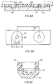
- a conductive film 110 (e.g., chromium, nickel, or other material suitable for plating and patterning) is deposited onto a nonconductive substrate 120 (e.g., glass or other dielectric material) in a continuous layer of uniform thickness.
- thickness of film 110 may be approximately 1000 ⁇ (angstroms) or more.
- Conductive film 110 has a top face 115.
- a light-sensitive photoresist layer 130 is deposited over the top of film 110 in a continuous layer of uniform thickness.
- thickness of photoresist layer 130 is not critical, it is nonetheless desirable that photoresist layer 130 have a uniform thickness. This uniform thickness should not vary from mandrel to mandrel that is manufactured.
- photoresist layer 130 may be approximately 0.5 to 2.0 microns thick.
- a first photomask (not shown) is disposed above photoresist layer 130.
- the photomask has a plurality of light-transparent annular regions, the regions having a predetermined diameter D1 and pitch D2. Of course, other areas of the photomask not including these regions having diameters D1 are opaque to light.
- a light source is disposed above the photomask and directs light through the transparent annular regions formed in the photomask. However, no light shines through a centermost circular portion of each region because the centermost portion is opaque. This centermost portion of the first photomask has diameter D1. As the light passes through each transparent annular region of the photomask, the light causes a chemical reaction in photoresist layer 130.
- a developer bath is preferably used to dissolve the areas of photoresist layer 130 that underwent the chemical reaction.
- a developer suitable for this purpose is tetrametylammonium hydroxide (TMAH).
- TMAH tetrametylammonium hydroxide
- This step in the process creates a "patterned" photoresist layer 155.
- Film 110, substrate 120, and patterned photoresist layer 155 now define a sandwiched structure, generally referred to as 170.
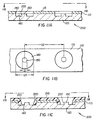
- an etchant is used to etch an annular trough 160 in film 110. It may appreciated that this etchant may be a wet or dry etchant. Sandwiched structure 170 is preferably placed in a bath containing etchant, which chemically reacts with exposed portions of film 110 and does not react with substrate 120 or patterned photoresist layer 155. Etchant suitable for this purpose is sodium hydroxide and potassium iron cyanate. Next, substrate 120 is anisotropically etched to reveal an annular recess 180.
- sandwiched structure 170 is preferably placed in a reactive ion etch chamber (not shown) to etch a predetermined depth "H" anisotropically into substrate 120, measured from the top face 115.
- Depth H is controlled such that depth H is uniform across surface of each recess 180 so that nozzle plate 60 will be appropriately formed. It may be appreciated with reference to the several figures that depth H is less than height of the film/substrate combination. By way of example only, and not by way of limitation, depth H may be approximately 1 to approximately 3 microns. Also, it may be appreciated from the teachings herein that patterned photoresist layer 155 and film 110 serve as a mask for etching substrate 120.
- patterned photoresist layer 155 is removed, such as by immersion in a solvent such as acetone, or by means of a plasma ash. This step in the process reveals film 110, including that portion of film 110 resting atop column 150.
- a new photoresist layer 130 is then applied to film 110.
- the new photoresist layer 130 is exposed to light passing through a light-transparent circular portion of a second photomask (not shown).
- the light exposes and chemically reacts with a preselected portion of the photoresist material.
- the photoresist material is then subjected to the developer which dissolves the exposed portion of the photoresist material.
- a circular well 190 is formed.
- Well 190 extends from a top surface 195 of photoresist layer 130 to recess 180 in substrate 120 and surrounds column 150.
- circular well 190 has a diameter D4 greater than diameter D1 but less than diameter D3.
- the second photomask must be aligned relative to substrate 120 to create by exposure and development opening 190 which coincides with column 150, but which does not coincide with diameter D3 of circular well 180.
- film 110 that resides atop column 150 is removed by means of chemical etching.
- An etchant suitable for this purpose is sodium hydroxide and iron cyanate. It may be appreciated that film 110 on column 150 is removed in this manner to prevent the electroplated layer from growing over column 150 when it contacts the edge of column 50.
- Photoresist layer 130 is then removed by application of a solvent such as acetone. Completion of this step in the process obtains a mandrel, generally referred to as 200, upon which nozzle plate 60 is formed, as described in detail presently.
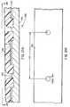
- nozzle plate 60 if formed by gradual electrodeposition of a metal layer 210 on top face 115 of film 110.
- metal layer 210 is nickel.
- Metal layer 210 first covers top face 115.
- a growth front 220 forms and metal layer 210 grows over sidewalls of well 190, eventually forming a funnel shape in transverse cross section and converging toward a vertical side-flank 222 of column 150.
- This electrodeposition step is terminated when growth front 220 comes into contact with side-flank 222.
- nozzle plate 70 has a thickness "T".
- column 150 stops growth front 220 from converging any further once growth front 220 contacts side-flank 222 allows the electrodeposition step to be carried-out for a slightly longer time than that of the prior art, without any of the resulting nozzle diameters D1 being smaller than desired.
- diameter D1 is precisely and consistently formed for each nozzle orifice 70 belonging to each individual nozzle plate 60 made by means of mandrel 200.
- discharge throat 75 advantageously provides a sharp "pinch point" for droplet 80 so that droplet 80 accurately and consistently forms when droplet 80 is discharged through throat 75.
- nozzle plate 60 is separated from mandrel 200, such as by releasing (i.e., lifting or separating) nozzle plate 60 in direction of arrows 225.
- all orifices 70 now have precise diameters D1 and pitch D2.
- diameter D1 may be 20 microns and nozzle plate 60 may be 25 microns thick, for example.
- column 150 Without column 150, a 5% deviation in the growth rate of front 220 would result in a 3 micron deviation in nozzle diameter D1 from nozzle orifice to nozzle orifice of the same nozzle plate or among a plurality of nozzle plates. This 3 micron deviation would represent a 15% error in nozzle orifice diameter.
- column 150 defines the nozzle orifice diameter. In this manner, nozzle orifice diameter D1 can be easily controlled to within 1 micron. Thus, column 150 only needs to block growth variability of 1.5 microns from the wall of well 190. By way of example only, and not by way of limitation, a 2 micron height for column 150 is sufficient for blocking growth front 220.
- diameter D3 of recess 180 is a function of diameter D1, depth H and thickness of the nozzle plate 60 as follows: D3 ⁇ D1 + 2T + H where,
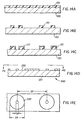
- mandrel 200 is made by a "lift-off" process, rather than by the etching process described hereinabove. That is, positive photoresist layer 130 is deposited on substrate 120. Positive photoresist layer 130 is then exposed to light passing through the previously mentioned photomask. Next, with the photomask removed, photoresist layer 130 is subjected to an "image reversal" treatment, which renders all previously exposed photoresist insoluble to developer while all unexposed photoresist retains its photosensitivity.
- photoresist layer 130 is "flood exposed" to the light source.
- Photoresist layer 130 is then developed by means of a suitable developer (e.g., TMAH). The developer dissolves-away only areas which were not initially exposed to light through the photomask.
- TMAH e.g., TMAH
- the pattern produced on glass substrate 120 results in an annular photoresist region 230 having desired inner diameter D1 and outer diameter D3.
- diameter D1 defines an area centrally located within annular region 230 where photoresist has been removed.
- a metal film 110 is then deposited, such as by thermal evaporation, on the substrate 120 and photoresist layer 130.
- the photoresist layer 130 and the portions of metal film 110, which cover the photoresist, are then removed, such as by application of a solvent (e.g., acetone).
- a solvent e.g., acetone
- This step exposes areas of glass substrate 10 such that annular region 230 of substrate 10 has well-defined sharp-edged boundaries.
- the processes forward to complete creation of the mandrel and the electroformed nozzle plate are identical to those previously described with the exception that in this embodiment, only metal film 110 provides the mask during the reactive ion etching into substrate 120. In other words, no photoresist remains in substrate 10 at the point when the reactive ion etching is taking place.
- mandrel 200 is reusable. This is so because recess 180 is permanently etched into substrate 120 and conductive film 110 remains on substrate 120. Therefore, no further processing is necessary to reuse mandrel 200 in order to produce more nozzle plates 60, with the exception of a cleaning step prior to reuse.
- Another advantage of the present invention is that manufacturing errors are reduced. This is so because the process of the invention uses photolithographically-defined column 150 which allows a more precise control of growth front 220 compared to prior art electroplating processes, which rely solely on control of the electroplating time and conditions. Use of the photolithographically-defined column 150 allows relaxation of control over the plating process for making nozzle orifices 70 having uniform diameters D1.
- Still another advantage of the present invention is that only a single photomask need be used rather than a plurality of photomasks to define the annular areas 140 and columns 150. That is, diameter D1 and diameter D3 are formed with use of single photomask, eliminating need to align column 150 within annular areas 140. Not only does this save time in the mandrel fabrication step; it also insures that column 150 will be centered within annular areas 140. Especially in the case of fabricating small diameter nozzles orifices 70, a misregistration of column 150 within annular area 140 of even 1 micron will produce non-symmetrical nozzles.
- the second photomask used in the process of the invention serves only to uncover photoresist from column 150, allowing metal film 110 on column 150 to be removed. By design of this process, the alignment of the second photomask is very relaxed compared to the required alignment accuracy of annular areas 140 and columns 150, as explained previously.
- Yet another advantage of the present invention is that use thereof avoids missing (i.e., closed) nozzle orifices 70. That is, the prior art electroforming processes which do not include columns 150 can produce missing nozzle orifices. This occurs because of non-uniformities in the electroplating process which allow growth fronts 220 to grow into each other. This problem is particularly severe when forming nozzle plates having nozzle orifices of relatively small diameter. The present invention eliminates this type of manufacturing failure.
- substrate 120 may be a conductive material rather than a nonconductive material in the case when the conductive material is overcoated with a nonconductive film that is thicker than "H".
Landscapes
- Engineering & Computer Science (AREA)
- Manufacturing & Machinery (AREA)
- Chemical & Material Sciences (AREA)
- Chemical Kinetics & Catalysis (AREA)
- Electrochemistry (AREA)
- Materials Engineering (AREA)
- Metallurgy (AREA)
- Organic Chemistry (AREA)
- Particle Formation And Scattering Control In Inkjet Printers (AREA)
- ing And Chemical Polishing (AREA)
Applications Claiming Priority (2)
| Application Number | Priority Date | Filing Date | Title |
|---|---|---|---|
| US215526 | 1998-12-18 | ||
| US09/215,526 US6022752A (en) | 1998-12-18 | 1998-12-18 | Mandrel for forming a nozzle plate having orifices of precise size and location and method of making the mandrel |
Publications (2)
| Publication Number | Publication Date |
|---|---|
| EP1010534A2 true EP1010534A2 (fr) | 2000-06-21 |
| EP1010534A3 EP1010534A3 (fr) | 2001-02-21 |
Family
ID=22803325
Family Applications (1)
| Application Number | Title | Priority Date | Filing Date |
|---|---|---|---|
| EP99204150A Withdrawn EP1010534A3 (fr) | 1998-12-18 | 1999-12-06 | Substrat pour former une plaque à buses ayant des orifices dimensionnés et positionnés avec précision et son procédé de fabrication |
Country Status (3)
| Country | Link |
|---|---|
| US (1) | US6022752A (fr) |
| EP (1) | EP1010534A3 (fr) |
| JP (1) | JP2000229411A (fr) |
Families Citing this family (13)
| Publication number | Priority date | Publication date | Assignee | Title |
|---|---|---|---|---|
| US6179978B1 (en) * | 1999-02-12 | 2001-01-30 | Eastman Kodak Company | Mandrel for forming a nozzle plate having a non-wetting surface of uniform thickness and an orifice wall of tapered contour, and method of making the mandrel |
| US6629756B2 (en) | 2001-02-20 | 2003-10-07 | Lexmark International, Inc. | Ink jet printheads and methods therefor |
| US6409312B1 (en) | 2001-03-27 | 2002-06-25 | Lexmark International, Inc. | Ink jet printer nozzle plate and process therefor |
| US6613687B2 (en) | 2001-03-28 | 2003-09-02 | Lexmark International, Inc. | Reverse reactive ion patterning of metal oxide films |
| US7052117B2 (en) * | 2002-07-03 | 2006-05-30 | Dimatix, Inc. | Printhead having a thin pre-fired piezoelectric layer |
| US7040016B2 (en) * | 2003-10-22 | 2006-05-09 | Hewlett-Packard Development Company, L.P. | Method of fabricating a mandrel for electroformation of an orifice plate |
| US7281778B2 (en) * | 2004-03-15 | 2007-10-16 | Fujifilm Dimatix, Inc. | High frequency droplet ejection device and method |
| US8491076B2 (en) | 2004-03-15 | 2013-07-23 | Fujifilm Dimatix, Inc. | Fluid droplet ejection devices and methods |
| EP1836056B1 (fr) | 2004-12-30 | 2018-11-07 | Fujifilm Dimatix, Inc. | Impression a jet d'encre |
| US7254890B2 (en) * | 2004-12-30 | 2007-08-14 | Lexmark International, Inc. | Method of making a microfluid ejection head structure |
| US7501228B2 (en) * | 2005-03-10 | 2009-03-10 | Eastman Kodak Company | Annular nozzle structure for high density inkjet printheads |
| US7988247B2 (en) * | 2007-01-11 | 2011-08-02 | Fujifilm Dimatix, Inc. | Ejection of drops having variable drop size from an ink jet printer |
| WO2012147009A1 (fr) * | 2011-04-27 | 2012-11-01 | Koninklijke Philips Electronics N.V. | Fabrication de plaque de buses |
Family Cites Families (5)
| Publication number | Priority date | Publication date | Assignee | Title |
|---|---|---|---|---|
| US4773971A (en) * | 1986-10-30 | 1988-09-27 | Hewlett-Packard Company | Thin film mandrel |
| US5053105A (en) * | 1990-07-19 | 1991-10-01 | Micron Technology, Inc. | Process for creating an etch mask suitable for deep plasma etches employing self-aligned silicidation of a metal layer masked with a silicon dioxide template |
| US5348616A (en) * | 1993-05-03 | 1994-09-20 | Motorola, Inc. | Method for patterning a mold |
| JP3206246B2 (ja) * | 1993-09-27 | 2001-09-10 | 富士ゼロックス株式会社 | 微小穴を有する金属部材の製造方法 |
| US5560837A (en) * | 1994-11-08 | 1996-10-01 | Hewlett-Packard Company | Method of making ink-jet component |
-
1998
- 1998-12-18 US US09/215,526 patent/US6022752A/en not_active Expired - Fee Related
-
1999
- 1999-12-06 EP EP99204150A patent/EP1010534A3/fr not_active Withdrawn
- 1999-12-17 JP JP11358912A patent/JP2000229411A/ja active Pending
Also Published As
| Publication number | Publication date |
|---|---|
| JP2000229411A (ja) | 2000-08-22 |
| EP1010534A3 (fr) | 2001-02-21 |
| US6022752A (en) | 2000-02-08 |
Similar Documents
| Publication | Publication Date | Title |
|---|---|---|
| US6406607B1 (en) | Method for forming a nozzle plate having a non-wetting surface of uniform thickness and an orifice wall of tapered contour, and nozzle plate | |
| EP1010534A2 (fr) | Substrat pour former une plaque à buses ayant des orifices dimensionnés et positionnés avec précision et son procédé de fabrication | |
| US4954225A (en) | Method for making nozzle plates | |
| EP0273552B2 (fr) | Procédé de fabriquer des matrices pour procédés de placage | |
| JP4532785B2 (ja) | 構造体の製造方法、および液体吐出ヘッドの製造方法 | |
| KR100396559B1 (ko) | 일체형 잉크젯 프린트헤드의 제조 방법 | |
| JPS62234941A (ja) | インクジエツトプリントヘツドの製造方法 | |
| JPS5813355B2 (ja) | ソリツド・オリフイス板の製造方法 | |
| KR20040005692A (ko) | 미세 구조체의 제조 방법, 액체 토출 헤드의 제조 방법 및액체 토출 헤드 | |
| US5236572A (en) | Process for continuously electroforming parts such as inkjet orifice plates for inkjet printers | |
| KR101327674B1 (ko) | 액체 토출 헤드의 제조 방법 | |
| US6586112B1 (en) | Mandrel and orifice plates electroformed using the same | |
| JP3045180B2 (ja) | インクジェットヘッド及びその製造方法 | |
| US6773094B2 (en) | Method of using photolithography and etching for forming a nozzle plate of an inkjet print head | |
| US7678536B2 (en) | Method for manufacturing liquid discharge head, liquid discharge head, and liquid discharge recording apparatus | |
| KR100474471B1 (ko) | 모노리식 버블 잉크젯 프린트 헤드 및 그 제조방법 | |
| US7437820B2 (en) | Method of manufacturing a charge plate and orifice plate for continuous ink jet printers | |
| JP2000103062A (ja) | 微細形状部品及びその製造方法 | |
| JP4015274B2 (ja) | インクジェットヘッド用ノズル板の製造方法 | |
| EP0713929B1 (fr) | Film mince sans chevilles pour mandrin permanent pour plaque d'orifice | |
| US7552534B2 (en) | Method of manufacturing an integrated orifice plate and electroformed charge plate | |
| JP2000168093A (ja) | インクジェットノズル板に対する電気鋳造処理方法及び装置 | |
| US20050058946A1 (en) | Self-aligned fabrication process for a nozzle plate of an inkjet print head | |
| JPH1016236A (ja) | インクジェットプリンタヘッド及びその製造方法 | |
| JPH08142333A (ja) | ノズルプレートの母型及びノズルプレートの製造方法 |
Legal Events
| Date | Code | Title | Description |
|---|---|---|---|
| PUAI | Public reference made under article 153(3) epc to a published international application that has entered the european phase |
Free format text: ORIGINAL CODE: 0009012 |
|
| AK | Designated contracting states |
Kind code of ref document: A2 Designated state(s): DE FR GB |
|
| AX | Request for extension of the european patent |
Free format text: AL;LT;LV;MK;RO;SI |
|
| PUAL | Search report despatched |
Free format text: ORIGINAL CODE: 0009013 |
|
| AK | Designated contracting states |
Kind code of ref document: A3 Designated state(s): AT BE CH CY DE DK ES FI FR GB GR IE IT LI LU MC NL PT SE |
|
| AX | Request for extension of the european patent |
Free format text: AL;LT;LV;MK;RO;SI |
|
| 17P | Request for examination filed |
Effective date: 20010728 |
|
| AKX | Designation fees paid |
Free format text: DE FR GB |
|
| 17Q | First examination report despatched |
Effective date: 20041116 |
|
| GRAP | Despatch of communication of intention to grant a patent |
Free format text: ORIGINAL CODE: EPIDOSNIGR1 |
|
| STAA | Information on the status of an ep patent application or granted ep patent |
Free format text: STATUS: THE APPLICATION IS DEEMED TO BE WITHDRAWN |
|
| 18D | Application deemed to be withdrawn |
Effective date: 20060202 |