EP1010965A2 - Sensor zur Erfassung des Planaritätsgrads - Google Patents
Sensor zur Erfassung des Planaritätsgrads Download PDFInfo
- Publication number
- EP1010965A2 EP1010965A2 EP99106238A EP99106238A EP1010965A2 EP 1010965 A2 EP1010965 A2 EP 1010965A2 EP 99106238 A EP99106238 A EP 99106238A EP 99106238 A EP99106238 A EP 99106238A EP 1010965 A2 EP1010965 A2 EP 1010965A2
- Authority
- EP
- European Patent Office
- Prior art keywords
- sensor
- wafer
- measuring
- flatness
- sub
- Prior art date
- Legal status (The legal status is an assumption and is not a legal conclusion. Google has not performed a legal analysis and makes no representation as to the accuracy of the status listed.)
- Withdrawn
Links
- 230000003287 optical effect Effects 0.000 claims description 9
- 235000012431 wafers Nutrition 0.000 description 55
- 239000004065 semiconductor Substances 0.000 description 4
- 239000000758 substrate Substances 0.000 description 2
- 238000005452 bending Methods 0.000 description 1
- 230000000694 effects Effects 0.000 description 1
- 230000005484 gravity Effects 0.000 description 1
- 238000005259 measurement Methods 0.000 description 1
- 230000002093 peripheral effect Effects 0.000 description 1
Images

Classifications
-
- G—PHYSICS
- G01—MEASURING; TESTING
- G01B—MEASURING LENGTH, THICKNESS OR SIMILAR LINEAR DIMENSIONS; MEASURING ANGLES; MEASURING AREAS; MEASURING IRREGULARITIES OF SURFACES OR CONTOURS
- G01B7/00—Measuring arrangements characterised by the use of electric or magnetic techniques
- G01B7/34—Measuring arrangements characterised by the use of electric or magnetic techniques for measuring roughness or irregularity of surfaces
- G01B7/345—Measuring arrangements characterised by the use of electric or magnetic techniques for measuring roughness or irregularity of surfaces for measuring evenness
Definitions
- the present invention relates to a sensor for measuring the degree of flatness of a wafer, disc or the like capable of measuring nearly edge peripheries thereof.
- the degree of flatness is defined in term of the deviation in thickness from the surface to the reverse side of the wafer or disc.
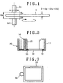
- sensors 2u, 2d are faced to both sides of the wafer 1 turnably held as shown in Fig.1, and distances Du, Dd from the sensors 2u, 2d to the surface of the wafer 1 are measured.
- the sensors 2u, 2d are a sensor of capacitance for measuring variations in capacitance between the wafer 1 and the sensor 2u, 2d, or an optical sensor for measuring a distance from the wafer 1 to the sensors 2u, 2d by means of a laser beam irradiated to and reflected on the surface of the wafer 1.
- a measured result is obtained as an average value in the surface area of the wafer which the measuring part of the sensor opposes and it has a high value in reproductivity, If a sensor whose measuring part has a large scope is used, a time of operating the whole surface of the wafer is saved and the reproductivity is further heightened.
- the wafer to be measured is chamfered and inclined at the edge part thereof. If the measuring part of the sensor faces this inclined portion, or one portion of the measuring part deviates from the edge, a measured value calculated by the capacitance is less than actual data. It is, therefore, necessary to oppose the measuring part of the sensor to the surface of the wafer so that the measuring part does not enter the edge part. Namely, the degree of flatness of the wafer is measured, leaving an insensitive zone depending on the area of the measuring part and existing around the periphery of the wafer, and such a part excepting the insensitive zone is cut to chips.
- the width of the insensitive zone present at the wafer periphery should be lessened as narrow as possible. Specifically, assuming that the wafer of the chamfered width being 0.5 mm is measured with the sensor of capacitance of a size being 4 mm x 4 mm, the reliability of data is lowered in the peripheral part inside 2.5 mm or more than the edge. This system can be employed in the present exception of the edge being determined at 3 mm, but cannot be responded to an inclination that the exception of the edge is made smaller for increasing the yield.
- the optical sensor is suitable for measuring a minute small area, and can measure nearly the edge.
- an object to be measured is a spot of about 1 to 2 ⁇ m diameter, it is practically impossible to measure the full surface of the wafer, and several points in the wafer surface cannot but be sampling-measured. Therefore, the reliability or reproductivity of measured results are low.
- the present invention has been devised to solve such problem and it is an object to give a function capable of measuring both large and small areas to the sensor, thereby to measure the degree of flatness of the wafer in the vicinity of the edge part exactly and in short time.
- the sensor for measuring the degree of flatness is characterized in that the sub sensor for measuring the small area is united in the main sensor of capacitance for measuring the large area.
- the sub sensor is united in the main sensor such that the main sensor and the sub sensor are on the same axis. Otherwise, the sub sensor is incorporated in the center of the main sensor.
- the sensor of capacitance which can obtain measured results of high reproductivity is employed.
- the sensor of capacitance of smaller size than that of the main sensor or the optical sensor which measures the surface area in spotting.
- the sensor according to the present invention integrally incorporates the sub sensor 20 for measuring the small area in the main sensor 10 for measuring the large area as shown in Fig.2.
- the sensor of capacitance having the same structure as a prior art is employed. Specifically, a measuring electrode 13 is mounted on a shielding case 11 via an insulating member 12. The measuring electrode 13 is connected to a detector through a leader wire 14. The circumference of the measuring electrode 13 is enclosed with guard ring 16 connected to an earth cable 15 for cutting off disturbances.
- the sub sensor 20 used are the sensor of capacitance for measuring the small area having the same structure as the main sensor 10, or an optical sensor 30 (Fig.3) suitable for measuring a minute area.
- the sensor integrally incorporated with the main sensor 10 and the sub sensor 20, as explained in Fig.1, moves to the radius of the wafer 1 under rotation, and scans all over the surface of the wafer 1 as drawing a helical locus, when relatively seeing.
- the sub sensor 20 moves along the same straight line as that of the main sensor 10, the sub sensor 20 is preferably unitary with the main sensor 10 such that the center line of the main sensor 10 accords with the center line of the sub sensor 20. Namely, for measuring the overall surface of the wafer 1, it is necessary to scan the wafer 1 while moving the sensor on the radius passing the center of the wafer If an off-set exists between the main sensor 10 and the sub sensor 20, the center of either off-set one of the sensors 10 or 20 cannot be measured. Otherwise, as shown in Fig.4, the sub sensor 20 may be incorporated in the center of the main sensor 10.
- the sub sensor 20 Apart near the edge of the wafer 1 is measured by the sub sensor 20, while a center thereof is measured by the main sensor 10.
- the edge portion of the chamfered wafer 1 is, as shown by enlarging in Fig.5, inclined from an edge E to a bevel starting point B, and the width E-B of the chamfered portion is generally determined to be around 0.5 mm.
- a point A where the measuring electrode 13 does not enter the bevel starting point B is determined to be a measuring critical point, and the width E-A is an insensitive zone.
- the measuring critical point A can be brought nearer to the beveling definition B, thereby widening an available area of the wafer 1.
- extension of a measuring time may be controlled.
- the sub sensor 20 may be also used for measuring the center of the wafer 1. Namely, since the sub sensor 20 deals with the measuring of the small area, it may be also used for variations in roughness in the surface. In this case, when both measured results obtained by the main sensor 10 and the sub sensor 20 are processed by a calculator, the data of the degree of flatness and the variation in roughness are obtained by once measurement.
- the same points may be concurrently measured without receiving influences of changes of measuring atmosphere (moisture, air flowing and others), so that measured results of high reliability are obtained.
- the wafer 1 where the flatness degree is measured is turnably supported within a vertical face, and the wafer 1 is scanned over the surface thereof with the sensors facing the surface and the reverse side of the wafer at the left and the right sides, influences such as bending deformation of the wafer 1 by gravity are removed, so that the measured results of high reliability are obtained.
- the flatness degree of the wafer 1 may be measured over the abroad area, and the measuring time is shortened.
- the sensor for measuring the degree of flatness has the structure incorporating the sub sensor in the main sensor, whereby the sub sensor dealing with the measuring of the small area measures the part near the edge part of the wafer Accordingly, the width of the insensitive zone can be made narrower in accordance with the size of the sub sensor, and the yield of the wafers to be cut into chips can be heightened, and the area of the available application can be widened.
Landscapes
- Physics & Mathematics (AREA)
- General Physics & Mathematics (AREA)
- Length Measuring Devices By Optical Means (AREA)
- Measurement Of Length, Angles, Or The Like Using Electric Or Magnetic Means (AREA)
- Length Measuring Devices With Unspecified Measuring Means (AREA)
Applications Claiming Priority (2)
| Application Number | Priority Date | Filing Date | Title |
|---|---|---|---|
| JP35811698 | 1998-12-16 | ||
| JP10358116A JP2000180157A (ja) | 1998-12-16 | 1998-12-16 | 平坦度測定センサ |
Publications (2)
| Publication Number | Publication Date |
|---|---|
| EP1010965A2 true EP1010965A2 (de) | 2000-06-21 |
| EP1010965A3 EP1010965A3 (de) | 2000-10-18 |
Family
ID=18457632
Family Applications (1)
| Application Number | Title | Priority Date | Filing Date |
|---|---|---|---|
| EP99106238A Withdrawn EP1010965A3 (de) | 1998-12-16 | 1999-04-13 | Sensor zur Erfassung des Planaritätsgrads |
Country Status (3)
| Country | Link |
|---|---|
| US (1) | US6255664B1 (de) |
| EP (1) | EP1010965A3 (de) |
| JP (1) | JP2000180157A (de) |
Cited By (1)
| Publication number | Priority date | Publication date | Assignee | Title |
|---|---|---|---|---|
| US20210333220A1 (en) * | 2017-11-29 | 2021-10-28 | Taiwan Semiconductor Manufacturing Co., Ltd. | Broadband wafer defect detection |
Families Citing this family (6)
| Publication number | Priority date | Publication date | Assignee | Title |
|---|---|---|---|---|
| US6768965B2 (en) * | 2002-04-18 | 2004-07-27 | Seh America, Inc. | Methods and computer program products for characterizing a crystalline structure |
| AT513245B1 (de) * | 2012-12-11 | 2014-03-15 | Siemens Vai Metals Tech Gmbh | Planheitsmessung und Messung der Eigenspannungen für ein metallisches Flachprodukt |
| KR20160111512A (ko) * | 2014-01-24 | 2016-09-26 | 도쿄엘렉트론가부시키가이샤 | 전방측 패터닝에 대한 조정을 결정하기 위한 후방측 기판 텍스처 맵을 발생시키는 시스템 및 방법 |
| DE102015012603A1 (de) * | 2015-09-28 | 2017-03-30 | Liebherr-Verzahntechnik Gmbh | Verfahren zum Entgraten eines Zahnradrohlings |
| CN111336914B (zh) * | 2020-03-25 | 2021-12-10 | 长江存储科技有限责任公司 | 晶圆翘曲度测量装置及方法 |
| CN116722226B (zh) * | 2023-06-28 | 2024-06-25 | 深圳市中天和自动化设备有限公司 | 一种锂电池封装装置 |
Citations (1)
| Publication number | Priority date | Publication date | Assignee | Title |
|---|---|---|---|---|
| US3990005A (en) * | 1974-09-03 | 1976-11-02 | Ade Corporation | Capacitive thickness gauging for ungrounded elements |
Family Cites Families (6)
| Publication number | Priority date | Publication date | Assignee | Title |
|---|---|---|---|---|
| US4183060A (en) * | 1976-03-19 | 1980-01-08 | Rca Corporation | Capacitance distance sensor apparatus for video disc player/recorder |
| JPS5744807A (en) * | 1980-08-29 | 1982-03-13 | Hitachi Ltd | Flatness measuring apparatus |
| US4476430A (en) * | 1982-04-05 | 1984-10-09 | Wright Wade S | Non-contact sensor for determining moving flat steel strip shape profile |
| US4560924A (en) * | 1983-07-22 | 1985-12-24 | Magnetic Peripherals Inc. | Flatness measuring apparatus |
| DE9004842U1 (de) * | 1990-04-28 | 1991-08-22 | Focus Meßtechnik GmbH & Co KG, 7505 Ettlingen | Oberflächenmeßgerät |
| US6062948A (en) * | 1996-04-19 | 2000-05-16 | Schmitt Measurement Systems, Inc. | Apparatus and method for gauging a workpiece |
-
1998
- 1998-12-16 JP JP10358116A patent/JP2000180157A/ja active Pending
-
1999
- 1999-04-05 US US09/286,712 patent/US6255664B1/en not_active Expired - Lifetime
- 1999-04-13 EP EP99106238A patent/EP1010965A3/de not_active Withdrawn
Patent Citations (1)
| Publication number | Priority date | Publication date | Assignee | Title |
|---|---|---|---|---|
| US3990005A (en) * | 1974-09-03 | 1976-11-02 | Ade Corporation | Capacitive thickness gauging for ungrounded elements |
Cited By (3)
| Publication number | Priority date | Publication date | Assignee | Title |
|---|---|---|---|---|
| US20210333220A1 (en) * | 2017-11-29 | 2021-10-28 | Taiwan Semiconductor Manufacturing Co., Ltd. | Broadband wafer defect detection |
| US11852593B2 (en) * | 2017-11-29 | 2023-12-26 | Taiwan Semiconductor Manufacturing Co., Ltd. | Broadband wafer defect detection |
| US12158434B2 (en) | 2017-11-29 | 2024-12-03 | Taiwan Semiconductor Manufacturing Co., Ltd. | Broadband wafer defect detection |
Also Published As
| Publication number | Publication date |
|---|---|
| EP1010965A3 (de) | 2000-10-18 |
| US6255664B1 (en) | 2001-07-03 |
| JP2000180157A (ja) | 2000-06-30 |
Similar Documents
| Publication | Publication Date | Title |
|---|---|---|
| US6528333B1 (en) | Method of and device for detecting micro-scratches | |
| US5291271A (en) | Measurement of transparent container wall thickness | |
| US5768335A (en) | Apparatus and method for measuring the orientation of a single crystal surface | |
| US6255664B1 (en) | Sensor for measuring degree of flatness | |
| US6016061A (en) | Cantilever type probe needle for probe card and method of fabrication and control thereof | |
| US20030041656A1 (en) | Method and apparatus for detecting topographical features of microelectronic substrates | |
| US3876879A (en) | Method and apparatus for determining surface characteristics incorporating a scanning electron microscope | |
| US6750977B2 (en) | Apparatus for monitoring thickness of deposited layer in reactor and dry processing method | |
| US20030073382A1 (en) | System and method for non-contact wear measurement of dicing saw blades | |
| US5790252A (en) | Method of and apparatus for determining residual damage to wafer edges | |
| US10365227B2 (en) | Detection device and detection method | |
| US5402239A (en) | Method of measuring orientation flat width of single crystal ingot | |
| US5936729A (en) | Photo detector assembly for measuring particle sizes | |
| JP3137160B2 (ja) | ウエハの位置ズレ補正方法 | |
| US5272342A (en) | Diffused layer depth measurement apparatus | |
| US5402001A (en) | Method of checking for foreign matter on a substrate with light of maximum reflectivity for that substrate | |
| US6473987B1 (en) | Method for measuring wafer thickness | |
| US4884887A (en) | Method for positioning a crystal ingot | |
| JP3951405B2 (ja) | 赤外顕微鏡 | |
| JP2563589B2 (ja) | 異物検査装置 | |
| JPH10177973A (ja) | ブレード変位検出装置 | |
| JPH0653100A (ja) | 半導体ウエハ及びその結晶方位検出方法 | |
| US4924297A (en) | Semiconductor device package structure | |
| JPH071780B2 (ja) | エピタキシャルウエーハの遷移領域の評価方法 | |
| JP2644257B2 (ja) | ビーム検出用ターゲット |
Legal Events
| Date | Code | Title | Description |
|---|---|---|---|
| PUAI | Public reference made under article 153(3) epc to a published international application that has entered the european phase |
Free format text: ORIGINAL CODE: 0009012 |
|
| AK | Designated contracting states |
Kind code of ref document: A2 Designated state(s): DE FR GB |
|
| AX | Request for extension of the european patent |
Free format text: AL;LT;LV;MK;RO;SI |
|
| PUAL | Search report despatched |
Free format text: ORIGINAL CODE: 0009013 |
|
| AK | Designated contracting states |
Kind code of ref document: A3 Designated state(s): AT BE CH CY DE DK ES FI FR GB GR IE IT LI LU MC NL PT SE |
|
| AX | Request for extension of the european patent |
Free format text: AL;LT;LV;MK;RO;SI |
|
| RIC1 | Information provided on ipc code assigned before grant |
Free format text: 7G 01B 7/34 A, 7G 01B 11/30 B |
|
| 17P | Request for examination filed |
Effective date: 20001229 |
|
| AKX | Designation fees paid |
Free format text: DE FR GB |
|
| 17Q | First examination report despatched |
Effective date: 20030728 |
|
| STAA | Information on the status of an ep patent application or granted ep patent |
Free format text: STATUS: THE APPLICATION IS DEEMED TO BE WITHDRAWN |
|
| 18D | Application deemed to be withdrawn |
Effective date: 20040210 |