EP1011028A2 - Verfahren zur Erzeugung von abgestuften Strukturen unter Einsatz von eingebetteten Ätzstopschichten - Google Patents
Verfahren zur Erzeugung von abgestuften Strukturen unter Einsatz von eingebetteten Ätzstopschichten Download PDFInfo
- Publication number
- EP1011028A2 EP1011028A2 EP99124935A EP99124935A EP1011028A2 EP 1011028 A2 EP1011028 A2 EP 1011028A2 EP 99124935 A EP99124935 A EP 99124935A EP 99124935 A EP99124935 A EP 99124935A EP 1011028 A2 EP1011028 A2 EP 1011028A2
- Authority
- EP
- European Patent Office
- Prior art keywords
- layer
- etch stop
- layers
- etching
- lens
- Prior art date
- Legal status (The legal status is an assumption and is not a legal conclusion. Google has not performed a legal analysis and makes no representation as to the accuracy of the status listed.)
- Granted
Links
- 238000000034 method Methods 0.000 title claims abstract description 65
- 238000004519 manufacturing process Methods 0.000 title abstract description 18
- 239000000463 material Substances 0.000 claims abstract description 89
- 238000005530 etching Methods 0.000 claims abstract description 38
- 238000000151 deposition Methods 0.000 claims abstract description 20
- 230000000873 masking effect Effects 0.000 claims abstract description 11
- 150000001875 compounds Chemical class 0.000 claims description 13
- 230000008569 process Effects 0.000 abstract description 31
- 238000000059 patterning Methods 0.000 abstract description 8
- 238000005137 deposition process Methods 0.000 abstract description 6
- 230000015572 biosynthetic process Effects 0.000 abstract description 4
- 239000000758 substrate Substances 0.000 description 11
- GQPLMRYTRLFLPF-UHFFFAOYSA-N Nitrous Oxide Chemical compound [O-][N+]#N GQPLMRYTRLFLPF-UHFFFAOYSA-N 0.000 description 4
- XUIMIQQOPSSXEZ-UHFFFAOYSA-N Silicon Chemical compound [Si] XUIMIQQOPSSXEZ-UHFFFAOYSA-N 0.000 description 4
- 239000000203 mixture Substances 0.000 description 4
- 238000000623 plasma-assisted chemical vapour deposition Methods 0.000 description 4
- 229910052710 silicon Inorganic materials 0.000 description 4
- 239000010703 silicon Substances 0.000 description 4
- QGZKDVFQNNGYKY-UHFFFAOYSA-N Ammonia Chemical compound N QGZKDVFQNNGYKY-UHFFFAOYSA-N 0.000 description 3
- 230000008901 benefit Effects 0.000 description 2
- 230000008859 change Effects 0.000 description 2
- 230000008021 deposition Effects 0.000 description 2
- 238000011065 in-situ storage Methods 0.000 description 2
- 239000001272 nitrous oxide Substances 0.000 description 2
- 230000003287 optical effect Effects 0.000 description 2
- 230000010363 phase shift Effects 0.000 description 2
- 238000004544 sputter deposition Methods 0.000 description 2
- 238000007738 vacuum evaporation Methods 0.000 description 2
- BLRPTPMANUNPDV-UHFFFAOYSA-N Silane Chemical compound [SiH4] BLRPTPMANUNPDV-UHFFFAOYSA-N 0.000 description 1
- 229910021529 ammonia Inorganic materials 0.000 description 1
- 229910021417 amorphous silicon Inorganic materials 0.000 description 1
- 239000007795 chemical reaction product Substances 0.000 description 1
- 230000001010 compromised effect Effects 0.000 description 1
- 238000007796 conventional method Methods 0.000 description 1
- 230000001934 delay Effects 0.000 description 1
- 230000001419 dependent effect Effects 0.000 description 1
- 239000011521 glass Substances 0.000 description 1
- 125000004435 hydrogen atom Chemical group [H]* 0.000 description 1
- 239000007788 liquid Substances 0.000 description 1
- 238000012986 modification Methods 0.000 description 1
- 230000004048 modification Effects 0.000 description 1
- 229910000069 nitrogen hydride Inorganic materials 0.000 description 1
- 238000000678 plasma activation Methods 0.000 description 1
- 239000010453 quartz Substances 0.000 description 1
- 230000005855 radiation Effects 0.000 description 1
- 229910000077 silane Inorganic materials 0.000 description 1
- VYPSYNLAJGMNEJ-UHFFFAOYSA-N silicon dioxide Inorganic materials O=[Si]=O VYPSYNLAJGMNEJ-UHFFFAOYSA-N 0.000 description 1
- 239000007787 solid Substances 0.000 description 1
- 238000009987 spinning Methods 0.000 description 1
Images

Classifications
-
- G—PHYSICS
- G03—PHOTOGRAPHY; CINEMATOGRAPHY; ANALOGOUS TECHNIQUES USING WAVES OTHER THAN OPTICAL WAVES; ELECTROGRAPHY; HOLOGRAPHY
- G03F—PHOTOMECHANICAL PRODUCTION OF TEXTURED OR PATTERNED SURFACES, e.g. FOR PRINTING, FOR PROCESSING OF SEMICONDUCTOR DEVICES; MATERIALS THEREFOR; ORIGINALS THEREFOR; APPARATUS SPECIALLY ADAPTED THEREFOR
- G03F7/00—Photomechanical, e.g. photolithographic, production of textured or patterned surfaces, e.g. printing surfaces; Materials therefor, e.g. comprising photoresists; Apparatus specially adapted therefor
- G03F7/0005—Production of optical devices or components in so far as characterised by the lithographic processes or materials used therefor
Definitions
- This invention relates to a method of fabrication for multi-step microlithographic structures. More particularly, the invention is directed to a method of fabrication for multi-step microlithographic structures (e.g. Fresnel lenses used in acoustic ink printing applications) whereby the process includes the formation of intermediate etch stop layers within the block from which the structure is formed.
- the method includes forming such layers by depositing etch material in-situ with Fresnel lens material. This is accomplished in the invention by depositing the lens material using known techniques and then selectively altering the chemistry of the material being deposited to form the intermediate etch stop layers at suitable positions without interrupting the deposition process.
- the etch stop layers are patterned between layers of lens material. In either case, the lens is then formed using masking, patterning and etching techniques.
- the invention is particularly directed to the art of fabrication of multi-step microlithographic structures including, as a specific example, Fresnel lens fabrication in the acoustic ink printing environment, and will thus be described with specific reference thereto, it will be appreciated that the invention may have usefulness in other fields and applications.
- the fabrication method also applies to Fresnel lenses or other multi-step microlithographic structures for use in, for example, optical, mechanical and electromechanical devices and is not limited to the acoustic ink printing environment.
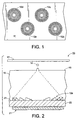
- Figure 1 shows a portion of an exemplary acoustic ink printhead 11 comprising an array of substantially identical multi-discrete-phase binary Fresnel acoustic focussing lenses 12a-d.
- This particular printhead configuration is well suited for certain types of printing, such as line printing, but it should be appreciated that such printheads (or substantially similar printheads) are also applicable to other pertinent configurations for implementing a variety of different print modes.
- the printhead 11 is embodied in an acoustic ink printer 13 for ejecting individual droplets of ink 14 from a free surface 15 of a pool of liquid ink 16 on demand at a sufficient ejection velocity to cause the droplets 14 to deposit in an image configuration on a nearby recording medium 17.
- the printhead 11 comprises a planar piezoelectric transducer 21 which is disposed on the rear face of an acoustically conductive substrate 22, such as a acoustically flat quartz, glass or silicon substrate.
- the opposite face of the substrate 22 has disposed thereon the concentric phase profiles of the Fresnel lens 12a which is generally representative of all lenses used. Sound waves are generated by the transducer 21 and focussed by the Fresnel lens toward the surface 15 of ink pool 16 to emit the droplets 14 therefrom.
- the representative lens 12a is a quantized approximation of the continuous phase profile of a theoretically ideal, 100% efficient, Fresnel phase plate. Accordingly, it will be evident that the acoustic focussing efficiency of the lens 12a and the width of its narrowest feature are dependent upon the number, n, of discrete phase levels to which its phase profiles is quantized. More specifically, two phase, four phase, eight phase and sixteen phase embodiments are approximately 41%, 81%, 95% and 99% efficient, respectively, for diffracting axial incident radiation into a focussed +1 diffraction order. A four phase Fresnel lens that is approximately 81% efficient has been determined to be acceptable for most acoustic ink printing applications.
- Fresnel lenses of the type noted herein that are in compliance with the design specifications of acoustic ink printing, for example.
- a four-phase Fresnel lens structure consists of three discrete steps.
- the thickness of each step may be determined by a time etch.
- uniformity may be compromised due to nonuniform etching characteristics resulting in over-etching and under-etching. Therefore, uniform etching is desired because overall ejector uniformity and Fresnel lens uniformity is critical to good print quality.
- uniformity and an economic and reliable process are also desired in applications other than Fresnel lens fabrication for acoustic ink printing.
- the present invention contemplates a new and improved fabrication method for multi-step microlithographic structures including Fresnel lenses used in, for example, acoustic ink printing applications and other such structures used in other applications which resolves the above referenced difficulties and others.
- a multi-step microlithographic structure fabrication method which uses intermediate etch stop layers that are embedded in the material of the structure.
- the method comprises steps of depositing a layer of a first material (onto a substrate) comprised of a plurality of elements or compounds supplied in first proportions, altering the first proportions of the plurality of elements or compounds to obtain a second material comprised of the plurality of elements or compounds supplied in second proportions, depositing an etch stop layer of the second material on the first material, altering the second proportions to again obtain the first material, and depositing another layer of the first material on the layer of the second material.
- steps may be selectively repeated to form a block having embedded etch stop layers from which the structure may be formed.
- etch stop layers are embedded between layers of material in a patterned fashion by depositing a layer of the first material and then patterning an etch stop layer thereon before depositing another layer of the first material.
- the process can be selectively repeated to build a block of material having embedded etch stop layers.
- the method includes selectively masking and etching the block to form the structure.
- the method is applied to fabrication of Fresnel lenses used in acoustic ink printing applications.
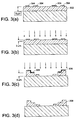
- FIGS. 3(a)-(d) show a cross-sectional slice of a single lens element
- a fabrication method for a four-phase Fresnel lens is shown.
- a film 302 is deposited whose thickness corresponds to a total height of the lens, e.g. 9 ⁇ m, and a mask 304 is patterned (Figure 3(a)).
- the mask comprises annular rings to correspond to the ring-like shape of the lenses as shown in Figure 1.
- the film is etched to a depth according to an n/2 phase shift, or about 3 ⁇ m, in the case of oxynitride ( Figure 3(b)).
- the first mask is then stripped off, a second mask 306 is patterned and etching continues for 6 ⁇ m to finally realize the four-phase Fresnel lens structure 308 ( Figures 3(c) and (d)).
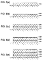
- FIGURES 5(a)-(e) provide an illustration of a process of depositing the lens material to form a block from which a four-phase Fresnel lens will be formed according to the present invention. While the description herein relates to a four-phase Fresnel lens which requires three layers of lens material and two etch stop layers, it is to be appreciated that the numbers of layers may be varied according to the number of phases of the Fresnel lens being formed.
- the material used to form the Fresnel lens is silicon oxynitride (SiON). It is also to be appreciated that various elements and/or compounds could be used as an alternative to silicon oxynitride. Nonetheless, to form the SiON material, the process includes the use of specified proportions of the following compounds: silane (SiH 4 ), nitrous oxide (N 2 O), and ammonia (NH 3 ). The reaction product resulting from the plasma activation of the mixture of these specified proportions causes deposition to build the primary portions of the block from which the lens will ultimately be formed.
- SiON silicon oxynitride
- these proportions of the compounds can be selectively altered to change the chemistry of that which is being deposited (SiON) to form a second material having a significantly slower etch rate.
- the second material is then deposited as etch stop layers.
- the advantage of this process is that the etch stop layers are formed during the deposition process in-situ with the lens material so no unnecessary interruptions and/or delays occur.
- the deposition process is preferably performed using a plasma enhanced chemical vapor deposition (PECVD) method.
- PECVD plasma enhanced chemical vapor deposition
- etch stop layers In the preferred PECVD process, plasma is used to release hydrogen atoms from the SiH 4 molecules so that the remaining free radicals will bond to form solid compounds (i.e. SiON).
- the chemistry of the plasma may be altered such that an etch resistant layer is deposited by, for example, increasing the flow of SiH 4 to provide a silicon rich oxynitride -- which etches much slower than the SiON.
- An amorphous silicon may also be formed as an etch stop layer.
- Figures 5(a)-(e) illustrate the deposition process that is used to form the substrate material that is ultimately patterned and etched to form a four-phase Fresnel lens according to the present invention.
- a layer 502 of SiON is first deposited on a substrate, preferably to a thickness of 3 ⁇ m ( Figure 5(a)).
- the proportions of the compounds comprising SiON are then altered, or chemistry thereof changed, to obtain a a second, slower etching material which is deposited in a layer 504, preferably to a thickness of about 0.1-0.2 ⁇ m ( Figure 5(b)).
- the chemistry of the etch stop material is altered back to the original SiON proportions to obtain SiON which is then deposited over the etch stop layer 504, preferably in a layer 506 having a thickness of approximately 3 ⁇ m (Figure 5(c)).
- the proportions of the materials used to form the SiON is again altered to obtain the second slower etching material which is deposited in a layer 508, preferably to a thickness of 0.1-0.2 ⁇ m ( Figure 5(d)).
- the chemistry is altered again in similar fashion and a layer 510 of SiON is deposited, preferably to a thickness of 3 ⁇ m ( Figure 5(e)).
- the altering of the compound proportions to change the chemistry of the material comprising the SiON and form an etch stop layer could be accomplished a number of different ways.
- the primary constraint on any such design choices is that the etch stop layer be of a composition that is etch resistant relative to the material that is being deposited as lens or primary material (e.g. SiON in the preferred embodiment).
- an n-phase Fresnel lens may be formed, not simply the exemplary 4-phase device.
- (n-1) substrate layers with intermediate etch stop layer should be formed.
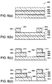
- FIGs 6(a)-(d) an example of a masking and etching process using the substrate similar to that formed in Figures 5(a)-(e) is shown. Only a portion of the material and a cross-sectional slice of only portions of two lens elements are shown. It is recognized that a variety of masking and etching processes could be used depending on the application and/or number of phases. The described process is but one such process.
- a mask 612 as well as masks 614 and 616, comprises annular ring portions corresponding to the ring-like shape of the lenses to be formed.
- the mask 612 is applied to the block 600 (i.e. layer 602) -- leaving areas unmasked or exposed -- and the SiON is etched (in areas corresponding to unmasked layers) until the etch stop layer 604 is encountered ( Figure 6(b)).
- the etch stop layer 604 will allow for over-etching because the etch stop layer 604 etches at a slower rate than the SiON of layer 602. So, any nonuniformity in etching can be accommodated because the etching of all of the SiON of layer 602 can be accomplished while the etching of the etch stop layer 604 proceeds but does not complete.
- the first mask 612 is removed.
- a second mask 614 is then patterned over the layers 602 and 604 and the etching of exposed areas continues by first etching through the remaining portions of the first etch stop layer 604 and then etching through the underlying portions of the layer 606 into the second etch stop layer 608 ( Figure 6(c)). Similar to encountering the first etch stop layer 604, encountering second etch stop layer 608 will compensate for the nonuniformities of etching the SiON layer 606.
- the second mask 614 is removed and a third mask 616 is patterned over layers 602, 604, 606 and 608 so that the etching of the remainder of exposed areas of the second etch stop layer 608 and the underlying SiON layer 610 can be completed ( Figure 6(d)).
- the process of etching through the etch stop layers to remove remaining portions thereof to expose underlying materials may be accomplished in a variety of manners.
- the same etch chemistry used for etching the lens material is used.
- the etch stop layer simply etches slower than the lens material. If it is desirable to increase the etch rate, the chemistry of the etching material could be altered.
- the etch technique could be changed for this process. For example, a plasma etch could be replaced with a wet etch technique for purposes of etching through the etch stop layer.
- An additional embodiment of the present invention involves the use of embedded etch stop layers as well.
- the etch stop layers are not formed by altering the chemistry of the material being deposited as the primary lens material. Rather, the etch stop layers are patterned onto layers of the primary lens material during formation of the block from which the lens is formed. Hard stops useful in the etching process are thus formed.
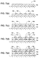
- a process 700 for forming a block of material is shown.
- a layer of lens material 702, having an etch rate is first deposited on a substrate ( Figure 7(a)).
- Deposition of the first material may be accomplished in a variety of ways including a PECVD process, sputter deposition or vacuum evaporation.
- a cross section of only a portion of the block being formed is shown.
- a pattern of a second, or etch stop, material 704 and 706 is formed using known masking and/or patterning techniques (Figure 7(b)).
- This pattern will be in the form of concentric rings (rings 704 and 706 shown) corresponding to the ring-like, or annular, shape of the Fresnel lens being formed.
- the etch rate of the second material is preferably substantially less than that of the first material. If desired, the second material may even be of a composition that it is not effectively etched in the etch process.
- Another layer of lens material 708 is then deposited ( Figure 7(c)).
- a second pattern of etch stop material is then masked/patterned ( Figure 7(d)). It should be appreciated that this pattern includes rings of etch stop material that are slightly offset from the rings on the lower layer of the block to accommodate for the stepped nature of the Fresnel lens being formed. So, as shown, rings 710 and 712 are patterned.
- a third layer of lens material 714 is deposited ( Figure 7(e)).
- any number of layers may be formed.
- any suitable material could be used. Any corresponding modifications or enhancements to the disclosed method based on any such alternatives will be appreciated by those skilled in the art.
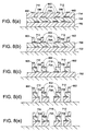
- the block formed in the process depicted in Figures 7(a)-(e) may be etched to form Fresnel lenses.
- Figures 8(a)-(e) show cross-sectional slices of two lens elements being formed.
- an appropriate annular pattern 802 is formed on the block using known techniques (Figure 8(a)).
- Exposed lens material is then etched away and the etch stop material (e.g. rings 710 and 712) is encountered ( Figure 8(b)).
- the second group of etch stop rings e.g. rings 704 and 706) is encountered ( Figure 8(c)).
- the initial mask 802 is then removed using known techniques (Figure 8(e)).
- the lens structures shown in Figure 8(e) include steps having the etch stop material remaining thereon.
- the etch stop layer may or may not be entirely intact at the end of the process, i.e. some portion may be etched away. In any event, it should be of a composition so that it is able to act as a mask throughout the etching process. It may also be desirable in some circumstances to remove the remaining exposed portions of the etch stop layers.
Landscapes
- Physics & Mathematics (AREA)
- General Physics & Mathematics (AREA)
- Particle Formation And Scattering Control In Inkjet Printers (AREA)
- Diffracting Gratings Or Hologram Optical Elements (AREA)
- Drying Of Semiconductors (AREA)
- Photosensitive Polymer And Photoresist Processing (AREA)
- Weting (AREA)
Applications Claiming Priority (2)
| Application Number | Priority Date | Filing Date | Title |
|---|---|---|---|
| US211781 | 1998-12-15 | ||
| US09/211,781 US6187211B1 (en) | 1998-12-15 | 1998-12-15 | Method for fabrication of multi-step structures using embedded etch stop layers |
Related Child Applications (1)
| Application Number | Title | Priority Date | Filing Date |
|---|---|---|---|
| EP11151918.7 Division-Into | 2011-01-24 |
Publications (3)
| Publication Number | Publication Date |
|---|---|
| EP1011028A2 true EP1011028A2 (de) | 2000-06-21 |
| EP1011028A3 EP1011028A3 (de) | 2004-12-01 |
| EP1011028B1 EP1011028B1 (de) | 2011-04-13 |
Family
ID=22788347
Family Applications (1)
| Application Number | Title | Priority Date | Filing Date |
|---|---|---|---|
| EP99124935A Expired - Lifetime EP1011028B1 (de) | 1998-12-15 | 1999-12-14 | Verfahren zur Erzeugung von abgestuften Strukturen unter Einsatz von eingebetteten Ätzstopschichten |
Country Status (5)
| Country | Link |
|---|---|
| US (1) | US6187211B1 (de) |
| EP (1) | EP1011028B1 (de) |
| JP (1) | JP2000181076A (de) |
| CA (1) | CA2288480C (de) |
| DE (1) | DE69943348D1 (de) |
Cited By (4)
| Publication number | Priority date | Publication date | Assignee | Title |
|---|---|---|---|---|
| WO2002071105A3 (en) * | 2000-12-05 | 2003-03-13 | Univ California | Method of fabricating reflection-mode euv diffraction elements |
| WO2008152058A1 (de) * | 2007-06-11 | 2008-12-18 | Endress+Hauser Flowtec Ag | Ultraschallsensor |
| US8741550B2 (en) | 2004-06-09 | 2014-06-03 | Schott Ag | Building up diffractive optics by structured glass coating |
| WO2019170523A1 (de) * | 2018-03-05 | 2019-09-12 | Osram Opto Semiconductors Gmbh | Verfahren zur herstellung eines mehrschichtoptikelements |
Families Citing this family (24)
| Publication number | Priority date | Publication date | Assignee | Title |
|---|---|---|---|---|
| JP4573418B2 (ja) * | 2000-10-04 | 2010-11-04 | リコー光学株式会社 | 露光方法 |
| US6596239B2 (en) * | 2000-12-12 | 2003-07-22 | Edc Biosystems, Inc. | Acoustically mediated fluid transfer methods and uses thereof |
| US6419803B1 (en) | 2001-03-16 | 2002-07-16 | 4Wave, Inc. | System and method for making thin-film structures using a stepped profile mask |
| US6976639B2 (en) | 2001-10-29 | 2005-12-20 | Edc Biosystems, Inc. | Apparatus and method for droplet steering |
| US6925856B1 (en) | 2001-11-07 | 2005-08-09 | Edc Biosystems, Inc. | Non-contact techniques for measuring viscosity and surface tension information of a liquid |
| US7205086B2 (en) * | 2001-11-26 | 2007-04-17 | E. I. Du Pont De Nemours And Company | Multilayer elements containing photoresist compositions and their use in microlithography |
| US7343535B2 (en) * | 2002-02-06 | 2008-03-11 | Avago Technologies General Ip Dte Ltd | Embedded testing capability for integrated serializer/deserializers |
| US6905618B2 (en) * | 2002-07-30 | 2005-06-14 | Agilent Technologies, Inc. | Diffractive optical elements and methods of making the same |
| US7275807B2 (en) * | 2002-11-27 | 2007-10-02 | Edc Biosystems, Inc. | Wave guide with isolated coupling interface |
| US7429359B2 (en) * | 2002-12-19 | 2008-09-30 | Edc Biosystems, Inc. | Source and target management system for high throughput transfer of liquids |
| US20050063648A1 (en) * | 2003-09-19 | 2005-03-24 | Wilson Robert Edward | Alignment post for optical subassemblies made with cylindrical rods, tubes, spheres, or similar features |
| US6947224B2 (en) * | 2003-09-19 | 2005-09-20 | Agilent Technologies, Inc. | Methods to make diffractive optical elements |
| US6953990B2 (en) * | 2003-09-19 | 2005-10-11 | Agilent Technologies, Inc. | Wafer-level packaging of optoelectronic devices |
| US6982437B2 (en) * | 2003-09-19 | 2006-01-03 | Agilent Technologies, Inc. | Surface emitting laser package having integrated optical element and alignment post |
| US7520679B2 (en) * | 2003-09-19 | 2009-04-21 | Avago Technologies Fiber Ip (Singapore) Pte. Ltd. | Optical device package with turning mirror and alignment post |
| US20050063431A1 (en) | 2003-09-19 | 2005-03-24 | Gallup Kendra J. | Integrated optics and electronics |
| US20050213995A1 (en) * | 2004-03-26 | 2005-09-29 | Myunghee Lee | Low power and low jitter optical receiver for fiber optic communication link |
| EP2232572A4 (de) * | 2007-12-07 | 2012-10-17 | Alion Inc | Fokussiertes akustisches bedrucken von strukturierten photovoltaikmaterialien |
| US20100184244A1 (en) * | 2009-01-20 | 2010-07-22 | SunPrint, Inc. | Systems and methods for depositing patterned materials for solar panel production |
| US8216939B2 (en) * | 2010-08-20 | 2012-07-10 | Micron Technology, Inc. | Methods of forming openings |
| CN103187265B (zh) * | 2011-12-31 | 2016-02-03 | 中芯国际集成电路制造(上海)有限公司 | 半导体器件的制造方法 |
| JP6652495B2 (ja) * | 2014-10-23 | 2020-02-26 | 株式会社ダイセル | フレネルレンズ、及びそれを備えた光学装置 |
| WO2016131069A2 (en) | 2015-12-11 | 2016-08-18 | Johnson Kenneth Carlisle | Euv light source with spectral purity filter and power recycling |
| JP2023105933A (ja) | 2022-01-20 | 2023-08-01 | 大日本印刷株式会社 | 回折格子、および回折格子形成用モールド |
Citations (3)
| Publication number | Priority date | Publication date | Assignee | Title |
|---|---|---|---|---|
| US4155627A (en) | 1976-02-02 | 1979-05-22 | Rca Corporation | Color diffractive subtractive filter master recording comprising a plurality of superposed two-level relief patterns on the surface of a substrate |
| JPH06258510A (ja) | 1993-03-09 | 1994-09-16 | Canon Inc | 回折格子製作用成形型およびその製造方法 |
| US5635423A (en) | 1994-10-11 | 1997-06-03 | Advanced Micro Devices, Inc. | Simplified dual damascene process for multi-level metallization and interconnection structure |
Family Cites Families (11)
| Publication number | Priority date | Publication date | Assignee | Title |
|---|---|---|---|---|
| JPS6266204A (ja) * | 1985-09-19 | 1987-03-25 | Pioneer Electronic Corp | フレネルレンズ及びその製造方法 |
| US4751529A (en) | 1986-12-19 | 1988-06-14 | Xerox Corporation | Microlenses for acoustic printing |
| US4751530A (en) | 1986-12-19 | 1988-06-14 | Xerox Corporation | Acoustic lens arrays for ink printing |
| US5161059A (en) * | 1987-09-21 | 1992-11-03 | Massachusetts Institute Of Technology | High-efficiency, multilevel, diffractive optical elements |
| US4895790A (en) * | 1987-09-21 | 1990-01-23 | Massachusetts Institute Of Technology | High-efficiency, multilevel, diffractive optical elements |
| US4944838A (en) * | 1989-08-03 | 1990-07-31 | At&T Bell Laboratories | Method of making tapered semiconductor waveguides |
| US5041849A (en) | 1989-12-26 | 1991-08-20 | Xerox Corporation | Multi-discrete-phase Fresnel acoustic lenses and their application to acoustic ink printing |
| JPH06160610A (ja) | 1989-12-26 | 1994-06-07 | Xerox Corp | 不連続多位相フレネルレンズ製造方法 |
| JPH0643311A (ja) * | 1992-07-22 | 1994-02-18 | Nippon Telegr & Teleph Corp <Ntt> | 回折光学素子及びその製造方法 |
| JPH0815510A (ja) * | 1994-06-30 | 1996-01-19 | Nikon Corp | バイナリーオプティクス及びその製造方法 |
| US5779751A (en) | 1997-03-14 | 1998-07-14 | Xerox Corporation | Photolithographic method of fabricating fresnel lenses |
-
1998
- 1998-12-15 US US09/211,781 patent/US6187211B1/en not_active Expired - Lifetime
-
1999
- 1999-11-02 CA CA002288480A patent/CA2288480C/en not_active Expired - Fee Related
- 1999-12-14 JP JP11354057A patent/JP2000181076A/ja active Pending
- 1999-12-14 EP EP99124935A patent/EP1011028B1/de not_active Expired - Lifetime
- 1999-12-14 DE DE69943348T patent/DE69943348D1/de not_active Expired - Lifetime
Patent Citations (3)
| Publication number | Priority date | Publication date | Assignee | Title |
|---|---|---|---|---|
| US4155627A (en) | 1976-02-02 | 1979-05-22 | Rca Corporation | Color diffractive subtractive filter master recording comprising a plurality of superposed two-level relief patterns on the surface of a substrate |
| JPH06258510A (ja) | 1993-03-09 | 1994-09-16 | Canon Inc | 回折格子製作用成形型およびその製造方法 |
| US5635423A (en) | 1994-10-11 | 1997-06-03 | Advanced Micro Devices, Inc. | Simplified dual damascene process for multi-level metallization and interconnection structure |
Cited By (6)
| Publication number | Priority date | Publication date | Assignee | Title |
|---|---|---|---|---|
| WO2002071105A3 (en) * | 2000-12-05 | 2003-03-13 | Univ California | Method of fabricating reflection-mode euv diffraction elements |
| US8741550B2 (en) | 2004-06-09 | 2014-06-03 | Schott Ag | Building up diffractive optics by structured glass coating |
| EP1754083B1 (de) * | 2004-06-09 | 2020-08-05 | Schott AG | Verfahren zur herstellung einer mehrlagigen fresnel-linse |
| WO2008152058A1 (de) * | 2007-06-11 | 2008-12-18 | Endress+Hauser Flowtec Ag | Ultraschallsensor |
| WO2019170523A1 (de) * | 2018-03-05 | 2019-09-12 | Osram Opto Semiconductors Gmbh | Verfahren zur herstellung eines mehrschichtoptikelements |
| US11067727B2 (en) | 2018-03-05 | 2021-07-20 | Osram Oled Gmbh | Method of manufacturing a multilayer optical element |
Also Published As
| Publication number | Publication date |
|---|---|
| DE69943348D1 (de) | 2011-05-26 |
| JP2000181076A (ja) | 2000-06-30 |
| CA2288480C (en) | 2004-03-30 |
| EP1011028A3 (de) | 2004-12-01 |
| CA2288480A1 (en) | 2000-06-15 |
| US6187211B1 (en) | 2001-02-13 |
| EP1011028B1 (de) | 2011-04-13 |
Similar Documents
| Publication | Publication Date | Title |
|---|---|---|
| US6187211B1 (en) | Method for fabrication of multi-step structures using embedded etch stop layers | |
| US5738757A (en) | Planar masking for multi-depth silicon etching | |
| US7837887B2 (en) | Method of forming an ink supply channel | |
| KR0170949B1 (ko) | 메탈층 형성 방법 | |
| CN112368639B (zh) | 衍射光栅的制造 | |
| JP5362060B2 (ja) | エピタキシャルリアクタにおける表面マイクロマシニングされた構造のためのギャップチューニング | |
| US8871648B2 (en) | Method for forming high density patterns | |
| US6713396B2 (en) | Method of fabricating high density sub-lithographic features on a substrate | |
| US20030087199A1 (en) | Method of manufacturing monolithic ink-jet printhead | |
| US7895750B2 (en) | Method of manufacturing inkjet print head | |
| KR20030011701A (ko) | 유체 공급 슬롯의 에칭 방법과 유체 방출 장치의 제조방법과 마이크로-유체 채널의 제조 방법 및 슬롯형 기판 | |
| US5487811A (en) | Process for preparation of semiconductor device | |
| US7524430B2 (en) | Fluid ejection device structures and methods therefor | |
| JP3851789B2 (ja) | マンドレルおよびそれを用いて電鋳するオリフィス板 | |
| EP1359609B1 (de) | Verfahren zur Herstellung einer sub-lithographischen Durchgangsleitung | |
| JP4533221B2 (ja) | タンタル層を形成する方法及びタンタル層を用いる装置 | |
| US20070020794A1 (en) | Method of strengthening a microscale chamber formed over a sacrificial layer | |
| AU2005254115B2 (en) | Process for modifying the surface profile of an ink supply channel in a printhead | |
| US20020134749A1 (en) | Method of making a vertical, mirror quality surface in silicon and mirror made by the method | |
| US6103318A (en) | Method for making an optical waveguide component using a low-stress silicon photomask | |
| WO2007016720A1 (en) | Method suitable for etching hydrophilic trenches in a substrate | |
| MXPA99011306A (en) | Method of forming a silicon layer on a surface | |
| KR20050056346A (ko) | 반도체소자의 워드라인 형성방법 |
Legal Events
| Date | Code | Title | Description |
|---|---|---|---|
| PUAI | Public reference made under article 153(3) epc to a published international application that has entered the european phase |
Free format text: ORIGINAL CODE: 0009012 |
|
| AK | Designated contracting states |
Kind code of ref document: A2 Designated state(s): AT BE CH CY DE DK ES FI FR GB GR IE IT LI LU MC NL PT SE |
|
| AX | Request for extension of the european patent |
Free format text: AL;LT;LV;MK;RO;SI |
|
| PUAL | Search report despatched |
Free format text: ORIGINAL CODE: 0009013 |
|
| AK | Designated contracting states |
Kind code of ref document: A3 Designated state(s): AT BE CH CY DE DK ES FI FR GB GR IE IT LI LU MC NL PT SE |
|
| AX | Request for extension of the european patent |
Extension state: AL LT LV MK RO SI |
|
| 17P | Request for examination filed |
Effective date: 20050601 |
|
| AKX | Designation fees paid |
Designated state(s): DE FR GB |
|
| 17Q | First examination report despatched |
Effective date: 20090114 |
|
| GRAP | Despatch of communication of intention to grant a patent |
Free format text: ORIGINAL CODE: EPIDOSNIGR1 |
|
| GRAS | Grant fee paid |
Free format text: ORIGINAL CODE: EPIDOSNIGR3 |
|
| GRAA | (expected) grant |
Free format text: ORIGINAL CODE: 0009210 |
|
| AK | Designated contracting states |
Kind code of ref document: B1 Designated state(s): DE FR GB |
|
| REG | Reference to a national code |
Ref country code: GB Ref legal event code: FG4D |
|
| REF | Corresponds to: |
Ref document number: 69943348 Country of ref document: DE Date of ref document: 20110526 Kind code of ref document: P |
|
| REG | Reference to a national code |
Ref country code: DE Ref legal event code: R096 Ref document number: 69943348 Country of ref document: DE Effective date: 20110526 |
|
| PLBE | No opposition filed within time limit |
Free format text: ORIGINAL CODE: 0009261 |
|
| STAA | Information on the status of an ep patent application or granted ep patent |
Free format text: STATUS: NO OPPOSITION FILED WITHIN TIME LIMIT |
|
| 26N | No opposition filed |
Effective date: 20120116 |
|
| REG | Reference to a national code |
Ref country code: DE Ref legal event code: R097 Ref document number: 69943348 Country of ref document: DE Effective date: 20120116 |
|
| REG | Reference to a national code |
Ref country code: FR Ref legal event code: PLFP Year of fee payment: 17 |
|
| REG | Reference to a national code |
Ref country code: FR Ref legal event code: PLFP Year of fee payment: 18 |
|
| REG | Reference to a national code |
Ref country code: FR Ref legal event code: PLFP Year of fee payment: 19 |
|
| PGFP | Annual fee paid to national office [announced via postgrant information from national office to epo] |
Ref country code: DE Payment date: 20171120 Year of fee payment: 19 Ref country code: FR Payment date: 20171121 Year of fee payment: 19 |
|
| PGFP | Annual fee paid to national office [announced via postgrant information from national office to epo] |
Ref country code: GB Payment date: 20171121 Year of fee payment: 19 |
|
| REG | Reference to a national code |
Ref country code: DE Ref legal event code: R119 Ref document number: 69943348 Country of ref document: DE |
|
| GBPC | Gb: european patent ceased through non-payment of renewal fee |
Effective date: 20181214 |
|
| PG25 | Lapsed in a contracting state [announced via postgrant information from national office to epo] |
Ref country code: DE Free format text: LAPSE BECAUSE OF NON-PAYMENT OF DUE FEES Effective date: 20190702 Ref country code: FR Free format text: LAPSE BECAUSE OF NON-PAYMENT OF DUE FEES Effective date: 20181231 |
|
| PG25 | Lapsed in a contracting state [announced via postgrant information from national office to epo] |
Ref country code: GB Free format text: LAPSE BECAUSE OF NON-PAYMENT OF DUE FEES Effective date: 20181214 |