EP1011131A1 - Procédé pour améliorer l'élimination d'un métal lors d'une étape de polissage méchano-chimique d'un semiconducteur - Google Patents
Procédé pour améliorer l'élimination d'un métal lors d'une étape de polissage méchano-chimique d'un semiconducteur Download PDFInfo
- Publication number
- EP1011131A1 EP1011131A1 EP99121400A EP99121400A EP1011131A1 EP 1011131 A1 EP1011131 A1 EP 1011131A1 EP 99121400 A EP99121400 A EP 99121400A EP 99121400 A EP99121400 A EP 99121400A EP 1011131 A1 EP1011131 A1 EP 1011131A1
- Authority
- EP
- European Patent Office
- Prior art keywords
- semiconductor wafer
- chemical
- acid
- mechanical polishing
- chelating agent
- Prior art date
- Legal status (The legal status is an assumption and is not a legal conclusion. Google has not performed a legal analysis and makes no representation as to the accuracy of the status listed.)
- Granted
Links
Images

Classifications
-
- C—CHEMISTRY; METALLURGY
- C09—DYES; PAINTS; POLISHES; NATURAL RESINS; ADHESIVES; COMPOSITIONS NOT OTHERWISE PROVIDED FOR; APPLICATIONS OF MATERIALS NOT OTHERWISE PROVIDED FOR
- C09K—MATERIALS FOR MISCELLANEOUS APPLICATIONS, NOT PROVIDED FOR ELSEWHERE
- C09K3/00—Materials not provided for elsewhere
- C09K3/14—Anti-slip materials; Abrasives
- C09K3/1454—Abrasive powders, suspensions and pastes for polishing
- C09K3/1463—Aqueous liquid suspensions
-
- H—ELECTRICITY
- H10—SEMICONDUCTOR DEVICES; ELECTRIC SOLID-STATE DEVICES NOT OTHERWISE PROVIDED FOR
- H10P—GENERIC PROCESSES OR APPARATUS FOR THE MANUFACTURE OR TREATMENT OF DEVICES COVERED BY CLASS H10
- H10P50/00—Etching of wafers, substrates or parts of devices
-
- H—ELECTRICITY
- H10—SEMICONDUCTOR DEVICES; ELECTRIC SOLID-STATE DEVICES NOT OTHERWISE PROVIDED FOR
- H10P—GENERIC PROCESSES OR APPARATUS FOR THE MANUFACTURE OR TREATMENT OF DEVICES COVERED BY CLASS H10
- H10P52/00—Grinding, lapping or polishing of wafers, substrates or parts of devices
- H10P52/40—Chemomechanical polishing [CMP]
- H10P52/403—Chemomechanical polishing [CMP] of conductive or resistive materials
-
- H—ELECTRICITY
- H10—SEMICONDUCTOR DEVICES; ELECTRIC SOLID-STATE DEVICES NOT OTHERWISE PROVIDED FOR
- H10W—GENERIC PACKAGES, INTERCONNECTIONS, CONNECTORS OR OTHER CONSTRUCTIONAL DETAILS OF DEVICES COVERED BY CLASS H10
- H10W20/00—Interconnections in chips, wafers or substrates
- H10W20/01—Manufacture or treatment
- H10W20/031—Manufacture or treatment of conductive parts of the interconnections
- H10W20/062—Manufacture or treatment of conductive parts of the interconnections by smoothing of conductive parts, e.g. by planarisation
-
- H—ELECTRICITY
- H10—SEMICONDUCTOR DEVICES; ELECTRIC SOLID-STATE DEVICES NOT OTHERWISE PROVIDED FOR
- H10P—GENERIC PROCESSES OR APPARATUS FOR THE MANUFACTURE OR TREATMENT OF DEVICES COVERED BY CLASS H10
- H10P14/00—Formation of materials, e.g. in the shape of layers or pillars
- H10P14/40—Formation of materials, e.g. in the shape of layers or pillars of conductive or resistive materials
- H10P14/418—Formation of materials, e.g. in the shape of layers or pillars of conductive or resistive materials the conductive layers comprising transition metals
Definitions
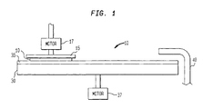
- the chemical-mechanical polishing process will involve holding the semiconductor wafer 10 against the rotating, wetted polishing surface of polishing pad 35.
- the polishing slurry is used to wet the polishing surface.
- the slurry may include a basic or acidic solution used as a chemical etch component in combination with an abrasive, such as alumina or silica particles.
- a rotating polishing head or the wafer carrier 15 is typically utilized to hold the wafer 10 against the rotating polishing platen 30 under controlled pressure.
- a backing film is optionally positioned between the wafer carrier 15 and the wafer.
- the polishing platen 30 is typically covered with a relatively soft wetted pad material such as blown polyurethane.
- the method involves providing a semiconductor wafer having an insulator layer, a metal barrier layer formed on at least a portion of the insulator layer and a conductive layer formed thereon and contacting the semiconductor wafer with a CMP slurry containing a metal removal-enhancing amount of a chelating agent to remove the metal barrier layer and conductive layer.
- the semiconductor wafer 8 is subjected to a standard CMP polishing process to advantageously remove the metal barrier layer 14 and the conductive layer 16 from the top surface of the insulator layer 12 to provide a substantially planar top surface of semiconductor wafer 8 as shown in FIG. 4.
- a CMP slurry will be used during the polishing process to remove the metal barrier layer 14 and the conductive layer 16 from the wafer 8.
- the slurry can be any conventional CMP slurry known to one skilled in the art.
- a preferred slurry for use herein include any alumina or silica based slurry, which can be basic or acidic. Conditions such as the amount of pressure and rotation speeds of the polishing platen to be used during the CMP process are within the purview of one skilled in the art.
- a CMP slurry containing a metal removal-enhancing amount of a chelating agent is contacted with the top surface of the wafer 8, i.e., the conductive layer 16, either in the first CMP step or in the touchup CMP step. It is highly advantageous to employ a chelating agent since the chelator will not increase or decrease the pH of the slurry.
- the wafer 8 can be contacted with the chelator during the CMP process to substantially remove the metal barrier layer 14 and the conductive layer 16 as part of the CMP slurry or, alternatively, simultaneously with the CMP slurry during the touchup CMP step to remove any residue remaining on the top surface of wafer 8 as discussed hereinabove.
- Chelating agents useful herein include polyphosphates such as sodium tripolyphosphate and hexenetaphosphoric acid; aminocarboxylic acids such as ethylenediaminetetraacetic acid (EDTA), hydroxyethylethylenediaminetriacetic acid (HEDTA), nitrilotriacetic acid (NTA), N-dihydroxyethylglycine and ethylene bis(hydroxyphenylglycine) (EHPG); 1,3-diketones such as acetylacetone, trifluoroacetylacetone and thenoyltrifluoroacetone (TTA); hydroxycarboxylic acids such as tartaric acid, citric acid, gluconic acid and 5-sulfosalicylic acid; polyamines such as ethylenediamine, triethylenediamine and triaminotriethylamine; aminoalcohols such as triethanolamine (TEA) and N-hydroxyethylethylenediamine; aromatic heterocyclic bases such as dipyrid
- the amount of chelators contacted with the wafer 8 should be a metal removal-enhancing amount. What constitutes a metal removal-enhancing amount of chelator will depend on a number of factors including, for example, the specific chelator used, the size of the wafer 8 and the composition and surface characteristics of the wafer 8. Typically, a metal removal-enhancing amount will ordinarily range from about 0.1 to about 30 weight percent, preferably from about 1 to about 20 weight percent, and more preferably from about 2 to about 10 weight percent. When employing the chelator in the CMP slurry to remove any remaining residue, the wafer 8 should be contacted with the chelator slurry for a time period ranging from about 5 to about 300 seconds and preferably from about 20 to about 100 seconds.
- the wafer 8 should be contacted with the chelator slurry for a time ranging from about 5 to about 400 seconds, preferably from about 20 to about 300 seconds and more preferably from about 100 to about 200 seconds when removing the metal barrier layer 14 and conductive layer 16.
- the temperature during contact with the chelator slurry need not be precisely controlled, but normally can range from about 0°C to about 50°C and more preferably from about 10°C to about 20°C.
Landscapes
- Chemical & Material Sciences (AREA)
- Engineering & Computer Science (AREA)
- Materials Engineering (AREA)
- Organic Chemistry (AREA)
- Mechanical Treatment Of Semiconductor (AREA)
- Internal Circuitry In Semiconductor Integrated Circuit Devices (AREA)
- Finish Polishing, Edge Sharpening, And Grinding By Specific Grinding Devices (AREA)
Applications Claiming Priority (2)
| Application Number | Priority Date | Filing Date | Title |
|---|---|---|---|
| US213469 | 1998-12-17 | ||
| US09/213,469 US6136714A (en) | 1998-12-17 | 1998-12-17 | Methods for enhancing the metal removal rate during the chemical-mechanical polishing process of a semiconductor |
Publications (2)
| Publication Number | Publication Date |
|---|---|
| EP1011131A1 true EP1011131A1 (fr) | 2000-06-21 |
| EP1011131B1 EP1011131B1 (fr) | 2007-07-25 |
Family
ID=22795239
Family Applications (1)
| Application Number | Title | Priority Date | Filing Date |
|---|---|---|---|
| EP99121400A Expired - Lifetime EP1011131B1 (fr) | 1998-12-17 | 1999-10-27 | Procédé pour améliorer l'élimination d'un métal lors d'une étape de polissage méchano-chimique d'un semiconducteur |
Country Status (7)
| Country | Link |
|---|---|
| US (1) | US6136714A (fr) |
| EP (1) | EP1011131B1 (fr) |
| JP (1) | JP2000183004A (fr) |
| KR (1) | KR100693640B1 (fr) |
| CN (1) | CN1257305A (fr) |
| DE (1) | DE69936625T2 (fr) |
| TW (1) | TW466640B (fr) |
Cited By (12)
| Publication number | Priority date | Publication date | Assignee | Title |
|---|---|---|---|---|
| EP1209731A1 (fr) * | 2000-11-24 | 2002-05-29 | Fujimi Incorporated | Composition de polissage et méthode de polissage l'employant |
| WO2002063669A3 (fr) * | 2000-10-27 | 2002-12-05 | Applied Materials Inc | Procede et appareil de polissage de couche barriere a deux etapes |
| US6524167B1 (en) | 2000-10-27 | 2003-02-25 | Applied Materials, Inc. | Method and composition for the selective removal of residual materials and barrier materials during substrate planarization |
| US6656842B2 (en) | 1999-09-22 | 2003-12-02 | Applied Materials, Inc. | Barrier layer buffing after Cu CMP |
| US6780773B2 (en) | 2001-07-11 | 2004-08-24 | Applied Materials Inc. | Method of chemical mechanical polishing with high throughput and low dishing |
| US6821881B2 (en) | 2001-07-25 | 2004-11-23 | Applied Materials, Inc. | Method for chemical mechanical polishing of semiconductor substrates |
| US6858540B2 (en) | 2000-05-11 | 2005-02-22 | Applied Materials, Inc. | Selective removal of tantalum-containing barrier layer during metal CMP |
| US7008554B2 (en) | 2001-07-13 | 2006-03-07 | Applied Materials, Inc. | Dual reduced agents for barrier removal in chemical mechanical polishing |
| US7012025B2 (en) | 2001-01-05 | 2006-03-14 | Applied Materials Inc. | Tantalum removal during chemical mechanical polishing |
| US7037174B2 (en) | 2002-10-03 | 2006-05-02 | Applied Materials, Inc. | Methods for reducing delamination during chemical mechanical polishing |
| US7104869B2 (en) | 2001-07-13 | 2006-09-12 | Applied Materials, Inc. | Barrier removal at low polish pressure |
| FR2898906A1 (fr) * | 2006-03-21 | 2007-09-28 | Kemesys | Composition de polissage mecano chimique incluant un alkylxanthate, procede de preparation et utilisation |
Families Citing this family (42)
| Publication number | Priority date | Publication date | Assignee | Title |
|---|---|---|---|---|
| US6896826B2 (en) * | 1997-01-09 | 2005-05-24 | Advanced Technology Materials, Inc. | Aqueous cleaning composition containing copper-specific corrosion inhibitor for cleaning inorganic residues on semiconductor substrate |
| US6068879A (en) * | 1997-08-26 | 2000-05-30 | Lsi Logic Corporation | Use of corrosion inhibiting compounds to inhibit corrosion of metal plugs in chemical-mechanical polishing |
| SG73683A1 (en) * | 1998-11-24 | 2000-06-20 | Texas Instruments Inc | Stabilized slurry compositions |
| JP4516176B2 (ja) * | 1999-04-20 | 2010-08-04 | 関東化学株式会社 | 電子材料用基板洗浄液 |
| US6274478B1 (en) * | 1999-07-13 | 2001-08-14 | Motorola, Inc. | Method for forming a copper interconnect using a multi-platen chemical mechanical polishing (CMP) process |
| US6573173B2 (en) | 1999-07-13 | 2003-06-03 | Motorola, Inc. | Method for forming a copper interconnect using a multi-platen chemical mechanical polishing (CMP) process |
| ATE405618T1 (de) * | 1999-08-13 | 2008-09-15 | Cabot Microelectronics Corp | Chemisch-mechanische poliersysteme und verfahren zu ihrer verwendung |
| US6855266B1 (en) * | 1999-08-13 | 2005-02-15 | Cabot Microelectronics Corporation | Polishing system with stopping compound and method of its use |
| US6436830B1 (en) * | 1999-10-06 | 2002-08-20 | Agere Systems Guardian Corp. | CMP system for polishing semiconductor wafers and related method |
| US6458289B1 (en) | 1999-10-06 | 2002-10-01 | Agere Systems Guardian Corp. | CMP slurry for polishing semiconductor wafers and related methods |
| US6368955B1 (en) * | 1999-11-22 | 2002-04-09 | Lucent Technologies, Inc. | Method of polishing semiconductor structures using a two-step chemical mechanical planarization with slurry particles having different particle bulk densities |
| US6638143B2 (en) | 1999-12-22 | 2003-10-28 | Applied Materials, Inc. | Ion exchange materials for chemical mechanical polishing |
| US6881674B2 (en) * | 1999-12-28 | 2005-04-19 | Intel Corporation | Abrasives for chemical mechanical polishing |
| JP2001269859A (ja) * | 2000-03-27 | 2001-10-02 | Jsr Corp | 化学機械研磨用水系分散体 |
| US6350692B1 (en) | 2000-12-14 | 2002-02-26 | Infineon Technologies Ag | Increased polish removal rate of dielectric layers using fixed abrasive pads |
| KR100407296B1 (ko) * | 2000-12-18 | 2003-11-28 | 주식회사 하이닉스반도체 | 티타늄알루미늄나이트라이드의 화학적기계적연마 방법 |
| US6783432B2 (en) | 2001-06-04 | 2004-08-31 | Applied Materials Inc. | Additives for pressure sensitive polishing compositions |
| US6482732B1 (en) * | 2001-06-29 | 2002-11-19 | Oki Electric Industry Co., Ltd. | Method and apparatus for polishing semiconductor wafer |
| US6805812B2 (en) | 2001-10-11 | 2004-10-19 | Cabot Microelectronics Corporation | Phosphono compound-containing polishing composition and method of using same |
| US6653224B1 (en) * | 2001-12-27 | 2003-11-25 | Lam Research Corporation | Methods for fabricating interconnect structures having Low K dielectric properties |
| JP4010903B2 (ja) * | 2002-08-02 | 2007-11-21 | Necエレクトロニクス株式会社 | 化学的機械的研磨用スラリー |
| US20040154931A1 (en) * | 2003-02-12 | 2004-08-12 | Akihisa Hongo | Polishing liquid, polishing method and polishing apparatus |
| USPP17182P3 (en) * | 2003-10-02 | 2006-11-07 | Plantas De Navarra S.A. | Peach tree plant named ‘Plawhite 5’ |
| US20050076579A1 (en) * | 2003-10-10 | 2005-04-14 | Siddiqui Junaid Ahmed | Bicine/tricine containing composition and method for chemical-mechanical planarization |
| US7390744B2 (en) | 2004-01-29 | 2008-06-24 | Applied Materials, Inc. | Method and composition for polishing a substrate |
| US7253111B2 (en) * | 2004-04-21 | 2007-08-07 | Rohm And Haas Electronic Materials Cmp Holding, Inc. | Barrier polishing solution |
| US20050252547A1 (en) * | 2004-05-11 | 2005-11-17 | Applied Materials, Inc. | Methods and apparatus for liquid chemical delivery |
| US20070205112A1 (en) * | 2004-08-27 | 2007-09-06 | Masako Kodera | Polishing apparatus and polishing method |
| WO2006022452A2 (fr) * | 2004-08-27 | 2006-03-02 | Ebara Corporation | Procede et appareil de polissage |
| JP4027929B2 (ja) * | 2004-11-30 | 2007-12-26 | 花王株式会社 | 半導体基板用研磨液組成物 |
| BRPI0518420A2 (pt) * | 2004-12-10 | 2008-11-25 | Mallinckrodt Baker Inc | composiÇÕes de limpeza de microeletrânicos nço-aquosas, nço-corrosivas, contendo inibidores de corrosço polimÉricos |
| WO2006125462A1 (fr) * | 2005-05-25 | 2006-11-30 | Freescale Semiconductor, Inc | Solution de nettoyage pour tranche de semi-conducteur |
| KR20070041330A (ko) * | 2005-10-14 | 2007-04-18 | 가오가부시끼가이샤 | 반도체 기판용 연마액 조성물 |
| US20100273330A1 (en) * | 2006-08-23 | 2010-10-28 | Citibank N.A. As Collateral Agent | Rinse formulation for use in the manufacture of an integrated circuit |
| JP2008074990A (ja) * | 2006-09-22 | 2008-04-03 | Nihon Micro Coating Co Ltd | 研磨スラリー及び方法 |
| JP2009088486A (ja) * | 2007-08-29 | 2009-04-23 | Applied Materials Inc | 高スループット低形状銅cmp処理 |
| JP5379441B2 (ja) * | 2008-10-09 | 2013-12-25 | 関東化学株式会社 | 基板処理用アルカリ性水溶液組成物 |
| JP5767898B2 (ja) * | 2011-08-12 | 2015-08-26 | 株式会社東芝 | 半導体装置の製造方法 |
| CN103474395B (zh) * | 2013-09-13 | 2016-08-24 | 华进半导体封装先导技术研发中心有限公司 | 一种tsv平坦化方法 |
| KR102544643B1 (ko) * | 2015-12-23 | 2023-06-19 | 솔브레인 주식회사 | 연마 슬러리 조성물 및 이를 이용한 연마방법 |
| KR101698168B1 (ko) * | 2016-06-02 | 2017-01-20 | 에버테크노 주식회사 | Agv를 이용한 번인 랙 이송장치 |
| CN116875194A (zh) * | 2023-05-18 | 2023-10-13 | 万华化学集团电子材料有限公司 | 一种钨化学机械抛光液及其应用 |
Citations (6)
| Publication number | Priority date | Publication date | Assignee | Title |
|---|---|---|---|---|
| WO1997043087A1 (fr) * | 1996-05-10 | 1997-11-20 | Cabot Corporation | Pate liquide de polissage mecano-chimique pour couches metalliques et couches minces |
| US5700383A (en) * | 1995-12-21 | 1997-12-23 | Intel Corporation | Slurries and methods for chemical mechanical polish of aluminum and titanium aluminide |
| US5735963A (en) * | 1996-12-17 | 1998-04-07 | Lucent Technologies Inc. | Method of polishing |
| US5770095A (en) * | 1994-07-12 | 1998-06-23 | Kabushiki Kaisha Toshiba | Polishing agent and polishing method using the same |
| US5836806A (en) * | 1993-11-03 | 1998-11-17 | Intel Corporation | Slurries for chemical mechanical polishing |
| WO1998053488A1 (fr) * | 1997-05-20 | 1998-11-26 | Rodel Holdings, Inc. | Procede de polissage d'un materiau composite comprenant un isolant, un metal et du titane |
Family Cites Families (4)
| Publication number | Priority date | Publication date | Assignee | Title |
|---|---|---|---|---|
| US5084071A (en) * | 1989-03-07 | 1992-01-28 | International Business Machines Corporation | Method of chemical-mechanical polishing an electronic component substrate and polishing slurry therefor |
| JPH0982668A (ja) * | 1995-09-20 | 1997-03-28 | Sony Corp | 研磨用スラリー及びこの研磨用スラリーを用いる研磨方法 |
| KR100257427B1 (ko) * | 1996-05-31 | 2000-05-15 | 아사무라 타카싯 | 반도체기판표면을연마하여평탄한표면형상을형성하기위한반도체기판연마방법 |
| US5783489A (en) * | 1996-09-24 | 1998-07-21 | Cabot Corporation | Multi-oxidizer slurry for chemical mechanical polishing |
-
1998
- 1998-12-17 US US09/213,469 patent/US6136714A/en not_active Expired - Lifetime
-
1999
- 1999-10-27 DE DE69936625T patent/DE69936625T2/de not_active Expired - Lifetime
- 1999-10-27 EP EP99121400A patent/EP1011131B1/fr not_active Expired - Lifetime
- 1999-10-28 TW TW088118683A patent/TW466640B/zh not_active IP Right Cessation
- 1999-12-16 CN CN99126529A patent/CN1257305A/zh active Pending
- 1999-12-16 KR KR1019990058140A patent/KR100693640B1/ko not_active Expired - Fee Related
- 1999-12-17 JP JP11359334A patent/JP2000183004A/ja not_active Withdrawn
Patent Citations (6)
| Publication number | Priority date | Publication date | Assignee | Title |
|---|---|---|---|---|
| US5836806A (en) * | 1993-11-03 | 1998-11-17 | Intel Corporation | Slurries for chemical mechanical polishing |
| US5770095A (en) * | 1994-07-12 | 1998-06-23 | Kabushiki Kaisha Toshiba | Polishing agent and polishing method using the same |
| US5700383A (en) * | 1995-12-21 | 1997-12-23 | Intel Corporation | Slurries and methods for chemical mechanical polish of aluminum and titanium aluminide |
| WO1997043087A1 (fr) * | 1996-05-10 | 1997-11-20 | Cabot Corporation | Pate liquide de polissage mecano-chimique pour couches metalliques et couches minces |
| US5735963A (en) * | 1996-12-17 | 1998-04-07 | Lucent Technologies Inc. | Method of polishing |
| WO1998053488A1 (fr) * | 1997-05-20 | 1998-11-26 | Rodel Holdings, Inc. | Procede de polissage d'un materiau composite comprenant un isolant, un metal et du titane |
Cited By (19)
| Publication number | Priority date | Publication date | Assignee | Title |
|---|---|---|---|---|
| US6656842B2 (en) | 1999-09-22 | 2003-12-02 | Applied Materials, Inc. | Barrier layer buffing after Cu CMP |
| US6858540B2 (en) | 2000-05-11 | 2005-02-22 | Applied Materials, Inc. | Selective removal of tantalum-containing barrier layer during metal CMP |
| WO2002063669A3 (fr) * | 2000-10-27 | 2002-12-05 | Applied Materials Inc | Procede et appareil de polissage de couche barriere a deux etapes |
| US6524167B1 (en) | 2000-10-27 | 2003-02-25 | Applied Materials, Inc. | Method and composition for the selective removal of residual materials and barrier materials during substrate planarization |
| US6709316B1 (en) | 2000-10-27 | 2004-03-23 | Applied Materials, Inc. | Method and apparatus for two-step barrier layer polishing |
| US6838016B2 (en) | 2000-11-24 | 2005-01-04 | Fujimi Incorporated | Polishing composition and polishing method employing it |
| EP1209731A1 (fr) * | 2000-11-24 | 2002-05-29 | Fujimi Incorporated | Composition de polissage et méthode de polissage l'employant |
| US7012025B2 (en) | 2001-01-05 | 2006-03-14 | Applied Materials Inc. | Tantalum removal during chemical mechanical polishing |
| US6780773B2 (en) | 2001-07-11 | 2004-08-24 | Applied Materials Inc. | Method of chemical mechanical polishing with high throughput and low dishing |
| US6790768B2 (en) | 2001-07-11 | 2004-09-14 | Applied Materials Inc. | Methods and apparatus for polishing substrates comprising conductive and dielectric materials with reduced topographical defects |
| US6960521B2 (en) | 2001-07-11 | 2005-11-01 | Applied Materials, Inc. | Method and apparatus for polishing metal and dielectric substrates |
| US7232761B2 (en) | 2001-07-11 | 2007-06-19 | Applied Materials, Inc. | Method of chemical mechanical polishing with high throughput and low dishing |
| US7008554B2 (en) | 2001-07-13 | 2006-03-07 | Applied Materials, Inc. | Dual reduced agents for barrier removal in chemical mechanical polishing |
| US7104869B2 (en) | 2001-07-13 | 2006-09-12 | Applied Materials, Inc. | Barrier removal at low polish pressure |
| US6821881B2 (en) | 2001-07-25 | 2004-11-23 | Applied Materials, Inc. | Method for chemical mechanical polishing of semiconductor substrates |
| US7060606B2 (en) | 2001-07-25 | 2006-06-13 | Applied Materials Inc. | Method and apparatus for chemical mechanical polishing of semiconductor substrates |
| US7037174B2 (en) | 2002-10-03 | 2006-05-02 | Applied Materials, Inc. | Methods for reducing delamination during chemical mechanical polishing |
| US7244168B2 (en) | 2002-10-03 | 2007-07-17 | Applied Materials, Inc. | Methods for reducing delamination during chemical mechanical polishing |
| FR2898906A1 (fr) * | 2006-03-21 | 2007-09-28 | Kemesys | Composition de polissage mecano chimique incluant un alkylxanthate, procede de preparation et utilisation |
Also Published As
| Publication number | Publication date |
|---|---|
| KR20000048170A (ko) | 2000-07-25 |
| CN1257305A (zh) | 2000-06-21 |
| DE69936625D1 (de) | 2007-09-06 |
| TW466640B (en) | 2001-12-01 |
| JP2000183004A (ja) | 2000-06-30 |
| EP1011131B1 (fr) | 2007-07-25 |
| KR100693640B1 (ko) | 2007-03-14 |
| US6136714A (en) | 2000-10-24 |
| DE69936625T2 (de) | 2008-01-31 |
Similar Documents
| Publication | Publication Date | Title |
|---|---|---|
| US6136714A (en) | Methods for enhancing the metal removal rate during the chemical-mechanical polishing process of a semiconductor | |
| US5786275A (en) | Process of fabricating wiring structure having metal plug twice polished under different conditions | |
| Steigerwald et al. | Pattern Geometry Effects in the Chemical‐Mechanical Polishing of Inlaid Copper Structures | |
| EP0747939B1 (fr) | Solution de polissage pour métaux à base de cuivre et procédé de fabrication d'un dispositif semi-conducteur | |
| US5872043A (en) | Method of planarizing wafers with shallow trench isolation | |
| US6423640B1 (en) | Headless CMP process for oxide planarization | |
| KR0183826B1 (ko) | 연마공정 후처리용 세정 용액 및 그를 이용하는 세정 방법 | |
| US20020061635A1 (en) | Solution for chemical mechanical polishing and method of manufacturing copper metal interconnection layer using the same | |
| US7041600B2 (en) | Methods of planarization | |
| EP1004648A1 (fr) | Améliorations aux ou relatives aux dispositifs semi-conducteurs | |
| US7510974B2 (en) | CMP process | |
| WO2001013425A1 (fr) | Fabrication de structures isolantes pour ci | |
| US6114215A (en) | Generating non-planar topology on the surface of planar and near-planar substrates | |
| JP3872925B2 (ja) | 研磨装置および半導体装置の製造方法 | |
| US20080220585A1 (en) | Method of manufacturing a semiconductor device | |
| US6534407B2 (en) | Method for reducing dishing effects during a chemical mechanical polishing process | |
| US20030124861A1 (en) | Method for manufacturing metal line contact plug semiconductor device | |
| HK1025668A (en) | Methods for enhancing the metal removal rate during the chemical-mechanical polishing process of a semiconductor | |
| US6607967B1 (en) | Process for forming planarized isolation trench in integrated circuit structure on semiconductor substrate | |
| US6190999B1 (en) | Method for fabricating a shallow trench isolation structure | |
| US6235071B1 (en) | Chemical mechanical polishing method for highly accurate in-plane uniformity in polishing rate over position | |
| US6358850B1 (en) | Slurry-less chemical-mechanical polishing of oxide materials | |
| KR100645841B1 (ko) | 연마정지막을 이용한 폴리실리콘 플러그 형성 방법 | |
| US6645825B1 (en) | Planarization of shallow trench isolation (STI) | |
| WO2002024413A2 (fr) | Polissage par cmp pour planarisation optimisee |
Legal Events
| Date | Code | Title | Description |
|---|---|---|---|
| PUAI | Public reference made under article 153(3) epc to a published international application that has entered the european phase |
Free format text: ORIGINAL CODE: 0009012 |
|
| AK | Designated contracting states |
Kind code of ref document: A1 Designated state(s): DE FR GB IE IT NL |
|
| AX | Request for extension of the european patent |
Free format text: AL;LT;LV;MK;RO;SI |
|
| RIN1 | Information on inventor provided before grant (corrected) |
Inventor name: SCHUTZ, RONALD JOSEPH |
|
| RIN1 | Information on inventor provided before grant (corrected) |
Inventor name: SCHUTZ, RONALD JOSEPH |
|
| 17P | Request for examination filed |
Effective date: 20000919 |
|
| AKX | Designation fees paid |
Free format text: DE FR GB IE IT NL |
|
| 17Q | First examination report despatched |
Effective date: 20030912 |
|
| RAP1 | Party data changed (applicant data changed or rights of an application transferred) |
Owner name: INFINEON TECHNOLOGIES AG |
|
| 17Q | First examination report despatched |
Effective date: 20030912 |
|
| GRAC | Information related to communication of intention to grant a patent modified |
Free format text: ORIGINAL CODE: EPIDOSCIGR1 |
|
| GRAP | Despatch of communication of intention to grant a patent |
Free format text: ORIGINAL CODE: EPIDOSNIGR1 |
|
| GRAS | Grant fee paid |
Free format text: ORIGINAL CODE: EPIDOSNIGR3 |
|
| REG | Reference to a national code |
Ref country code: HK Ref legal event code: WD Ref document number: 1025668 Country of ref document: HK |
|
| GRAA | (expected) grant |
Free format text: ORIGINAL CODE: 0009210 |
|
| AK | Designated contracting states |
Kind code of ref document: B1 Designated state(s): DE FR GB IE IT NL |
|
| REG | Reference to a national code |
Ref country code: GB Ref legal event code: FG4D |
|
| RIN2 | Information on inventor provided after grant (corrected) |
Inventor name: SCHUTZ, RONALD JOSEPH |
|
| REG | Reference to a national code |
Ref country code: IE Ref legal event code: FG4D |
|
| REF | Corresponds to: |
Ref document number: 69936625 Country of ref document: DE Date of ref document: 20070906 Kind code of ref document: P |
|
| PG25 | Lapsed in a contracting state [announced via postgrant information from national office to epo] |
Ref country code: NL Free format text: LAPSE BECAUSE OF FAILURE TO SUBMIT A TRANSLATION OF THE DESCRIPTION OR TO PAY THE FEE WITHIN THE PRESCRIBED TIME-LIMIT Effective date: 20070725 |
|
| NLV1 | Nl: lapsed or annulled due to failure to fulfill the requirements of art. 29p and 29m of the patents act | ||
| EN | Fr: translation not filed | ||
| PLBE | No opposition filed within time limit |
Free format text: ORIGINAL CODE: 0009261 |
|
| STAA | Information on the status of an ep patent application or granted ep patent |
Free format text: STATUS: NO OPPOSITION FILED WITHIN TIME LIMIT |
|
| GBPC | Gb: european patent ceased through non-payment of renewal fee |
Effective date: 20071027 |
|
| 26N | No opposition filed |
Effective date: 20080428 |
|
| PG25 | Lapsed in a contracting state [announced via postgrant information from national office to epo] |
Ref country code: FR Free format text: LAPSE BECAUSE OF FAILURE TO SUBMIT A TRANSLATION OF THE DESCRIPTION OR TO PAY THE FEE WITHIN THE PRESCRIBED TIME-LIMIT Effective date: 20080321 |
|
| PG25 | Lapsed in a contracting state [announced via postgrant information from national office to epo] |
Ref country code: IE Free format text: LAPSE BECAUSE OF NON-PAYMENT OF DUE FEES Effective date: 20071030 |
|
| PG25 | Lapsed in a contracting state [announced via postgrant information from national office to epo] |
Ref country code: GB Free format text: LAPSE BECAUSE OF NON-PAYMENT OF DUE FEES Effective date: 20071027 |
|
| PG25 | Lapsed in a contracting state [announced via postgrant information from national office to epo] |
Ref country code: IT Free format text: LAPSE BECAUSE OF NON-PAYMENT OF DUE FEES Effective date: 20071031 |
|
| PGFP | Annual fee paid to national office [announced via postgrant information from national office to epo] |
Ref country code: DE Payment date: 20141022 Year of fee payment: 16 |
|
| REG | Reference to a national code |
Ref country code: DE Ref legal event code: R081 Ref document number: 69936625 Country of ref document: DE Owner name: POLARIS INNOVATIONS LTD., IE Free format text: FORMER OWNER: QIMONDA AG, 81739 MUENCHEN, DE Ref country code: DE Ref legal event code: R081 Ref document number: 69936625 Country of ref document: DE Owner name: INFINEON TECHNOLOGIES AG, DE Free format text: FORMER OWNER: QIMONDA AG, 81739 MUENCHEN, DE |
|
| REG | Reference to a national code |
Ref country code: DE Ref legal event code: R081 Ref document number: 69936625 Country of ref document: DE Owner name: POLARIS INNOVATIONS LTD., IE Free format text: FORMER OWNER: INFINEON TECHNOLOGIES AG, 85579 NEUBIBERG, DE |
|
| REG | Reference to a national code |
Ref country code: DE Ref legal event code: R119 Ref document number: 69936625 Country of ref document: DE |
|
| PG25 | Lapsed in a contracting state [announced via postgrant information from national office to epo] |
Ref country code: DE Free format text: LAPSE BECAUSE OF NON-PAYMENT OF DUE FEES Effective date: 20160503 |