EP1011134A1 - Kontaktor für Halbleiterbauelemente, Testvorrichtung mit solchem Kontaktor, Testverfahren mit solchem Kontaktor und Reinigungsverfahren für solchen Kontaktor - Google Patents
Kontaktor für Halbleiterbauelemente, Testvorrichtung mit solchem Kontaktor, Testverfahren mit solchem Kontaktor und Reinigungsverfahren für solchen Kontaktor Download PDFInfo
- Publication number
- EP1011134A1 EP1011134A1 EP99306225A EP99306225A EP1011134A1 EP 1011134 A1 EP1011134 A1 EP 1011134A1 EP 99306225 A EP99306225 A EP 99306225A EP 99306225 A EP99306225 A EP 99306225A EP 1011134 A1 EP1011134 A1 EP 1011134A1
- Authority
- EP
- European Patent Office
- Prior art keywords
- wiring substrate
- contactor
- base unit
- semiconductor device
- seal member
- Prior art date
- Legal status (The legal status is an assumption and is not a legal conclusion. Google has not performed a legal analysis and makes no representation as to the accuracy of the status listed.)
- Granted
Links
Images







Classifications
-
- H—ELECTRICITY
- H10—SEMICONDUCTOR DEVICES; ELECTRIC SOLID-STATE DEVICES NOT OTHERWISE PROVIDED FOR
- H10P—GENERIC PROCESSES OR APPARATUS FOR THE MANUFACTURE OR TREATMENT OF DEVICES COVERED BY CLASS H10
- H10P74/00—Testing or measuring during manufacture or treatment of wafers, substrates or devices
-
- H—ELECTRICITY
- H10—SEMICONDUCTOR DEVICES; ELECTRIC SOLID-STATE DEVICES NOT OTHERWISE PROVIDED FOR
- H10P—GENERIC PROCESSES OR APPARATUS FOR THE MANUFACTURE OR TREATMENT OF DEVICES COVERED BY CLASS H10
- H10P72/00—Handling or holding of wafers, substrates or devices during manufacture or treatment thereof
- H10P72/70—Handling or holding of wafers, substrates or devices during manufacture or treatment thereof for supporting or gripping
- H10P72/78—Handling or holding of wafers, substrates or devices during manufacture or treatment thereof for supporting or gripping using vacuum or suction, e.g. Bernoulli chucks
-
- G—PHYSICS
- G01—MEASURING; TESTING
- G01R—MEASURING ELECTRIC VARIABLES; MEASURING MAGNETIC VARIABLES
- G01R31/00—Arrangements for testing electric properties; Arrangements for locating electric faults; Arrangements for electrical testing characterised by what is being tested not provided for elsewhere
- G01R31/28—Testing of electronic circuits, e.g. by signal tracer
- G01R31/2851—Testing of integrated circuits [IC]
- G01R31/2886—Features relating to contacting the IC under test, e.g. probe heads; chucks
-
- H—ELECTRICITY
- H10—SEMICONDUCTOR DEVICES; ELECTRIC SOLID-STATE DEVICES NOT OTHERWISE PROVIDED FOR
- H10P—GENERIC PROCESSES OR APPARATUS FOR THE MANUFACTURE OR TREATMENT OF DEVICES COVERED BY CLASS H10
- H10P72/00—Handling or holding of wafers, substrates or devices during manufacture or treatment thereof
- H10P72/04—Apparatus for manufacture or treatment
- H10P72/0441—Apparatus for sealing, encapsulating, glassing, decapsulating or the like
-
- H—ELECTRICITY
- H10—SEMICONDUCTOR DEVICES; ELECTRIC SOLID-STATE DEVICES NOT OTHERWISE PROVIDED FOR
- H10P—GENERIC PROCESSES OR APPARATUS FOR THE MANUFACTURE OR TREATMENT OF DEVICES COVERED BY CLASS H10
- H10P72/00—Handling or holding of wafers, substrates or devices during manufacture or treatment thereof
- H10P72/70—Handling or holding of wafers, substrates or devices during manufacture or treatment thereof for supporting or gripping
- H10P72/76—Handling or holding of wafers, substrates or devices during manufacture or treatment thereof for supporting or gripping using mechanical means, e.g. clamps or pinches
- H10P72/7604—Handling or holding of wafers, substrates or devices during manufacture or treatment thereof for supporting or gripping using mechanical means, e.g. clamps or pinches the wafers being placed on a susceptor, stage or support
- H10P72/7611—Handling or holding of wafers, substrates or devices during manufacture or treatment thereof for supporting or gripping using mechanical means, e.g. clamps or pinches the wafers being placed on a susceptor, stage or support characterised by edge profile or support profile
-
- H—ELECTRICITY
- H10—SEMICONDUCTOR DEVICES; ELECTRIC SOLID-STATE DEVICES NOT OTHERWISE PROVIDED FOR
- H10P—GENERIC PROCESSES OR APPARATUS FOR THE MANUFACTURE OR TREATMENT OF DEVICES COVERED BY CLASS H10
- H10P72/00—Handling or holding of wafers, substrates or devices during manufacture or treatment thereof
- H10P72/70—Handling or holding of wafers, substrates or devices during manufacture or treatment thereof for supporting or gripping
- H10P72/76—Handling or holding of wafers, substrates or devices during manufacture or treatment thereof for supporting or gripping using mechanical means, e.g. clamps or pinches
- H10P72/7604—Handling or holding of wafers, substrates or devices during manufacture or treatment thereof for supporting or gripping using mechanical means, e.g. clamps or pinches the wafers being placed on a susceptor, stage or support
- H10P72/7624—Handling or holding of wafers, substrates or devices during manufacture or treatment thereof for supporting or gripping using mechanical means, e.g. clamps or pinches the wafers being placed on a susceptor, stage or support characterised by the mechanical construction of the susceptor, stage or support
-
- G—PHYSICS
- G01—MEASURING; TESTING
- G01R—MEASURING ELECTRIC VARIABLES; MEASURING MAGNETIC VARIABLES
- G01R1/00—Details of instruments or arrangements of the types included in groups G01R5/00 - G01R13/00 and G01R31/00
- G01R1/02—General constructional details
- G01R1/06—Measuring leads; Measuring probes
- G01R1/067—Measuring probes
- G01R1/073—Multiple probes
- G01R1/07307—Multiple probes with individual probe elements, e.g. needles, cantilever beams or bump contacts, fixed in relation to each other, e.g. bed of nails fixture or probe card
- G01R1/07314—Multiple probes with individual probe elements, e.g. needles, cantilever beams or bump contacts, fixed in relation to each other, e.g. bed of nails fixture or probe card the body of the probe being perpendicular to test object, e.g. bed of nails or probe with bump contacts on a rigid support
-
- G—PHYSICS
- G01—MEASURING; TESTING
- G01R—MEASURING ELECTRIC VARIABLES; MEASURING MAGNETIC VARIABLES
- G01R31/00—Arrangements for testing electric properties; Arrangements for locating electric faults; Arrangements for electrical testing characterised by what is being tested not provided for elsewhere
- G01R31/28—Testing of electronic circuits, e.g. by signal tracer
- G01R31/282—Testing of electronic circuits specially adapted for particular applications not provided for elsewhere
- G01R31/2831—Testing of materials or semi-finished products, e.g. semiconductor wafers or substrates
Definitions
- the present invention generally relates to a contactor for semiconductor devices, a testing apparatus using such a contactor, a testing method using such a contactor and a method of cleaning such a contactor, and particularly relates to a contactor for obtaining an electrical contact with a semiconductor device such as a wafer, a bare chip, a BGA (Ball Grid Array), an SOP (Small Outline Package) and a QFP (Quad Flat Package), a testing apparatus and a testing method using the contactor, and a method of cleaning such a contactor.
- a semiconductor device such as a wafer, a bare chip, a BGA (Ball Grid Array), an SOP (Small Outline Package) and a QFP (Quad Flat Package
- the height of the terminals of the semiconductor devices and the height of contact electrodes are varied. Therefore, it is technically very difficult to connect the contact electrodes to all of the fine-pitched terminals.
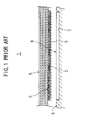
- Fig. 1 is a cross-sectional diagram showing a contactor 1 for a semiconductor device (hereinafter referred to as a contactor) of the related art.
- the contactor 1 includes a wiring substrate 2, an anisotropic conductive sheet 4, a multilayer substrate 5, and a base member 6.
- the wiring substrate 2 includes a base film made of resin and a wiring pattern formed thereon. Also, a part of the wiring pattern is provided with contact electrodes 3 to which terminals of a semiconductor device 8 (in the Figure, a wafer is illustrated as an example of the semiconductor device) are connected.
- the contact electrodes 3 extend to an upper surface (i.e., a surface opposite a surface provided with the contact electrodes 3) of the wiring substrate 2 via through holes or vias (not shown) formed in the base film.
- the multilayer substrate 5 is a multilayer wiring printed-circuit board, which includes a substrate made of glass-epoxy whereon a plurality of wiring substrate layers provided with wiring patterns are laminated. Also, the layers provided with the wiring patterns are each electrically connected by elements such as through holes. Therefore, in the related art, the multilayer substrate 5 is made of an extremely hard material (or a material with a high rigidity).
- the anisotropic conductive sheet 4 is provided between the wiring substrate 2 and the multilayer substrate 5.
- the anisotropic conductive sheet 4 is elastic and is conductive in a vertical direction in the Figure, so that an electric connection is established only at only at locations under pressure.
- the wiring substrate 2 is provided directly on the multilayer substrate 5 with high rigidity, it is not possible to overcome the variation of the heights of the terminals of the semiconductor device 8 or the contact electrodes 3 of the wiring substrate 2.
- the purpose of using the anisotropic conductive sheet 4 is to avoid such a drawback and thus positively connect the contact electrodes 3 to the plurality of terminals.
- the wiring substrate 2, the anisotropic conductive sheet 4 and the multilayer substrate 5 constitute an integrated body.
- the base member 6 is provided with a mounting portion 7 having a recessed shape corresponding to the contour of the semiconductor device 8.
- the semiconductor device 8 is mounted in the mounting portion 7 so as to be maintained by the base member 6.
- the semiconductor device 8 For electrically connecting the contactor 1 of the above structure and the semiconductor device 8, the semiconductor device 8 is mounted on the mounting portion 7 of the base member 6. Then, the wiring substrate 2 is pressed onto the semiconductor device 8. Thus, the contact electrodes 3 and the terminals of the semiconductor device 8 are connected and it is possible to establish an electrical conduction between the wiring substrate 2 and the semiconductor device 8.
- the contactor 1 includes the anisotropic conductive sheet 4 provided between the wiring substrate 2 and the multilayer substrate 5.
- another example of the contactor of the related art may include an anisotropic conductive sheet provided between a wiring substrate and a semiconductor device.
- a contactor with greater contact pressure between the wiring substrate and the semiconductor device. This is achieved by providing a seal member between a base member on which the semiconductor device wafer is mounted and the wiring substrate. A negative pressure is built up in an area sealed with the sealing member so that the wiring substrate will be pressed against the semiconductor wafer under atmospheric pressure.
- the other force is a pressure required for maintaining the wiring substrate 2 in position with the base member 6. This force is hereinafter referred to as a position maintaining force.
- the contact pressure should be adjusted for providing a good electrical connection between the contact electrodes 3 of the wiring substrate 2 and the terminals of the semiconductor device 8, thus preventing any deformation of the contact electrodes 3 and the terminals.
- the position maintaining force should be adjusted to a value sufficient for preventing any offset of the positioning of the wiring substrate 2 and the base member 6 when there is a certain external force being applied.
- the contact pressure and the position maintaining force cannot be adjusted independently.
- the wiring substrate and the semiconductor devices may be electrically connected by the above-described negative pressure. Then, if the negative pressure is released in order to release the contact pressure, the position maintaining force is also released. Accordingly, there is a drawback that the wiring substrate and the semiconductor devices are offset from the predetermined positions.
- the contact pressure and the position maintaining force are the same force.
- the contact pressure will also be increased, thus creating a risk of the terminals of the semiconductor device being seriously damaged.
- the flexibility of the wiring substrate 2 is provided by the elasticity of the anisotropic conductive sheet 4 and thus is limited to such elasticity. Therefore, it is not possible to compensate for any variation of heights of the contact electrodes 3 and the terminals which variation exceeds the elasticity of the anisotropic conductive sheet 4. Accordingly, when there is any variation of the heights of the fine-pitched terminals, the contact electrodes 3 cannot be connected to all of the terminals of the semiconductor device 8.
- a semiconductor device contactor includes a base unit for holding a semiconductor device provided with a plurality of terminals and a wiring substrate provided with contact electrodes at positions corresponding to at least some of the terminals.
- the contact electrodes and the terminals are electrically connected when the wiring substrate is held on the base unit.
- the semiconductor device contactor further includes: a position maintaining force applying mechanism for applying a position maintaining force between the base unit and the wiring substrate; and a contact pressure applying mechanism for applying a contact pressure between the semiconductor device and the wiring substrate.
- the position maintaining force applying mechanism and the contact pressure applying mechanism are operable in an independent manner.
- the testing device includes a semiconductor device contactor as described above and a chamber for accommodating the semiconductor device contactor.
- the chamber is constructed such that its internal atmosphere may be of a positive pressure.
- the contact pressure resulting from the negative pressure can be relatively increased by applying a high pressure in an atmosphere of the chamber.
- a stable contact pressure can be obtained.
- the testing method includes the steps of:
- an accurate positioning can be achieved by the steps a) and b). Also, a secure connection of the contact electrodes to the terminals can be achieved since, after positioning, first, the wiring substrate and the base unit are fixed by means of the position maintaining force applying mechanism and, then, the contact pressure is applied between the wiring substrate and the semiconductor device by means of the contact pressure applying mechanism.
- a method of cleaning a contactor for semiconductor devices includes the steps of:
- Fig. 1 is a cross-sectional diagram showing a contactor of the related art.
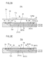
- Figs. 2A to 2C are cross-sectional diagrams showing a contactor of a first embodiment of the present invention taken along line I-I in Fig. 3.
- Fig. 3 is a plan view showing a base unit constituting the contactor of the first embodiment of the present invention.
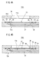
- Figs. 4A and 4B are cross-sectional diagrams showing a contactor of a second embodiment of the present invention.
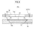
- Fig. 5 is a cross-sectional diagram showing a contactor of a third embodiment of the present invention.
- Fig. 6 is a cross-sectional diagram showing a contactor of a fourth embodiment of the present invention.
- Figs. 7A and 7B are cross-sectional diagrams showing a contactor of a fifth embodiment of the present invention.
- Figs. 8A and 8B are a plan view and a cross-sectional diagram, respectively, showing a contactor of a sixth embodiment of the present invention.
- Figs. 9A and 9B are cross-sectional diagrams showing a contactor of a seventh embodiment of the present invention.
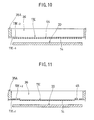
- Fig. 10 is a cross-sectional diagram showing a contactor of an eighth embodiment of the present invention.
- Fig. 11 is a cross-sectional diagram showing a contactor of a ninth embodiment of the present invention.
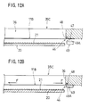
- Figs. 12A and 12B are cross-sectional diagrams showing a contactor of a tenth embodiment of the present invention.
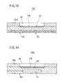
- Fig. 13 is a cross-sectional diagram showing a contactor of an eleventh embodiment of the present invention.
- Fig. 14 is a cross-sectional diagram showing a contactor of a twelfth embodiment of the present invention.
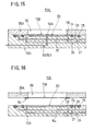
- Fig. 15 is a cross-sectional diagram showing a contactor of a thirteenth embodiment of the present invention.
- Fig. 16 is a cross-sectional diagram showing a contactor of a fourteenth embodiment of the present invention.
- Fig. 17 is a cross-sectional diagram showing a contactor of a fifteenth embodiment of the present invention.
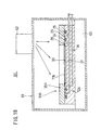
- Fig. 18 is a cross-sectional diagram showing a contactor of a sixteenth embodiment of the present invention.
- Fig. 19 is a cross-sectional diagram showing a testing apparatus of one embodiment of the present invention, the testing apparatus utilizing a contactor.
- Fig. 20 is a cross-sectional diagram showing a testing apparatus utilizing the contactor of the first embodiment of the present invention.
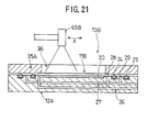
- Fig. 21 is a cross-sectional diagram showing a testing apparatus utilizing the contactor of the second embodiment of the present invention.
- Fig. 22 is a cleaning method of semiconductor device contactor of one embodiment of the present invention.
- Figs. 2A to 2C and Fig. 3 are cross-sectional diagrams showing a semiconductor device contactor 10A (the semiconductor device contactor is hereinafter simply referred to as a contactor) of a first embodiment of the present invention.
- contactors 10A to 10I of the embodiments described later may be applied to any types of semiconductor chip and semiconductor device (hereinafter both are generically referred to as a semiconductor device) such as a wafer, a bare-chip, BGA (Ball Grid Array), an SOP (Small Outline Package) and a QFP (Quad Flat Package).
- a semiconductor device 20 is described as a wafer.
- the contactor 10A generally includes a wiring substrate 11A and a base unit 12A.
- the wiring substrate 11A includes a wiring pattern, not shown, provided on a base film 13.
- the base film 13 is, for example, made of a resin such as polyimide (PI) and has a thickness of about 25 to 100 pm.
- the wiring pattern is made of an electrically conductive material such as a copper foil or an aluminum foil patterned into a predetermined configuration. Also, the wiring pattern is provided with contact electrodes 14 which may be electrically connected to terminals 21 provided on the semiconductor device 20 (see Figs. 9A and 9B).
- the wiring substrate 11A is configured such that a region in which the contact electrodes 14 will be connected to the terminals 21 of the semiconductor device 20 is flexible. Hereinafter, this region will be referred to as a connection region 18. In order to give flexibility to the connection region 18, the thickness of the base film 13 may be reduced at a corresponding area. Also, the wiring substrate 11A is given a predetermined rigidity at a peripheral area of the connection region 18.
- the base unit 12A may be made of metal, such as aluminum and stainless steel, or of hard resin.
- the base unit 12A is provided with a recessed mounting part 15 in which the semiconductor device 20 can be mounted.
- the base unit 12A is further provided with a contact pressure applying mechanism 16 and a position maintaining force applying mechanism 17.
- the contact pressure applying mechanism 16 generally includes a first seal member 24 and a first suction pipe 26.
- the first seal member 24 may be an O-ring. As shown in Fig. 3, the first seal member 24 is provided on the base unit 12A and surrounds the semiconductor device 20 mounted on the mounting part 15. In detail, the first seal member 24 is provided in a first recessed part 22 which is formed in the base unit 12A and surrounds the mounting part 15.
- the first seal member 24 is provided in such a manner that it slightly protrudes from the top surface of the base unit 12A. Therefore, as shown in Figs. 2B and 2C, when the wiring substrate 11A is mounted on the base unit 12A, the first seal member 24 touches the wiring pattern 11A in a hermetic manner.
- the wiring substrate 11A when the wiring substrate 11A is mounted on the base unit 12A, the wiring substrate 11A, the base unit 12A and the first seal member 24 enclose a sealed spatial region.
- the sealed spatial region will be referred to as a first closed region 31.
- the area of the first closed region 31 is provided so as to cover at least the above-described connection region 18.
- the first suction pipe 26 is provided inside the base unit 12A.
- One end of the first suction pipe 26 opens at a position between the mounting part 15 and the first seal member 24.
- the first suction pipe 26 opens on a surface on which the semiconductor device 20 is mounted.
- this opening will be referred to as a contact pressure opening 28. Therefore, the contact pressure opening 28 opens in the first closed region 31.
- four contact pressure openings 28 are provided in the first closed region 31.
- the other end of the first suction pipe 26 extends at a side surface of the base unit 12A and is connected to a first vacuum device which is not shown in the Figure. Therefore, by driving the first vacuum device, the first closed region 31 is vacuumed via the first suction pipe 26. Thus, a negative pressure is built up in the first closed region 31.
- a communication stepped portion 30 is formed at a peripheral position of the mounting part 15.
- the communication stepped portion 30 is slightly recessed from the upper surface of the base unit 12A.
- the mounting part 15 is also included in the first closed region 31 and a negative pressure is applied inside the mounting part 15. Further, the negative pressure within the first closed region 31 and the mounting part 15 can be adjusted to any value by controlling the first vacuum device.
- the first closed region 31 covers the connection region 18.
- the first vacuum device is driven with the wiring substrate 11A being mounted on the first seal member 24, the first closed region 31 will be brought to a negative pressure.
- the connection region 18 of the wiring substrate 11A will be pressed towards the semiconductor device 20. Therefore, the contact electrodes 14 of the wiring substrate 11A can be pressed to the terminals 21 of the semiconductor device 20.
- the negative pressure applied by the contact pressure applying mechanism 16 serves as a contact pressure for pressing the contact electrodes 14 of the wiring substrate 11A to the terminals 21 of the semiconductor device 20.
- the contact pressure can be adjusted to any value by controlling the first vacuum device.
- the contact pressure may be controlled by a structure in which a number and radius of the contact pressure openings 28 can be adjusted.
- the position maintaining force applying mechanism 17 of the present embodiment generally includes a second seal member 25 and a second suction pipe 27.
- the second seal member 25 may be an O-ring. As shown in Fig. 3, the second seal member 25 is provided on the base unit 12A and surrounds the first seal member 24. In detail, the second seal member 25 is provided in a second recessed part 23 which is formed in the base unit 12A and surrounding the first seal member 24.
- the second seal member 25 is provided in such a manner that it slightly protrudes from the top surface of the base unit 12A.
- the second seal member 25 is protruded substantially by an equal amount to that of the first seal member 24. Therefore, as shown in Figs. 2B and 2C, when the wiring substrate 11A is mounted on the base unit 12A, the first and second seal members 24, 25 contact the wiring pattern 11A in a hermetic manner.
- a sealed spatial region is created by the wiring substrate 11A, the base unit 12A, the first seal member 24 and the second seal member 25.
- the sealed spatial region will be referred to as a second closed region 32.
- the second closed region 32 is a completely independent region since it is hermetically separated from the first closed region 31 by means of the first seal member 24.
- a second suction pipe 27 is provided inside the base unit 12A.
- One end of the second suction pipe 27 opens at a position between the first seal member 24 and the second seal member 25.
- this opening will be referred to as a position maintaining force opening 29. Therefore, the position maintaining force opening 29 opens in the second closed region 32.
- eight position maintaining force openings 29 are provided in the second closed region 32.
- the other end of the second suction pipe 27 extends at a side surface of the base unit 12A and is connected to a second vacuum device which is not shown in the Figure. Therefore, by driving the second vacuum device, the second closed region 32 is vacuumed via the second suction pipe 27. Thus, a negative pressure is built up in the second closed region 32.
- the first and second vacuum devices may be integrated as a single device, but it is necessary that the first suction pipe 26 and the second suction pipe 27 can be independently adjusted to their respective degrees of vacuum.
- the second vacuum device when the second vacuum device is driven with the wiring substrate 11A being mounted on the first and second seal members 24, 25, the second closed region 32 will be brought to a negative pressure.
- the wiring substrate 11A will be pressed towards the base unit 12A. Therefore, the wiring substrate 11A can be held (fixed) on the base unit 12A.
- the negative pressure applied by the position maintaining force applying mechanism 17 serves as a contact pressure for fixedly holding the wiring substrate 11A on the base unit 12A.
- the position maintaining force can be adjusted to any value by controlling the second vacuum device.
- the first and second closed regions 31, 32 are hermetically defined as describe above, it is possible to independently adjust the contact pressure applied in the first closed region 31 and the position maintaining force applied in the second closed region 32.
- the contact pressure may be controlled by a structure in which a number and radius of the position maintaining force openings 29 can be adjusted.
- the semiconductor device 20 is mounted on the mounting part 15 of the base unit 12A. Then, the wiring substrate 11A is placed on the base unit 12A in such a manner that the wiring substrate 11A is positioned against the semiconductor device 20. In this state, the first and second seal members 24, 25 are in contact with the wiring substrate 11A.
- the second vacuum device is driven so as to generate the position maintaining force (negative pressure) in the second closed region 32.
- the position maintaining force is adjusted to a value sufficient for securely holding the wiring substrate 11A on the base unit 12A.
- the wiring substrate 11A can be securely held on the base unit 12A. However, there is no contact pressure (negative pressure) applied to the first closed region 31. Also, since the first closed region 31 is completely independent of the second closed region 32, the connection region 18 of the wiring substrate 11A will be separated from the semiconductor device 20.
- the first vacuum device is driven so as to generate the contact pressure (negative pressure) in the first closed region 31.
- the contact pressure is adjusted to a value suitable for connecting the contact electrodes 14 and the terminals 21.
- a good connecting state may be achieved between the contact electrodes 14 and the terminals 21.
- the contact electrodes 14 and the terminals 21 will not be damaged during the connecting process.
- connection region 18 having the contact electrodes 14 has greater flexibility than other parts. Therefore, when the contact pressure is applied, the connection region 18 will be uniformly connected to all of the terminals 21 of the semiconductor device 20. Therefore, even if, as in the present embodiment, the wafer is used as the semiconductor device 20 and thus there are a large number of terminals, the contact electrodes 14 of the wiring substrate 11A can be positively connected to all of the terminals 21, respectively.
- the contact pressure applying mechanism 16 and the position maintaining force applying mechanism 17 are provided independently. Note that the contact pressure applying mechanism 16 produces the contact pressure between the semiconductor device 20 and the wiring substrate 11A, and the position maintaining force applying mechanism 17 produces the position maintaining force between the base unit 12A and the wiring substrate 11A. Therefore, the position maintaining force and the contact pressure can be controlled (operated) independently.
- the contact pressure and the position maintaining force are prevented from influencing each other. Therefore, the optimal position maintaining force for holding the wiring substrate 11A on the base unit 12A and the optimal contact pressure for connecting the semiconductor device 20 to the wiring substrate 11A can be generated independently. Thus, it is possible to achieve the accurate positioning between the wiring substrate 11A and the base unit 12A. Also, it is possible to keep the semiconductor device 20 and the wiring substrate 11A in a secure and stable contact state.
- the negative pressure is used as the contact pressure between the semiconductor device 20 and the wiring substrate 11A. Therefore, the wiring substrate 11A can be uniformly connected to the semiconductor device 20. That is to say, the contact pressure (i.e., negative pressure) in the first closed region 31 is uniformly applied to the inner wall of the first closed region 31.
- the wiring substrate 11A can be uniformly connected to the semiconductor device 20. Therefore, even if the semiconductor device 20 is provided with a larger number of terminals, all of the terminals 21 can be securely connected to the contact electrodes 14, respectively.
- the negative pressure is also used as the position maintaining force, so that the position maintaining force (negative pressure) is uniformly applied to the entire inner surface of the second closed region 32. Therefore, the wiring substrate 11A can be held on the base unit 12A with the uniform position maintaining force. Therefore, the wiring substrate 11A can be prevented from being tilted during mounting, and this can also achieve a stable contact state.
- a single wafer is used as the semiconductor device 20.
- a plurality of the above-described semiconductor devices are mounted on the mounting part 15 and the wiring substrate is totally and simultaneously connected to the plurality of the semiconductor devices.
- the semiconductor device 20 is tested with such a structure, it is possible to improve a testing efficiency.
- Figs. 4A and 4B are cross-sectional diagrams showing a contactor 10B related to the second embodiment of the present invention.
- the same structures as those described for the contactor 10A of the first embodiment in Figs. 2A to 2C and Fig. 3 will be indicated with the same reference numerals and detailed a description thereof will be omitted. This also applies to each of the embodiments described below.
- the wiring substrate 11A is directly mounted (by suction force) on the base unit 12A.
- the contactor 10B of the second embodiment is characterized in that there is provided a cover unit 35A for holding the wiring substrate 11B.
- the cover unit 35A is made of the same material as that of the base unit 12A. Also, a cover unit opening 36 is provided in the central part of the base unit 12A at an area corresponding to the connection region 18 of the wiring substrate 11B.
- the wiring substrate 11B of the present embodiment differs from the wiring substrate 11A used in the first embodiment in that the wiring substrate 11B is entirely flexible.
- the wiring substrate 11B has an entirely uniform structure, it is possible to reduce the cost as compared to the wiring substrate 11A.
- the wiring substrate 11B is fixed on the lower surface (the surface opposing the base unit 12A) of the cover unit 35A by, for example, an adhesive agent.
- the wiring substrate 11B When it is attempted to mount the entire flexible wiring substrate 11B on the base unit 12A without using the cover unit 35A, the wiring substrate 11B will be considerably deformed due to a great position maintaining force particularly at the second closed region 32. Accordingly, the connection region 18 will also be deformed so that it is not possible to achieve a good connection. For this reason, the wiring substrate 11A used in the first embodiment is configured such that the peripheral part of the connection region 18 is rigid.
- the entire flexible wiring substrate 11B is provided on the cover unit 35A. Therefore, it is possible to connect the wiring substrate 11B to the semiconductor device 20 with a predetermined contact pressure. Also, since the cover unit 35A is provided with the cover unit opening 36 at a position opposing the connection region 18, the wiring substrate 11B remains flexible in the connection region 18.
- the contact electrode 14 of the wiring substrate 11B can be positively connected to all of the terminals 21 of the semiconductor device 20. Further, as shown in Fig. 4B, the second closed region 32, in which the position maintaining force is applied, opposes the lower surface of the cover unit 35A. Therefore, even if the position maintaining force is increased, there will be no deformation produced in the wiring substrate 11B. Therefore, the wiring substrate 11B can be positively held on the base unit 12A.
- Fig. 5 is a cross-sectional diagram showing the contactor 10C of the third embodiment.
- a negative pressure is used for the position maintaining force applying mechanism 17.
- the contactor 10C of the third embodiment is characterized in that a fastening mechanism is used for the position maintaining force applying mechanism 17.
- the fastening mechanism is defined as a mechanism for holding the wiring substrate on the base unit by means of a mechanically produced force.
- the fastening mechanism is realized by screws 37. These screws will be hereinafter referred to as position maintaining force applying screws.
- the position maintaining force applying screw 37 is penetrated through a through hole provided in the cover unit 35B.
- the base unit 12B is provided with screw holes in which the position maintaining force applying screws 37 may be screwed.
- the cover unit 35B is mounted on the base unit 12B with the wiring substrate 11B being positioned with the semiconductor device 20, and the position maintaining force applying screw 37 is fastened.
- the cover unit 35B (the wiring substrate 11B) will be held on the base unit 12B.
- the position maintaining force can be adjusted by fastening the position maintaining force applying screw 37.
- a fastening force produced by the position maintaining force applying screws 37 serves as the position maintaining force between the wiring substrate 11B and the base unit 12B.
- the position maintaining force applying mechanism 17 of a comparatively simple and cost effective structure can be achieved.
- Fig. 6 is a cross-sectional diagram showing the contactor 10D of the fourth embodiment of the present invention.
- the present embodiment is characterized in that the position maintaining force applying mechanisms of the first and second embodiments using the negative pressure and that of the third embodiment using a fastening mechanism are combined.
- the position maintaining force applying mechanisms of the first and second embodiments using the negative pressure and that of the third embodiment using a fastening mechanism may be appropriately combined. It is not necessary to provide the position maintaining force applying mechanisms individually.
- Figs. 7A and 7B are cross-sectional diagrams showing the contactor 10E of the fifth embodiment.
- the contactor 10E of the present embodiment is characterized in that the contact pressure applying mechanism 16 is used as a lifting mechanism.
- the lifting mechanism is defined as a mechanism for applying a contact pressure by moving the semiconductor unit 20 mounted on the mounting part 15 towards the wiring substrate 11B.
- the lifting mechanism is realized by a lifting element 38 such as a piezoelectric element whose thickness may be electrically altered.
- the lifting element 38 is provided at the lower part of the mounting part 15 of the base unit 12D. Thus, when the voltage is applied to the lifting element 38, the semiconductor device 20 place on the lifting element 38 will move upwards. Also, by ceasing the voltage application, the semiconductor device 20 will move downwards.
- the position maintaining force applying mechanism 17 includes the first and second seal member 24, 25, the second suction pipe 27, and the position maintaining force opening 29.
- the contact pressure can be applied between the semiconductor device 20 and the wiring substrate 11B by means of the lifting element 38 (lifting mechanism). Also, by using the contact pressure applying mechanism 16 as the lifting mechanism as in the present embodiment, it is possible to produce the contact pressure between the semiconductor device 20 and the wiring substrate 11B with a comparatively simple structure. Note that the contact pressure can be adjusted by controlling the voltage applied to the lifting element 38.
- Figs. 8A and 8B are diagrams showing a wiring substrate 11C provided on the contactor of the sixth embodiment.
- Fig. 8A is a flat enlarged diagram showing a neighborhood of the cover unit opening 36 of the cover unit 35A on which the wiring substrate 11C is provided.
- Fig. 8A is a cross-sectional diagram showing the cover unit 35A on which the wiring substrate 11C is provided.
- the present embodiment is characterized in that a deformable part 40 is provided at a peripheral part of the connection region 18 of the wiring substrate 11C.
- the connection region 18 is a region in which the contact electrodes 14 are connected to the terminals 21 of the semiconductor device 20.
- the deformable part 40 is constructed by a plurality of small holes 41 provided along the periphery of the connection region 18.
- the small holes 41 may be formed by various methods including etching, punching, and laser processing.
- a back-up sheet 39A is provided on the back surface of the wiring substrate 11C.
- the peripheral part of the wiring substrate 11C will be more flexible.
- the position of the deformable part 40 is not limited to the peripheral part of the connection region 18, but may also be at the position opposing the region in which the terminals 21 of the semiconductor device 20 are not formed.
- the deformable part 40 is not limited to a structure using the small holes 41, but can be achieved by reducing the thickness of the base film 13 by, for example, etching.
- Figs. 9A and 9B are enlarged cross-sectional diagrams showing a wiring substrate 11D provided on the contactor of the seventh embodiment.
- Fig. 9A is an enlarged diagram showing a neighboring part of the cover unit opening 36 of the cover unit 35A on which the wiring substrate 11D is provided.
- Fig. 9B is an enlarged diagram showing the wiring substrate 11D being in a connected state with the terminals 21 of the semiconductor device 20.
- the wiring substrate 11D includes a plurality of laminated wiring layers.
- two wiring layers 42A, 42B are illustrated.
- the wiring layers 42A, 42B are provided with contact electrodes 14A, 14B which are selectively connected to the terminals 21 of the semiconductor device 20.
- the contact electrodes 14A, 14B are provided on respective base films 13A, 13B.
- the terminals 21 of the semiconductor device 20 are configured as bumps.
- the wiring substrate 11D is provided with insert holes 43 provided at predetermined positions to be connected to the terminals 21 of the semiconductor device 20.
- the contact electrodes 14A, 14B to be connected to the terminals 21 corresponding to the insert hole positions are provided so as to extend in the insert holes 43. Therefore, when the wiring substrate 11D is electrically connected to the semiconductor device 20, the terminals 21 made of bumps will be inserted in the insert holes 43. Thereby the terminals 21 will be connected to the predetermined contact electrodes 14A, 14B, thus achieving an electrical conduction.
- an increased number of contact electrodes 14A, 14b can be provided compared to a single layered wiring substrate. Therefore, the contactor can still be used with the high-density semiconductor device 20 having an increased number of terminals.
- Fig. 10 is an enlarged cross-sectional diagram showing a wiring substrate 11E provided on the contactor of the eighth embodiment.
- the wiring substrate 11E is provided with through holes 44 serving as conducting parts.
- the surface of the wiring substrate 11E on which the semiconductor is connected will be referred to as a connecting surface 11E-1.
- the surface opposite to the connecting surface 11E-1 will be referred to as an opposite surface 11E-2.
- the present embodiment is characterized in that the connecting surface 11E-1 and the opposite surface 11E-2 are electrically connected by the through holes 44.
- Fig. 11 is an enlarged cross-sectional diagram showing the wiring substrate 11E provided on the contactor of the ninth embodiment.
- the present embodiment is characterized in that the wiring substrate 11E used in the eight embodiment is utilized together with electronic components 45 mounted on the opposite surface 11E-2.
- the electronic components 45 may be elements such as a capacitor, a resistor, a fuse, and a self burn-in circuit.
- the wiring substrate itself has a function of implementing a test on the semiconductor device 20.
- Figs. 12A and 12B are enlarged cross-sectional diagrams showing the wiring substrate 11B provided on the contactor of the tenth embodiment.
- the present embodiment is characterized in that a tension applying mechanism 46 is provided for applying a predetermined tension F on the wiring substrate 11B.
- the tension applying mechanism 46 includes a tapered surface 47, an accommodation recess 48 and a protruded component 49.
- the tapered surface 47 is provided on the surface of the cover unit 35C opposing the base unit 12A (not shown in Figs. 12A and 12B).
- the accommodation recess 48 is formed at a part of the tapered surface 47.
- the protruded component 49 has a protrusion 49A to be fitted into the accommodation recess 48.
- Fig. 13 is a cross-sectional diagram showing the contactor 10F of the eleventh embodiment.
- the contact pressure applying mechanism 16 and the position maintaining force applying mechanism 17 are omitted from the figure.
- the present embodiment is characterized in that a base unit 12E has a heat dissipation function.
- the base unit 12E is made of a material with good thermal conductivity and is provided with a heat dissipation fin part 50.
- Fig. 14 is a cross-sectional diagram showing the contactor 10G of the twelfth embodiment.
- the contact pressure applying mechanism 16 and the position maintaining force applying mechanism 17 are omitted from the figure.
- the present embodiment is characterized in that a base unit 12G is provided with a temperature controlling device 51.
- the temperature controlling device 51 internally includes at least one of a temperature applying mechanism, a heat absorption mechanism and a temperature detecting mechanism.
- the temperature of the semiconductor device 20 during the test can be adjusted to a proper temperature. Also, it is possible to adjust any positioning offset due to thermal expansion of the base unit 12E.
- the temperature applying mechanism may be an electric heater and the heat absorption mechanism may be, for example, a Peltier element.
- Fig. 15 is a cross-sectional diagram showing the contactor 10H of the thirteenth embodiment.
- the contactor 10H of the present embodiment is characterized in that a base unit 12G is provided with a holding mechanism 52 for forcing the semiconductor device 20 to be held on the mounting part 15.
- the holding mechanism 52 is formed by a holding suction pipe 53 provided in the base unit 12G.
- One end of the holding suction pipe 53 opens in the mounting part 15.
- the opening will be referred to as a semiconductor device holding opening 53A.
- the other end of the holding suction pipe 53 is pulled out at a side surface of the base unit 12G and is connected to a third vacuum device which is not shown in the Figure.
- the semiconductor device 20 mounted on the mounting part 15 is vacuumed at the semiconductor device holding opening 53A.
- the semiconductor device 20 is held on the base unit 12G.
- the semiconductor device 20 can be fixed to the base unit 12G before positioning the wiring substrate 11B (cover unit 35A) and the base unit 12G. Thereafter, the semiconductor device 20 is prevented from being displaced in the mounting part 15, so that the positioning can be achieved with a higher accuracy. (Note that there a small gap between the mounting part 15 and the semiconductor device 20 for facilitating the attachment and removal of the semiconductor device 20.)
- the wafer when used as the semiconductor device 20, there may be a warp in the wafer.
- a plurality of the semiconductor device holding openings 53A can be formed in the mounting part.
- the back surface of the mounted wafer may be entirely and uniformly vacuumed so as to correct the warp of the wafer (semiconductor device 20).
- Fig. 16 is a cross-sectional diagram showing the contactor 10I of the fourteenth embodiment.
- the contactor 10I of the present embodiment is characterized in that at least one of the wiring substrate 11B, the cover unit 35A, and the base unit 12A is provided with a friction increasing part for increasing the friction produced between the wiring substrate 11B (cover unit 35A) and the base unit 12A.
- the friction increasing part is a friction increasing sheet 54 having a comparatively high friction coefficient (e.g., rubber) at the surface. Also, the friction increasing sheet 54 is provided around the wiring substrate 11B.
- the friction increasing sheet 54 serves as the friction increasing part.
- the friction increasing part is not limited but can be made by directly forming a coarse surface on the cover unit and the base unit.
- Fig. 17 is an enlarged diagram showing a neighborhood of the wiring substrate 11B provided on the contactor of the fifteen the embodiment.
- the contactor 10I of the present invention is provided with a third seal member 55 between the wiring substrate 11A and the cover unit 35A and a forth seal member 56 provided in a base unit 12H.
- a third seal member 55 between the wiring substrate 11A and the cover unit 35A
- a forth seal member 56 provided in a base unit 12H.
- the third seal member 55 is a sheet-like seal member, and can be made of a resin of such as a silicon type or a fluorine type.
- the forth seal member 56 is for example sphere-like and can be made of a resin of such as the silicon type or the fluorine type.
- the forth seal member 56 is provided in the contact pressure opening 28 of the first suction pipe 26.
- the contact pressure opening 28 communicates with the mounting part 15 via the communication stepped part 30. Therefore, when applying the contact pressure in the first closed region 31, the fourth seal member 56 will not be obstructive.
- the contact pressure can be positively produced in the first closed region 31, so that the wiring substrate 11B can be securely connected to the semiconductor device 20.
- Fig. 18 is an enlarged diagram showing a neighborhood of the wiring substrate 11B provided on the contactor of the sixteenth embodiment.
- the present embodiment is characterized in that a back-up sheet 39B having protrusions and recesses is provided on the opposite surface of the wiring substrate 11B (the surface opposite to the surface connected to the semiconductor device 20).
- the back-up sheet 39B is made of an elastic material such as silicon rubber and is provided with protrusions at positions opposing the contact electrodes 14. With the back-up sheet 39B having a certain elasticity, any variation between the heights of the terminals 21 of the semiconductor device 20 or the contact electrodes 14 of the wiring substrate 11B will be compensated for by a deformation of the back-up sheet 39B. Also, the back-up sheet 39B will produce an elastic restoration force by being pressed with the terminals 21. Therefore, this elastic restoration force serves as the contact pressure. Thus, in the present embodiment, since the contact pressure is also produced in the back-up sheet 39B, it is possible to implement a more stable connection.
- FIG. 19 is schematic diagram of a testing apparatus 60 of an embodiment of the present invention.
- the testing apparatus 60 includes the contactor 10B, a testing apparatus chamber 61 and a compressed air producing device 62.
- the contactor 10B is the contactor of the second embodiment described above by reference to Fig. 4.
- the contactor available for the testing apparatus 60 is not limited to the contactor 10B of the second embodiment, but can be any one of the contactors described above.
- the testing apparatus chamber 61 is an airtight container and the contactor 10B is installed therein. With the contactor 10B being installed in the testing apparatus chamber 61, the first and second suction pipe 26, 27 extend outside the testing apparatus 60 and are connected to the first and second vacuum devices. In the figure, the contactor 10B is mounted on a base table 63.
- the compressed air producing device 62 includes a compression pump, and can introduce compressed air into the testing apparatus chamber 61. Therefore, by driving the compression air-producing device 62, the pressure within the testing apparatus chamber 61 will become a positive pressure.
- the testing apparatus 60 of the present embodiment includes the testing apparatus chamber 61 having an internal atmosphere brought to a positive pressure by the compressed air producing device 62 provided thereon and the contactor 10B installed in the testing apparatus chamber 61. Therefore, it is possible to securely connect the contact electrodes 14 to the terminals 21 even when the contact pressure due to the negative pressure produced in the first closed region 31 is insufficient.
- the positive pressure when the positive pressure is produced in the testing apparatus chamber 61 by means of the compressed air generating device 62, this positive pressure causes a relatively great positive pressure produced in the first closed region 31.
- the contact pressure is determined by an atmospheric pressure external to the first closed region 31 and the negative pressure generated by the first vacuum device. Therefore, as the atmosphere in the testing apparatus chamber 61 is brought to a higher pressure, the contact pressure will increase relatively. Thus, it is possible to obtain the contact pressure sufficient for connecting the contact electrodes 14 to the terminals 21 of the semiconductor device 20.
- a testing method using the contactor of the first embodiment of the present invention will be described.
- the method of testing the semiconductor device 20 using the contactor 10B of the second embodiment illustrated in Figs. 4A and 4B will be described.
- the method of the present invention is not limited to the contactor 10B of the second embodiment, but any one of the contactors of the above embodiments can be used.
- the semiconductor device 20 is mounted on the mounting part 15 of the base unit 12A. Then, as shown in Fig. 20, a position recognition process of the terminals 21 of the semiconductor device 20 and the contact electrodes 14 of the wiring substrate 11B is implemented by means of a CCD camera 65A. Here, the terminals 21 and the contact electrodes 14 are not shown in the figure.
- the CCD camera 65A of the present embodiment is capable of imaging both directions in its upper and lower side. Therefore, since the recognition process of the terminals 21 and the contact electrodes 14 can be implemented simultaneously, the time required for the recognition process is reduced.
- a position offset between the terminals 21 and the contact electrodes 14 is detected and a position correction value is computed from the detected position offsets.
- the positioning of the wiring substrate 11B and the base unit 12A is implemented.
- the position maintaining force applying mechanism 17 is driven so as to produce a negative pressure in the second closed region 32.
- the position maintaining force is produced between the wiring substrate 11B (cover unit 35A) and the base unit 12A.
- the wiring substrate 11 and the semiconductor device 20 will be maintained in a positioned state.
- the contact pressure applying mechanism 16 is driven so as to produce a negative pressure in the first closed region 31.
- the contact pressure is applied between the wiring substrate 11B and the semiconductor device 20.
- the wiring substrate 11B will be connected to the semiconductor device 20 so that the predetermined test can be implemented.
- the position recognition process of the terminals 21 of the semiconductor device 20 and the contact electrodes 14 is implemented. Then, the wiring substrate 11B and the semiconductor device 20 (base unit 12A) are positioned based on the position correction value obtained from the position recognition process. Thus, according to the testing method of the present embodiment, the positioning can be implemented with a comparatively high accuracy.
- the position maintaining force applying mechanism 17 is driven so as to apply a position maintaining force between the wiring substrate 11B and the base unit 12A.
- the position maintaining force applying mechanism 17 is driven so as to apply a position maintaining force between the wiring substrate 11B and the base unit 12A.
- a CCD camera 65A which is capable of imaging both directions in its upper and lower side.
- the recognition process is implemented by moving this CCD camera 65A between the wiring substrate 11B and the semiconductor device 20.
- the CCD camera 65A which can image both directions in its upper and lower sides is expensive. Also, an operability is not particularly good when moving the CCD camera 65A between the wiring substrate 11B and the semiconductor device 20 during the recognition process.
- the present embodiment is characterized in that a CCD camera 65B is placed above the cover unit 35A.
- the semiconductor device 20 can be positioned by looking through the wiring substrate 11B from above.
- a transparent PI tape is used for the wiring substrate 11B such that the semiconductor device 20 can seen through the wiring substrate 11B.
- the CCD camera 65B can be of a simple and cheap structure capable of imaging only one direction, since there is not a need for vertical imaging as is required for the method of the first embodiment.
- a method of cleaning the contactor of one embodiment of the present invention will be described with reference to Fig. 22.
- the method of cleaning according to the present embodiment can be applied to any one of the contactors 10A to 10I of the above-described embodiments.
- the method of the present embodiment is for implementing a cleaning process of the contact electrodes 14 of the wiring substrates 11A to 11E provided on the respective contactors 10A to 10I.
- a method of implementing a cleaning process of the contactor 10B of the second embodiment will be described.
- a cleaning member 70 is mounted on the mounting part 15 provided in the base unit 12A.
- the cleaning member 70 may be a wrapping sheet with fine protrusions and recesses 71.
- the contact pressure applying mechanism 16 is repeatedly driven and stopped. Thereby, the first closed area 31 is alternately and repeatedly brought to a state in which the contact pressure is applied and a state in which the contact pressure is not applied. In other words, the wiring substrate 11A will vibrate in the direction indicated with an arrow H in the figure.
- the cleaning member 70 will be repeatedly in contact with, slide on or collide with the contact electrodes 14 provided on the wiring substrate 11B.
- unnecessary layers such as an oxidization layer disposed on the contact electrodes 14 can be removed by means of the cleaning member 70.
- the contact electrodes 14 can be always kept in a good state, and it is possible to improve the reliability of the electric connection of the wiring substrate 11B against the semiconductor device 20.
Landscapes
- Engineering & Computer Science (AREA)
- Computer Hardware Design (AREA)
- Microelectronics & Electronic Packaging (AREA)
- General Engineering & Computer Science (AREA)
- Physics & Mathematics (AREA)
- General Physics & Mathematics (AREA)
- Testing Of Individual Semiconductor Devices (AREA)
- Testing Or Measuring Of Semiconductors Or The Like (AREA)
- Measuring Leads Or Probes (AREA)
- Tests Of Electronic Circuits (AREA)
Applications Claiming Priority (2)
| Application Number | Priority Date | Filing Date | Title |
|---|---|---|---|
| JP36161898 | 1998-12-18 | ||
| JP10361618A JP2000180469A (ja) | 1998-12-18 | 1998-12-18 | 半導体装置用コンタクタ及び半導体装置用コンタクタを用いた試験装置及び半導体装置用コンタクタを用いた試験方法及び半導体装置用コンタクタのクリーニング方法 |
Publications (2)
| Publication Number | Publication Date |
|---|---|
| EP1011134A1 true EP1011134A1 (de) | 2000-06-21 |
| EP1011134B1 EP1011134B1 (de) | 2013-01-23 |
Family
ID=18474308
Family Applications (1)
| Application Number | Title | Priority Date | Filing Date |
|---|---|---|---|
| EP99306225A Expired - Lifetime EP1011134B1 (de) | 1998-12-18 | 1999-08-05 | Kontaktor für Halbleiterbauelemente, Testvorrichtung mit solchem Kontaktor, Testverfahren mit solchem Kontaktor und Reinigungsverfahren für solchen Kontaktor |
Country Status (6)
| Country | Link |
|---|---|
| US (3) | US6466046B1 (de) |
| EP (1) | EP1011134B1 (de) |
| JP (1) | JP2000180469A (de) |
| KR (1) | KR100550022B1 (de) |
| CN (1) | CN1322567C (de) |
| TW (1) | TW418480B (de) |
Cited By (2)
| Publication number | Priority date | Publication date | Assignee | Title |
|---|---|---|---|---|
| WO2003102604A1 (en) * | 2002-06-03 | 2003-12-11 | Koninklijke Philips Electronics N.V. | Device and method of testing an electronic component |
| EP2015087A1 (de) * | 2007-07-12 | 2009-01-14 | Multitest Elektronische Systeme Gmbh | Vorrichtung zum Testen von elektronischen Bauelementen, insbesondere IC's, mit innerhalb einer Drucktestkammer angeordnetem Abdichtboard |
Families Citing this family (54)
| Publication number | Priority date | Publication date | Assignee | Title |
|---|---|---|---|---|
| US5345170A (en) * | 1992-06-11 | 1994-09-06 | Cascade Microtech, Inc. | Wafer probe station having integrated guarding, Kelvin connection and shielding systems |
| US6380751B2 (en) | 1992-06-11 | 2002-04-30 | Cascade Microtech, Inc. | Wafer probe station having environment control enclosure |
| US6002263A (en) | 1997-06-06 | 1999-12-14 | Cascade Microtech, Inc. | Probe station having inner and outer shielding |
| JP2000180469A (ja) * | 1998-12-18 | 2000-06-30 | Fujitsu Ltd | 半導体装置用コンタクタ及び半導体装置用コンタクタを用いた試験装置及び半導体装置用コンタクタを用いた試験方法及び半導体装置用コンタクタのクリーニング方法 |
| US6445202B1 (en) * | 1999-06-30 | 2002-09-03 | Cascade Microtech, Inc. | Probe station thermal chuck with shielding for capacitive current |
| JP4592885B2 (ja) * | 2000-07-31 | 2010-12-08 | 富士通セミコンダクター株式会社 | 半導体基板試験装置 |
| US6965226B2 (en) * | 2000-09-05 | 2005-11-15 | Cascade Microtech, Inc. | Chuck for holding a device under test |
| US6914423B2 (en) | 2000-09-05 | 2005-07-05 | Cascade Microtech, Inc. | Probe station |
| WO2003020467A1 (en) * | 2001-08-31 | 2003-03-13 | Cascade Microtech, Inc. | Optical testing device |
| JP2003086610A (ja) * | 2001-09-10 | 2003-03-20 | Mitsubishi Electric Corp | 樹脂封止半導体装置およびその製造方法 |
| JP4173306B2 (ja) * | 2001-11-30 | 2008-10-29 | 東京エレクトロン株式会社 | 信頼性評価試験装置、信頼性評価試験システム及び信頼性評価試験方法 |
| DE10161755B4 (de) * | 2001-12-15 | 2005-12-15 | Infineon Technologies Ag | Kontaktstift zum Testen mikroelektronischer Bauteile mit kugelförmigen Kontakten |
| US7555013B2 (en) * | 2002-08-12 | 2009-06-30 | Harris Corporation | Method and system for the blind determination of frequency hopping system characteristics and synchronization thereto |
| US6847219B1 (en) | 2002-11-08 | 2005-01-25 | Cascade Microtech, Inc. | Probe station with low noise characteristics |
| US7250779B2 (en) * | 2002-11-25 | 2007-07-31 | Cascade Microtech, Inc. | Probe station with low inductance path |
| US6861856B2 (en) | 2002-12-13 | 2005-03-01 | Cascade Microtech, Inc. | Guarded tub enclosure |
| US7492172B2 (en) | 2003-05-23 | 2009-02-17 | Cascade Microtech, Inc. | Chuck for holding a device under test |
| US7250626B2 (en) | 2003-10-22 | 2007-07-31 | Cascade Microtech, Inc. | Probe testing structure |
| US7187188B2 (en) | 2003-12-24 | 2007-03-06 | Cascade Microtech, Inc. | Chuck with integrated wafer support |
| JP2008502167A (ja) | 2004-06-07 | 2008-01-24 | カスケード マイクロテック インコーポレイテッド | 熱光学チャック |
| CN100368811C (zh) * | 2004-11-19 | 2008-02-13 | 上海华虹Nec电子有限公司 | 导线连接式圆形探针卡基板 |
| MY138949A (en) * | 2004-12-24 | 2009-08-28 | Pentamaster Instrumentation Sdn Bhd | Apparatus/test handler for testing un-moulded ic devices using air flow system and the method of testing the same |
| TWI321820B (en) * | 2006-08-25 | 2010-03-11 | Star Techn Inc | Integrated circuits probing apparatus having a temperature-adjusting mechanism |
| KR101138194B1 (ko) * | 2007-06-29 | 2012-05-10 | 가부시키가이샤 어드밴티스트 | 시험 장치 |
| JP2009042028A (ja) * | 2007-08-08 | 2009-02-26 | Syswave Corp | 半導体デバイスの試験用ソケット |
| US7983789B2 (en) | 2007-09-14 | 2011-07-19 | Seagate Technology Llc | Collecting debris from a tool |
| US8319503B2 (en) | 2008-11-24 | 2012-11-27 | Cascade Microtech, Inc. | Test apparatus for measuring a characteristic of a device under test |
| US8269519B1 (en) * | 2009-02-10 | 2012-09-18 | Xilinx, Inc. | Methods and apparatus for testing of integrated circuits |
| KR100990198B1 (ko) * | 2009-08-07 | 2010-10-29 | 가부시키가이샤 어드밴티스트 | 웨이퍼 트레이 및 시험 장치 |
| JP5448675B2 (ja) * | 2009-09-25 | 2014-03-19 | パナソニック株式会社 | プローブカード及びそれを用いた半導体ウェーハの検査方法 |
| JP5368290B2 (ja) * | 2009-12-18 | 2013-12-18 | 株式会社アドバンテスト | キャリア組立装置 |
| US8484795B2 (en) | 2010-08-11 | 2013-07-16 | Seagate Technology Llc | Collecting debris from a tool |
| JP5752002B2 (ja) * | 2011-10-04 | 2015-07-22 | 株式会社アドバンテスト | 試験用キャリア |
| JP5999972B2 (ja) * | 2012-05-10 | 2016-09-28 | 株式会社ディスコ | 保持テーブル |
| JP2014072510A (ja) * | 2012-10-02 | 2014-04-21 | Disco Abrasive Syst Ltd | チャックテーブル |
| TWI490508B (zh) * | 2012-12-17 | 2015-07-01 | 巨擘科技股份有限公司 | 軟性測試裝置及其測試方法 |
| CN103472380B (zh) * | 2013-09-17 | 2015-10-28 | 中国振华集团永光电子有限公司 | 陶瓷贴片式封装半导体功率器件的老炼装置 |
| DE102014103262B3 (de) * | 2014-03-11 | 2015-06-11 | Multitest Elektronische Systeme Gmbh | Vorrichtung zum Prüfen von elektronischen Bauteilen |
| CN104076619A (zh) * | 2014-07-03 | 2014-10-01 | 无锡宏纳科技有限公司 | 一种接触式光刻机吸盘 |
| CN105374733A (zh) * | 2014-08-20 | 2016-03-02 | 沈阳芯源微电子设备有限公司 | 一种晶片吸附装置 |
| US20170053822A1 (en) * | 2015-08-23 | 2017-02-23 | Camtek Ltd. | Warped wafers vacuum chuck |
| JP6576172B2 (ja) * | 2015-09-03 | 2019-09-18 | 株式会社ディスコ | チャックテーブル |
| SG11201903703WA (en) * | 2016-10-27 | 2019-05-30 | Mitsui Chemicals Tohcello Inc | Method for manufacturing electronic apparatus, adhesive film for manufacturing electronic apparatus, and electronic component testing apparatus |
| EP3533852A4 (de) * | 2016-10-27 | 2020-06-17 | Mitsui Chemicals Tohcello, Inc. | Herstellungsverfahren für elektronische vorrichtung, klebefolie für herstellungsverfahren für elektronische vorrichtung und prüfvorrichtung für elektronische komponenten |
| CN118330997A (zh) * | 2017-06-06 | 2024-07-12 | Asml荷兰有限公司 | 真空系统、支撑台、定位装置、光刻设备及计算机程序产品 |
| CN107363595A (zh) * | 2017-09-01 | 2017-11-21 | 北京亦盛精密半导体有限公司 | 一种脆性材料真空吸附盘 |
| WO2020105957A1 (ko) * | 2018-11-21 | 2020-05-28 | 엘지이노텍 주식회사 | 비아 홀 가공을 위한 지그, 비아 홀 가공 장치 및 이를 이용한 비아 홀 가공방법 |
| JP7358222B2 (ja) * | 2019-12-06 | 2023-10-10 | 株式会社ディスコ | 板状物保持具 |
| CN113130365A (zh) * | 2019-12-30 | 2021-07-16 | 上海微电子装备(集团)股份有限公司 | 一种吸盘 |
| US11262381B2 (en) * | 2020-01-10 | 2022-03-01 | International Business Machines Corporation | Device for positioning a semiconductor die in a wafer prober |
| DE102020001439B3 (de) | 2020-02-21 | 2021-06-10 | Mühlbauer Gmbh & Co. Kg | Vorrichtung und Verfahren zum Übertragen elektronischer Bauteile von einem ersten zu einem zweiten Träger |
| US12400993B2 (en) * | 2020-08-19 | 2025-08-26 | Shinkawa Ltd. | Substrate holder and bonding system |
| CN114012291A (zh) * | 2021-12-09 | 2022-02-08 | 苏州德龙激光股份有限公司 | 翘曲片吸附激光加工台 |
| EP4489064A1 (de) * | 2023-07-03 | 2025-01-08 | Unity Semiconductor | Substratdimensionsadapter |
Citations (5)
| Publication number | Priority date | Publication date | Assignee | Title |
|---|---|---|---|---|
| EP0250934A2 (de) * | 1986-06-30 | 1988-01-07 | Siemens Nixdorf Informationssysteme Aktiengesellschaft | Kontaktiervorrichtung für zu prüfende Bauelemente der Mikroelektronik |
| JPH0794561A (ja) * | 1993-09-24 | 1995-04-07 | Tokyo Electron Ltd | プローブ装置 |
| EP0701136A2 (de) * | 1994-09-09 | 1996-03-13 | Tokyo Electron Limited | Elektrischer Mess-Tastkopf |
| US5567165A (en) * | 1993-12-28 | 1996-10-22 | Yamaichi Electronics Co., Ltd. | Fluid actuated connector/carrier for electric part |
| JPH10256323A (ja) * | 1997-03-07 | 1998-09-25 | Tokyo Electron Ltd | バキュームコンタクタ |
Family Cites Families (45)
| Publication number | Priority date | Publication date | Assignee | Title |
|---|---|---|---|---|
| CA1188058A (en) * | 1981-06-30 | 1985-06-04 | Cominco Ltd. | Method and apparatus for cleaning electrodes |
| US4636723A (en) * | 1986-03-21 | 1987-01-13 | Coffin Harry S | Testing device for printed circuit boards |
| KR900005118B1 (ko) * | 1986-07-14 | 1990-07-19 | 미쓰비시전기주식회사 | 박막 형성장치 |
| US4744009A (en) * | 1986-10-31 | 1988-05-10 | Amp Incorporated | Protective carrier and securing means therefor |
| US4906920A (en) * | 1988-10-11 | 1990-03-06 | Hewlett-Packard Company | Self-leveling membrane probe |
| JP2592524B2 (ja) | 1989-05-12 | 1997-03-19 | 株式会社日立製作所 | 半導体装置のエージング方法及びエージング用給電ボード並びにエージング装置 |
| JPH0658998B2 (ja) * | 1989-12-22 | 1994-08-03 | 山一電機工業株式会社 | Icキャリア |
| JPH0756874B2 (ja) | 1990-08-31 | 1995-06-14 | 三菱電機株式会社 | 半導体試験方法 |
| US5148103A (en) * | 1990-10-31 | 1992-09-15 | Hughes Aircraft Company | Apparatus for testing integrated circuits |
| US5144711A (en) * | 1991-03-25 | 1992-09-08 | Westech Systems, Inc. | Cleaning brush for semiconductor wafer |
| JP2545648B2 (ja) * | 1991-04-25 | 1996-10-23 | 東京エレクトロン株式会社 | プローバ |
| JPH04363022A (ja) * | 1991-06-06 | 1992-12-15 | Enya Syst:Kk | 貼付板洗浄装置 |
| JPH0566243A (ja) * | 1991-09-06 | 1993-03-19 | Nec Corp | Lsi評価用治具 |
| KR100230694B1 (ko) * | 1992-05-18 | 1999-11-15 | 다카시마 히로시 | 기판세정처리장치 |
| JPH06342011A (ja) * | 1993-06-01 | 1994-12-13 | Nitto Denko Corp | プローブ構造および導通検査方法 |
| KR0141659B1 (ko) * | 1993-07-19 | 1998-07-15 | 가나이 쓰토무 | 이물제거 방법 및 장치 |
| JP3103958B2 (ja) * | 1993-07-20 | 2000-10-30 | 東京エレクトロン株式会社 | プローブ装置 |
| JPH07115113A (ja) | 1993-08-25 | 1995-05-02 | Nec Corp | 半導体ウエハの試験装置および試験方法 |
| AU7682594A (en) * | 1993-09-08 | 1995-03-27 | Uvtech Systems, Inc. | Surface processing |
| JPH07128368A (ja) * | 1993-10-30 | 1995-05-19 | Suzuki Motor Corp | コンタクトピン清掃シート |
| JPH07161788A (ja) | 1993-12-03 | 1995-06-23 | Tokyo Electron Ltd | バーンイン用コンタクタ及びプローブカード |
| JP3108398B2 (ja) * | 1993-12-21 | 2000-11-13 | 松下電器産業株式会社 | プローブカードの製造方法 |
| JP2828410B2 (ja) | 1993-12-21 | 1998-11-25 | 松下電器産業株式会社 | プローブカード及び半導体チップの検査方法 |
| JP3491700B2 (ja) * | 1994-03-18 | 2004-01-26 | 富士通株式会社 | 半導体集積回路装置の試験用キャリア |
| JP2925964B2 (ja) | 1994-04-21 | 1999-07-28 | 松下電器産業株式会社 | 半導体ウェハ収納器及び半導体集積回路の検査方法 |
| US6046598A (en) * | 1994-11-18 | 2000-04-04 | Fujitsu Limited | Test board and a test method using the same providing improved electrical connection |
| US6229320B1 (en) * | 1994-11-18 | 2001-05-08 | Fujitsu Limited | IC socket, a test method using the same and an IC socket mounting mechanism |
| US5585012A (en) * | 1994-12-15 | 1996-12-17 | Applied Materials Inc. | Self-cleaning polymer-free top electrode for parallel electrode etch operation |
| TW316995B (de) * | 1995-01-19 | 1997-10-01 | Tokyo Electron Co Ltd | |
| JPH08340030A (ja) | 1995-04-13 | 1996-12-24 | Tokyo Electron Ltd | バーンイン装置およびバーンイン用ウエハトレイ |
| JP2768310B2 (ja) * | 1995-04-28 | 1998-06-25 | 日本電気株式会社 | 半導体ウェハ測定治具 |
| JP3106102B2 (ja) | 1995-05-19 | 2000-11-06 | 松下電器産業株式会社 | 半導体装置の検査方法 |
| US5600257A (en) * | 1995-08-09 | 1997-02-04 | International Business Machines Corporation | Semiconductor wafer test and burn-in |
| US5742169A (en) * | 1996-02-20 | 1998-04-21 | Micron Technology, Inc. | Apparatus for testing interconnects for semiconductor dice |
| US5982185A (en) * | 1996-07-01 | 1999-11-09 | Micron Technology, Inc. | Direct connect carrier for testing semiconductor dice and method of fabrication |
| US5999268A (en) * | 1996-10-18 | 1999-12-07 | Tokyo Electron Limited | Apparatus for aligning a semiconductor wafer with an inspection contactor |
| US6118289A (en) * | 1997-03-10 | 2000-09-12 | Canon Kabushiki Kaisha | Cleaning method and cleaning device and cleaning tool for board electrical-test probes, and board electrical-test device and method |
| JP3251194B2 (ja) * | 1997-04-03 | 2002-01-28 | 松下電器産業株式会社 | 半導体ウェハ収納器 |
| TW377482B (en) * | 1997-04-08 | 1999-12-21 | Tokyo Electron Ltd | Cleaner with protuberances for inspection, inspection apparatus and inspection method for integrated circuits |
| JP3429995B2 (ja) * | 1997-11-10 | 2003-07-28 | 東京エレクトロン株式会社 | クリーニング方法 |
| JPH11163066A (ja) * | 1997-11-29 | 1999-06-18 | Tokyo Electron Ltd | ウエハ試験装置 |
| US6078186A (en) * | 1997-12-31 | 2000-06-20 | Micron Technology, Inc. | Force applying probe card and test system for semiconductor wafers |
| JP3949256B2 (ja) * | 1998-02-19 | 2007-07-25 | 富士通株式会社 | 半導体素子試験用キャリア及び半導体素子試験方法及び半導体素子試験用装置 |
| US5990566A (en) * | 1998-05-20 | 1999-11-23 | Micron Technology, Inc. | High density semiconductor package |
| JP2000180469A (ja) * | 1998-12-18 | 2000-06-30 | Fujitsu Ltd | 半導体装置用コンタクタ及び半導体装置用コンタクタを用いた試験装置及び半導体装置用コンタクタを用いた試験方法及び半導体装置用コンタクタのクリーニング方法 |
-
1998
- 1998-12-18 JP JP10361618A patent/JP2000180469A/ja active Pending
-
1999
- 1999-07-28 US US09/362,111 patent/US6466046B1/en not_active Expired - Lifetime
- 1999-08-05 TW TW088113400A patent/TW418480B/zh not_active IP Right Cessation
- 1999-08-05 EP EP99306225A patent/EP1011134B1/de not_active Expired - Lifetime
- 1999-08-06 KR KR1019990032363A patent/KR100550022B1/ko not_active Expired - Fee Related
- 1999-08-26 CN CNB991183088A patent/CN1322567C/zh not_active Expired - Fee Related
-
2002
- 2002-08-22 US US10/225,133 patent/US6603325B2/en not_active Expired - Lifetime
-
2003
- 2003-05-23 US US10/443,829 patent/US6781395B2/en not_active Expired - Lifetime
Patent Citations (5)
| Publication number | Priority date | Publication date | Assignee | Title |
|---|---|---|---|---|
| EP0250934A2 (de) * | 1986-06-30 | 1988-01-07 | Siemens Nixdorf Informationssysteme Aktiengesellschaft | Kontaktiervorrichtung für zu prüfende Bauelemente der Mikroelektronik |
| JPH0794561A (ja) * | 1993-09-24 | 1995-04-07 | Tokyo Electron Ltd | プローブ装置 |
| US5567165A (en) * | 1993-12-28 | 1996-10-22 | Yamaichi Electronics Co., Ltd. | Fluid actuated connector/carrier for electric part |
| EP0701136A2 (de) * | 1994-09-09 | 1996-03-13 | Tokyo Electron Limited | Elektrischer Mess-Tastkopf |
| JPH10256323A (ja) * | 1997-03-07 | 1998-09-25 | Tokyo Electron Ltd | バキュームコンタクタ |
Non-Patent Citations (2)
| Title |
|---|
| PATENT ABSTRACTS OF JAPAN vol. 1995, no. 07 31 August 1995 (1995-08-31) * |
| PATENT ABSTRACTS OF JAPAN vol. 1998, no. 14 31 December 1998 (1998-12-31) * |
Cited By (3)
| Publication number | Priority date | Publication date | Assignee | Title |
|---|---|---|---|---|
| WO2003102604A1 (en) * | 2002-06-03 | 2003-12-11 | Koninklijke Philips Electronics N.V. | Device and method of testing an electronic component |
| EP2015087A1 (de) * | 2007-07-12 | 2009-01-14 | Multitest Elektronische Systeme Gmbh | Vorrichtung zum Testen von elektronischen Bauelementen, insbesondere IC's, mit innerhalb einer Drucktestkammer angeordnetem Abdichtboard |
| US7633304B2 (en) | 2007-07-12 | 2009-12-15 | Multitest Elektronische Systeme Gmbh | Device for testing electronic components, in particular ICs, having a sealing board arranged inside a pressure test chamber |
Also Published As
| Publication number | Publication date |
|---|---|
| US6781395B2 (en) | 2004-08-24 |
| US6466046B1 (en) | 2002-10-15 |
| KR100550022B1 (ko) | 2006-02-09 |
| CN1322567C (zh) | 2007-06-20 |
| US20030197501A1 (en) | 2003-10-23 |
| EP1011134B1 (de) | 2013-01-23 |
| US20020190741A1 (en) | 2002-12-19 |
| US6603325B2 (en) | 2003-08-05 |
| JP2000180469A (ja) | 2000-06-30 |
| TW418480B (en) | 2001-01-11 |
| CN1258096A (zh) | 2000-06-28 |
| KR20000047454A (ko) | 2000-07-25 |
Similar Documents
| Publication | Publication Date | Title |
|---|---|---|
| US6466046B1 (en) | Contactor for semiconductor devices, a testing apparatus using such contactor, a testing method using such contactor, and a method of cleaning such contactor | |
| US5757199A (en) | Test carrier for semiconductor integrated circuit and method of testing semiconductor integrated circuit | |
| EP0338728B1 (de) | Plastikumhüllung einsetzendes Gehäuse für eine integrierte Schaltung | |
| US5942907A (en) | Method and apparatus for testing dies | |
| JP2003188507A (ja) | 半導体集積回路およびこれを実装するためのプリント配線板 | |
| GB2280310A (en) | Spring-biased heat sink assembly for a plurality of integrated circuits on a substrate | |
| JPH07231019A (ja) | プローブカード及びその製造方法 | |
| US20010040462A1 (en) | Semiconductor element testing carrier using a membrane contactor and a semiconductor element testing method and apparatus using such a carrier | |
| US8508036B2 (en) | Ultra-thin near-hermetic package based on rainier | |
| US6507118B1 (en) | Multi-metal layer circuit | |
| KR100690514B1 (ko) | 반도체 기판 시험 장치 및 반도체 기판 시험 방법 | |
| JP4513235B2 (ja) | フリップチップ実装装置 | |
| US6049217A (en) | Thermally enhanced test contactor | |
| JP3730428B2 (ja) | 半導体装置試験用コンタクタの製造方法 | |
| JP2000332034A (ja) | 電子部品の製造方法 | |
| JP2922486B2 (ja) | プローブカード | |
| US5747858A (en) | Electronic component having an interconnect substrate adjacent to a side surface of a device substrate | |
| JP2001298042A (ja) | 電子部品の電気的接続方法 | |
| JP2001189553A (ja) | 基板の接合装置及びその装置を用いた基板の接合方法 | |
| JP2004311886A (ja) | 導電性ボールの搭載装置及び搭載方法 | |
| JP2001015557A (ja) | 半導体装置およびその製造方法 | |
| JP3441939B2 (ja) | アライメント方法 | |
| JPH11204575A (ja) | 回路基板、実装装置及び実装方法 | |
| JP2868000B1 (ja) | 電子回路部品の実装構造 | |
| JP2001094001A (ja) | 半導体装置及びその製造方法 |
Legal Events
| Date | Code | Title | Description |
|---|---|---|---|
| PUAI | Public reference made under article 153(3) epc to a published international application that has entered the european phase |
Free format text: ORIGINAL CODE: 0009012 |
|
| AK | Designated contracting states |
Kind code of ref document: A1 Designated state(s): DE FR GB |
|
| AX | Request for extension of the european patent |
Free format text: AL;LT;LV;MK;RO;SI |
|
| 17P | Request for examination filed |
Effective date: 20001018 |
|
| AKX | Designation fees paid |
Free format text: DE FR GB |
|
| 17Q | First examination report despatched |
Effective date: 20060714 |
|
| RAP1 | Party data changed (applicant data changed or rights of an application transferred) |
Owner name: FUJITSU MICROELECTRONICS LIMITED |
|
| RAP1 | Party data changed (applicant data changed or rights of an application transferred) |
Owner name: FUJITSU SEMICONDUCTOR LIMITED |
|
| REG | Reference to a national code |
Ref country code: DE Ref legal event code: R079 Ref document number: 69944597 Country of ref document: DE Free format text: PREVIOUS MAIN CLASS: H01L0021660000 Ipc: G01R0031280000 |
|
| RIC1 | Information provided on ipc code assigned before grant |
Ipc: G01R 31/28 20060101AFI20120529BHEP Ipc: H01L 21/683 20060101ALI20120529BHEP |
|
| GRAP | Despatch of communication of intention to grant a patent |
Free format text: ORIGINAL CODE: EPIDOSNIGR1 |
|
| GRAS | Grant fee paid |
Free format text: ORIGINAL CODE: EPIDOSNIGR3 |
|
| GRAA | (expected) grant |
Free format text: ORIGINAL CODE: 0009210 |
|
| AK | Designated contracting states |
Kind code of ref document: B1 Designated state(s): DE FR GB |
|
| REG | Reference to a national code |
Ref country code: DE Ref legal event code: R081 Ref document number: 69944597 Country of ref document: DE Owner name: SOCIONEXT INC., YOKOHAMA-SHI, JP Free format text: FORMER OWNER: FUJITSU LIMITED, KAWASAKI-SHI, KANAGAWA, JP Ref country code: DE Ref legal event code: R081 Ref document number: 69944597 Country of ref document: DE Owner name: SOCIONEXT INC., YOKOHAMA-SHI, JP Free format text: FORMER OWNER: FUJITSU LTD., KAWASAKI-SHI, KANAGAWA-KEN, JP Ref country code: DE Ref legal event code: R081 Ref document number: 69944597 Country of ref document: DE Owner name: FUJITSU SEMICONDUCTOR LIMITED, YOKOHAMA-SHI, JP Free format text: FORMER OWNER: FUJITSU LTD., KAWASAKI-SHI, KANAGAWA-KEN, JP Ref country code: GB Ref legal event code: FG4D |
|
| REG | Reference to a national code |
Ref country code: DE Ref legal event code: R096 Ref document number: 69944597 Country of ref document: DE Effective date: 20130321 |
|
| PLBE | No opposition filed within time limit |
Free format text: ORIGINAL CODE: 0009261 |
|
| STAA | Information on the status of an ep patent application or granted ep patent |
Free format text: STATUS: NO OPPOSITION FILED WITHIN TIME LIMIT |
|
| 26N | No opposition filed |
Effective date: 20131024 |
|
| REG | Reference to a national code |
Ref country code: DE Ref legal event code: R097 Ref document number: 69944597 Country of ref document: DE Effective date: 20131024 |
|
| GBPC | Gb: european patent ceased through non-payment of renewal fee |
Effective date: 20130805 |
|
| REG | Reference to a national code |
Ref country code: FR Ref legal event code: ST Effective date: 20140430 |
|
| PG25 | Lapsed in a contracting state [announced via postgrant information from national office to epo] |
Ref country code: GB Free format text: LAPSE BECAUSE OF NON-PAYMENT OF DUE FEES Effective date: 20130805 |
|
| PG25 | Lapsed in a contracting state [announced via postgrant information from national office to epo] |
Ref country code: FR Free format text: LAPSE BECAUSE OF NON-PAYMENT OF DUE FEES Effective date: 20130902 |
|
| PGFP | Annual fee paid to national office [announced via postgrant information from national office to epo] |
Ref country code: DE Payment date: 20150729 Year of fee payment: 17 |
|
| REG | Reference to a national code |
Ref country code: DE Ref legal event code: R082 Ref document number: 69944597 Country of ref document: DE Representative=s name: REICHERT & LINDNER PARTNERSCHAFT PATENTANWAELT, DE |
|
| REG | Reference to a national code |
Ref country code: DE Ref legal event code: R119 Ref document number: 69944597 Country of ref document: DE |
|
| PG25 | Lapsed in a contracting state [announced via postgrant information from national office to epo] |
Ref country code: DE Free format text: LAPSE BECAUSE OF NON-PAYMENT OF DUE FEES Effective date: 20170301 |