EP1011221A2 - Dispositif et procédé pour rendre les caractéristiques de transmission uniforme dans une système de communication optique à multiplexage de longueurs d'ondes - Google Patents
Dispositif et procédé pour rendre les caractéristiques de transmission uniforme dans une système de communication optique à multiplexage de longueurs d'ondes Download PDFInfo
- Publication number
- EP1011221A2 EP1011221A2 EP99114176A EP99114176A EP1011221A2 EP 1011221 A2 EP1011221 A2 EP 1011221A2 EP 99114176 A EP99114176 A EP 99114176A EP 99114176 A EP99114176 A EP 99114176A EP 1011221 A2 EP1011221 A2 EP 1011221A2
- Authority
- EP
- European Patent Office
- Prior art keywords
- signal
- value
- noise ratio
- optical signal
- optical
- Prior art date
- Legal status (The legal status is an assumption and is not a legal conclusion. Google has not performed a legal analysis and makes no representation as to the accuracy of the status listed.)
- Withdrawn
Links
Images






Classifications
-
- H—ELECTRICITY
- H04—ELECTRIC COMMUNICATION TECHNIQUE
- H04B—TRANSMISSION
- H04B10/00—Transmission systems employing electromagnetic waves other than radio-waves, e.g. infrared, visible or ultraviolet light, or employing corpuscular radiation, e.g. quantum communication
- H04B10/25—Arrangements specific to fibre transmission
- H04B10/2507—Arrangements specific to fibre transmission for the reduction or elimination of distortion or dispersion
- H04B10/25073—Arrangements specific to fibre transmission for the reduction or elimination of distortion or dispersion using spectral equalisation, e.g. spectral filtering
-
- H—ELECTRICITY
- H04—ELECTRIC COMMUNICATION TECHNIQUE
- H04J—MULTIPLEX COMMUNICATION
- H04J14/00—Optical multiplex systems
- H04J14/02—Wavelength-division multiplex systems
- H04J14/0221—Power control, e.g. to keep the total optical power constant
Definitions
- the present invention relates to a wavelength division multiplexing optical communications technology, and more particularly to a technique for making transmission characteristics uniform for transmitting all optical signals with the same transmission characteristics.
- wavelength division multiplexing (WDM) optical communications system transmitting all optical signals with the same transmission characteristics is referred to as optimization of transmission characteristics.
- WDM optical communications system transmitting all optical signals with the same transmission characteristics is referred to as optimization of transmission characteristics.
- the deterioration of transmission characteristics occurs in a transmitter, a transmission line, and a receiver.
- the deterioration conditions of transmission characteristics differ between optical signals.
- the deterioration conditions of transmission characteristics are different between optical signals, due to various causes, such as the repair of an amplifier or a cable, which results from repairs conducted in a transmission section, and the deterioration of a fiber due to age.
- pre-emphasis must always be set for each optical signal at the transmitting end, and transmission characteristics must always be optimized at the receiving end. Note that pre-emphasis refers to controlling the power of each optical signal.
- the difference in transmission characteristics between optical signals can be observed at the receiving end, as differences in an OSNR (Optical Signal to Noise Ratio), BER (Bit Error Rate), or Q-value.
- OSNR Optical Signal to Noise Ratio
- BER Bit Error Rate
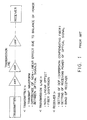
- Fig. 2 shows in the prior art the relation between pre-emphasis and an OSNR after transmission.
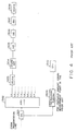
- Fig. 3 shows the configuration of a transmitter of the prior art.
- Fig. 4 shows the configuration of a receiver of the prior art.
- the transmitter has, for each wavelength, a laser diode driver (LD DRIVER) 1201, a laser diode (LD) 1202, an attenuator (ATT) 1203, a coupler (CPL) 1204, a post amplifier (POST AMP) 1205, and a photodiode (PD) 1208.
- the laser diode driver 1201 drives the laser diode 1202, while adjusting the output power and wavelength corresponding to each optical signal.
- the optical signal outputted from the laser diode 1202 is inputted to the post amplifier 1205 via the attenuator 1203 and the coupler 1204, and the optical signal is amplified in the post amplifier 1205.
- the optical signals, each of which is outputted from the post amplifier 1205, are multiplexed by an arrayed waveguide grating (AWG) 1206, and the multiplexed optical signal is outputted to a transmission line via a coupler 1207.
- AWG arrayed waveguide grating
- the coupler 1204 branches part of each optical signal to the photodiode 1208, resulting in part of the optical signal being detected by the photodiode 1208.
- the detection results are inputted to a CPU 1210.
- part of the transmitted optical signal which is outputted from the AWG 1206 to a transmission line, is branched and inputted to an optical spectrum analyzer 1209 by the coupler 1207.
- the optical spectrum analyzer 1209 monitors the peak power and wavelength of the transmitted optical signal, and notifies the CPU 1210 of the results.
- the CPU 1210 controls the laser diode driver 1201 and attenuator 1203 based on the output from the photodiode 1207 and optical spectrum analyzer 1209, for each optical signal.
- an optical signal received through a transmission line is inputted via a coupler 1301 to an AWG 1302, where the optical signal is demultiplexed into optical signals of various wavelengths.
- the receiver has, for each wavelength, a filter 1303 for separating an optical signal of a specific wavelength, an inline amplifier (INLINE AMP) 1304, a dispersion compensating fiber (DCF) 1305, an optical-electrical converter (O/E) 1306, a forward error corrector (FEC) 1307, and an electric-signal demultiplexer (DEMUX) 1308.
- a filter 1303 for separating an optical signal of a specific wavelength an inline amplifier (INLINE AMP) 1304, a dispersion compensating fiber (DCF) 1305, an optical-electrical converter (O/E) 1306, a forward error corrector (FEC) 1307, and an electric-signal demultiplexer (DEMUX) 1308.
- ILINE AMP inline amplifier
- DCF dispersion compensating fiber
- OFEC optical-electrical converter
- FEC forward error corrector
- DEMUX electric-signal demultiplexer
- the coupler 1301 branches part of a received optical signal into an optical spectrum analyzer 1309.
- the optical spectrum analyzer 1309 measures the OSNR for each optical signal received, and notifies a CPU 1310 of the results.
- the CPU 1310 feeds back the OSNR differences between optical signals received, as a pre-emphasis value, to the transmitting end by using a prescribed communications line.
- the CPU 1210 receives the above-mentioned pre-emphasis value, and controls the laser diode driver 1201 for each optical signal, based on the pre-emphasis value.
- the prior art is aware of an OSNR so as to optimize transmission characteristics, and makes uniform only an OSNR used for all optical signals.
- the most important factor of the transmission characteristics in digital transmission is a transmission error rate. Therefore, it is important to make uniform a transmission error rate for all optical signals in the optimization of transmission characteristics.
- the transmission error rate is not necessarily made uniform for all optical signals.
- the prior art has a problem, as shown in Fig. 5A, in that even if the OSNR is made uniform for optical signals 1, 2 and 3, the transmission error rate does not become uniform because of the difference of Q-values of the optical signals.
- the CPU 1210 directly changes the output power of the laser diode 1202 by controlling the laser diode driver 1201, for each optical signal.
- this method has a problem in that the setting of pre-emphasis for each optical signal must be repeated, while maintaining the power balance of optical signals, because the peak power of the other optical signals simultaneously change, resulting in the set value of pre-emphasis for each optical signal deviating from a proper value.
- the present invention aims at achieving real optimization of transmission characteristics, by making uniform a transmission error rate for all optical signals at the receiving end, based on the adjustment of an OSNR at the transmitting end.
- the present invention supposes an apparatus or method for making uniform transmission characteristics in the wavelength division multiplexing optical communications system.
- the apparatus according to a first aspect of the present invention has the following configuration.
- the relation between changes in a signal-to-noise ratio and changes in a transmission error rate at the receiving end is calculated for each optical signal to be wavelength-division-multiplexed.
- the signal-to-noise ratio for each optical signal is changed so as to attain a uniform transmission error rate for all optical signals at the receiving end.
- the apparatus according to a second aspect of the present invention has the following configuration.
- the difference between a reference value, which is the value of a signal-to-noise ratio corresponding to the target lower limit of a transmission error rate at the receiving end, and the value of a current signal-to-noise ratio is calculated as a margin.
- a signal-to-noise ratio is controlled so that the margin of the signal-to-noise ratio becomes equal to a prescribed value which is obtained from the margins calculated for the optical signals.
- the apparatus according to a third aspect of the present invention has the following configuration.
- the initial value of a signal-to-noise ratio is stored for each optical signal to be wavelength-division-multiplexed.
- an amplified spontaneous emission noise is superposed on the optical signal so as to gradually reduce the signal-to-noise ratio until a transmission error rate at the receiving end decreases to a target lower limit.
- the value of the corresponding signal-to-noise ratio is stored as a target lower limit, for each optical signal.
- the difference between the stored initial value and the stored target lower limit is calculated as a margin.
- the difference between a prescribed value which is obtained from the margins calculated for the optical signals, and the stored initial value is calculated as the pre-emphasis amount of the signal-to-noise ratio corresponding to the optical signal.
- the signal-to-noise ratio is controlled by superposing an amplified spontaneous emission noise corresponding to the pre-emphasis amount on the optical signal.
- the above-mentioned superposition of the amplified spontaneous emission noise on the optical signal is conducted at the transmitting end.
- the prescribed value which is obtained from the margins for optical signals, can be the average of the margins for the optical signals.
- either a Q-value or a bit error rate can be used as a transmission error rate.
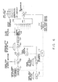
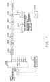
- Figs. 6 and 7 show the configuration of a transmitter and a receiver, respectively, according to a preferred embodiment of the present invention.
- Fig. 6 shows a laser diode driver 101, a laser diode 102, a coupler 103, a post amplifier 107, an AWG 109, a photodiode 110, a coupler 111, and an optical spectrum analyzer 112, which have the same functions as the matching components of the prior art, 1201, 1202, 1204, 1205, 1206, 1208, 1207, and 1209, respectively, as shown in Fig. 3.
- Fig. 7 shows a coupler 201, an AWG 202, a filter 203, an inline amplifier 204, a dispersion compensating fiber 205, an optical-electrical converter 207, a forward error corrector 208, an electric-signal demultiplexer 209, and an optical spectrum analyzer 213, which have the same functions as the matching components of the prior art, 1301-1309, respectively, as shown in Fig. 4.
- an ideal factor for transmission characteristics such as a Q-value and a BER
- This preferred embodiment includes the following features, which are the characteristics of the present invention: the relation between changes in an OSNR and changes in a Q-value or BER at the receiving end is calculated based on the relation as shown in Fig. 5B, so as to optimize transmission characteristics for each optical signal; and based on the calculation results, the OSNR for each optical signal is changed so as to make uniform the Q-value or BER for all optical signals at the receiving end.
- the difference between a reference value, which is the value of an OSNR at the transmitting end that corresponds to the target lower limit of a Q-value or BER at the receiving end, and the value of a current OSNR at the transmitting end is calculated as a margin for each optical signal. Then, the average of the margins for all optical signals are calculated, and pre-emphasis for the OSNR at the transmitting end is set for each optical signal so that the margin of the OSNR for each optical signal equals the average value. Note that in this process for controlling the OSNR for each optical signal, the amount of change in a Q-value or BER at the receiving end, per unit amount of change in an OSNR at the transmitting end, is assumed to be approximately uniform.
- part of each optical signal received which is separated by the coupler 206 as shown in Fig. 7, is inputted to a Q monitor (Q MON) 210, and is measured there.
- Q MON Q monitor
- the output from the forward error corrector 208 is inputted to a BER measuring unit 211, and is measured there.
- the multiplexed optical signal is amplified by the post amplifier 107, and then inputted to the AWG 109 via a narrow-band filter 108. Therefore, pre-emphasis can be set for all optical signals simultaneously, without losing the balance of power between the optical signals.
- the power and wavelength of the output from the laser diode 102 is monitored by the photodiode 110. Based on the monitoring results, a CPU 113 corrects the set value of the above-mentioned output power and wavelength, by performing a feedback to the laser diode driver 101.
- the output power of the amplified spontaneous emission noise outputted from the ASE output unit 104 is maintained so it is constant by an APC (automatic power control), and the wavelength characteristics of the amplified spontaneous emission noise are flat.
- the CPU 113 calculates and stores the initial value of an OSNR, E a1 , which is the ratio of the output power from the laser diode 102 that is detected by the photodiode 110 to the output power of an amplified spontaneous emission noise that is determined by the APC in the ASE output unit 104. In addition, the CPU 113 calculates the amount of change in an OSNR, as the amount of adjustment to be conducted by the attenuator 105.
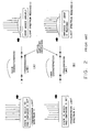
- Fig. 8 is a flowchart showing operations for achieving the above-mentioned function according to the preferred embodiment of the present invention
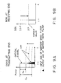
- Figs. 9A/B-11 are explanatory diagrams thereof. Note that the case in which a Q-value is monitored at the receiving end is assumed in the following explanations.
- the CPU 212 orders the transmitter to reduce an OSNR, by using a prescribed communications channel (step 301).
- the CPU 113 of the transmitter reduces the OSNR for each optical signal by directing the attenuator 105 to increase the amount of attenuation (step 302).
- the CPU 212 of the receiver determines, for each optical signal, whether the Q-value measured via the Q monitor 210 has decreased to the target lower limit (see Fig. 9B)(step 303).
- step 303 the CPU 212 of the receiver repeats the operations in steps 301 and 302 for each optical signal.
- the OSNR is reduced for each optical signal by gradually increasing an amplified spontaneous emission noise (ASE) to be superposed on the optical signal at the transmitting end, as shown in Fig. 9A, until the BER or Q-value at the receiving end decreases to the target lower limit, as shown in Fig. 9B.
- ASE amplified spontaneous emission noise
- step 303 the CPU 212 of the receiver orders the transmitter, by using the prescribed communications channel, to stop changing the OSNR, and restores the value of the OSNR to its initial value for each optical signal (step 304).
- the CPU 113 of the transmitter executes a series of processes as follows (step 305).
- E 1
- E AVG (E 1 + E 2 + --- + E n ) (n : the number of optical signals)
- the CPU 113 calculates a pre-emphasis value ⁇ E 1 ⁇ ⁇ E n , as given by the following equations, which is the difference between the average E AVG , as calculated according to Equation 2, and the margin of the OSNR for each optical signal, as calculated according to Equation 1 (see Fig. 10):
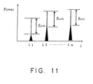
- the CPU 113 controls the OSNR for each optical signal so that the OSNR equals the average E AVG , by setting, for each optical signal, an amount of attenuation to be performed by the attenuator 105 that corresponds to the pre-emphasis amount ⁇ E 1 ⁇ ⁇ E n as calculated according to Equation 3 (see Fig. 11).
- the CPU 113 executes feedback control by monitoring the output from the optical spectrum analyzer 112 (Fig. 6) so that the OSNR for each optical signal is exactly equal to E AVG (step 306).
- pre-emphasis can be set according to customer demand, thereby allowing various operation forms, in which the setting of pre-emphasis is conducted, for example, regularly once a year, after repairs in the case of a problem with the system, and so on.
- Fig. 12 shows the configuration of a receiver according to another preferred embodiment of the present invention.
- the OSNR for each optical signal is measured by the optical spectrum analyzer 213, to which the output from the coupler 201 is inputted, and the peak power of each optical signal is measured by a photodiode 702, to which the output from the coupler 701 is inputted.
- the CPU 212 determines the amount of attenuation required by the attenuator 105 (a pre-emphasis value), and adjusts the OSNR for each optical signal.
- the Q monitor 210 After converting an optical signal into an electric signal, the Q monitor 210 measures the distribution of a noise by changing the distinguished value of a signal at each of the mark side and the space side on a eye-pattern, and measures an error rate at each of the mark side and the space side. Then the Q monitor 210 approximates each of two error rate curves, obtained as a result of the measurement, to a line, and calculates a Q-value by obtaining the intersection point of the two lines representing characteristics.
- Fig. 13 The relation between the eye-pattern and noise distribution of a signal can be shown by a model as shown in Fig. 13, wherein: P 1 (X) and P 0 (X) is a noise probability distribution function at the mark side and space side, respectively; ⁇ 1 and ⁇ 0 are the mean values of each probability distribution, and represent a signal level; and ⁇ 1 and ⁇ 0 are the variances of each probability distribution, and represent the RMS value of a noise.
- ( ⁇ 0 + ⁇ 1 ) Q dB 20LOG 10 ⁇
- ⁇ 0 , ⁇ 1 , ⁇ 0 , and ⁇ 1 are obtained, after a BER is obtained at two points on each of the mark side and the space side by changing a discrimination level as shown in Fig. 14. From these obtained values, ⁇ 0 , ⁇ 1 , ⁇ 0 , and ⁇ 1 can be calculated as shown by the following equation;
- Equation 4 a Q-value can be calculated.
Landscapes
- Engineering & Computer Science (AREA)
- Computer Networks & Wireless Communication (AREA)
- Signal Processing (AREA)
- Physics & Mathematics (AREA)
- Spectroscopy & Molecular Physics (AREA)
- Electromagnetism (AREA)
- Optical Communication System (AREA)
- Cable Transmission Systems, Equalization Of Radio And Reduction Of Echo (AREA)
- Noise Elimination (AREA)
- Reduction Or Emphasis Of Bandwidth Of Signals (AREA)
Applications Claiming Priority (2)
| Application Number | Priority Date | Filing Date | Title |
|---|---|---|---|
| JP36057298 | 1998-12-18 | ||
| JP36057298A JP3574578B2 (ja) | 1998-12-18 | 1998-12-18 | 波長分割多重光通信システムにおける伝送特性均一化装置及び方法 |
Publications (2)
| Publication Number | Publication Date |
|---|---|
| EP1011221A2 true EP1011221A2 (fr) | 2000-06-21 |
| EP1011221A3 EP1011221A3 (fr) | 2004-10-20 |
Family
ID=18469989
Family Applications (1)
| Application Number | Title | Priority Date | Filing Date |
|---|---|---|---|
| EP99114176A Withdrawn EP1011221A3 (fr) | 1998-12-18 | 1999-07-22 | Dispositif et procédé pour rendre les caractéristiques de transmission uniforme dans une système de communication optique à multiplexage de longueurs d'ondes |
Country Status (3)
| Country | Link |
|---|---|
| US (1) | US6445471B1 (fr) |
| EP (1) | EP1011221A3 (fr) |
| JP (1) | JP3574578B2 (fr) |
Cited By (4)
| Publication number | Priority date | Publication date | Assignee | Title |
|---|---|---|---|---|
| US7242865B2 (en) | 2001-12-03 | 2007-07-10 | Fujitsu Limited | Optical communication system |
| US7693423B2 (en) | 2002-06-11 | 2010-04-06 | Ericsson Ab | Maximising power in optical communication networks |
| EP3236597A1 (fr) * | 2016-04-19 | 2017-10-25 | Fujitsu Limited | Appareil de commande de réseau et procédé de calcul de marge de qualité de transmission |
| WO2020042252A1 (fr) * | 2018-08-31 | 2020-03-05 | 武汉联特科技有限公司 | Ensemble de transmission optique, et module optique |
Families Citing this family (30)
| Publication number | Priority date | Publication date | Assignee | Title |
|---|---|---|---|---|
| US6580531B1 (en) * | 1999-12-30 | 2003-06-17 | Sycamore Networks, Inc. | Method and apparatus for in circuit biasing and testing of a modulated laser and optical receiver in a wavelength division multiplexing optical transceiver board |
| JP2001251245A (ja) | 2000-03-03 | 2001-09-14 | Fujitsu Ltd | 波長分割多重光通信システムにおける伝送特性均一化装置、及び伝送特性均一化方法 |
| JP4588282B2 (ja) * | 2000-08-31 | 2010-11-24 | 富士通株式会社 | 光通信システムの立ち上げ方法およびチャンネル増減設方法、ならびに、コンピュータ読み取り可能な記録媒体 |
| DE10047342A1 (de) * | 2000-09-25 | 2002-05-08 | Siemens Ag | Verfahren zum Ausgleich von Kanalqualitätsunterschieden in einem WDM-System |
| US6980737B1 (en) * | 2000-10-16 | 2005-12-27 | Nortel Networks Limited | Method and apparatus for rapidly measuring optical transmission characteristics in photonic networks |
| US7181146B1 (en) * | 2001-01-17 | 2007-02-20 | Optical Communication Products, Inc. | Self-adjusting data transmitter |
| US7110676B2 (en) * | 2001-02-13 | 2006-09-19 | Tellabs Operations, Inc. | Power pre-emphasis for WDM transmission systems |
| DE10111497B4 (de) * | 2001-03-09 | 2007-01-11 | Siemens Ag | Verfahren zur Ermittlung der Signalqualität bei optischen Übertragungssystemen |
| JP4686906B2 (ja) | 2001-06-04 | 2011-05-25 | 株式会社日立製作所 | 波長多重用光伝送装置 |
| JP4665344B2 (ja) | 2001-06-04 | 2011-04-06 | 株式会社日立製作所 | 波長間レベル偏差や光sn偏差を補償する光伝送装置 |
| US20030058494A1 (en) * | 2001-06-27 | 2003-03-27 | Roberts Kim B. | Control of parameters in a global optical controller |
| US6614586B2 (en) * | 2001-07-30 | 2003-09-02 | Dorsal Networks, Inc. | Methods and systems for high performance, wide bandwidth optical communication systems using Raman amplification |
| JP3863058B2 (ja) * | 2001-09-13 | 2006-12-27 | 三菱電機株式会社 | 光受信装置 |
| WO2003042722A2 (fr) * | 2001-11-13 | 2003-05-22 | University Of Maryland Baltimore County | Systeme et procede de mesure de gigue temporelle tout optique |
| FR2832274B1 (fr) * | 2001-11-15 | 2006-08-25 | Alcatel Optronics | Procede de controle dynamique d'un module optique |
| US7239807B2 (en) * | 2002-02-07 | 2007-07-03 | Nortel Networks Limited | Variable clamp equalization method and apparatus |
| JP3934513B2 (ja) * | 2002-08-29 | 2007-06-20 | 富士通株式会社 | 非線形劣化を考慮したプリエンファシス制御方法 |
| JP4654560B2 (ja) * | 2003-02-10 | 2011-03-23 | 日本電気株式会社 | 光出力制御装置、光出力制御方法および光出力制御プログラム |
| DE60304486T2 (de) * | 2003-12-04 | 2006-09-07 | Alcatel | Übertragungssteuerung und -Verfahren zum Kanalausgleich in einem Wellenlängen-Multiplex-System |
| JP4435741B2 (ja) * | 2006-01-18 | 2010-03-24 | 富士通株式会社 | 光伝送装置 |
| JP5003391B2 (ja) * | 2007-10-01 | 2012-08-15 | 富士通株式会社 | 光伝送システムおよび光伝送方法 |
| JP5123876B2 (ja) * | 2009-03-03 | 2013-01-23 | 富士通テレコムネットワークス株式会社 | Wdm伝送システムとwdm伝送システムの光信号対雑音比算出方法及びwdm伝送装置 |
| JP4757938B2 (ja) * | 2009-09-24 | 2011-08-24 | 富士通株式会社 | プリエンファシス方法、光通信システム、および、制御装置 |
| JP5648436B2 (ja) * | 2010-11-12 | 2015-01-07 | 富士通株式会社 | プリエンファシス制御方法 |
| US9654223B2 (en) * | 2015-04-23 | 2017-05-16 | Fujitsu Limited | Superchannel power pre-emphasis based on transmission criteria |
| US10044440B2 (en) * | 2016-10-18 | 2018-08-07 | Fujitsu Limited | Noise margin monitor and control method |
| JP6819243B2 (ja) * | 2016-11-24 | 2021-01-27 | 富士通株式会社 | 光伝送特性測定装置及び方法 |
| US10200770B2 (en) * | 2017-04-07 | 2019-02-05 | Ciena Corporation | Management of flexible grid and supercarriers in optical networks using a data model |
| US10574391B2 (en) * | 2017-08-03 | 2020-02-25 | Facebook, Inc. | Adaptable forward error correction |
| US11536916B1 (en) * | 2021-05-10 | 2022-12-27 | Amazon Technologies, Inc. | Pathloss optimization for optical systems |
Family Cites Families (5)
| Publication number | Priority date | Publication date | Assignee | Title |
|---|---|---|---|---|
| JP3373332B2 (ja) * | 1995-05-26 | 2003-02-04 | Kddi株式会社 | プリエンファシス方式光波長多重通信方法および装置 |
| JPH0946318A (ja) * | 1995-08-01 | 1997-02-14 | Fujitsu Ltd | 波長多重光伝送システム及び該伝送システムに用いる光送信装置 |
| JP3720112B2 (ja) * | 1996-03-18 | 2005-11-24 | 富士通株式会社 | 波長分割多重が適用されるシステム及び光パワー制御装置 |
| JP3992811B2 (ja) * | 1997-08-01 | 2007-10-17 | 富士通株式会社 | 光伝送システム及び送信端局 |
| US6069718A (en) * | 1997-09-19 | 2000-05-30 | Nortel Networks Corporation | Distortion penalty measurement procedure in optical systems using noise loading |
-
1998
- 1998-12-18 JP JP36057298A patent/JP3574578B2/ja not_active Expired - Fee Related
-
1999
- 1999-07-21 US US09/358,372 patent/US6445471B1/en not_active Expired - Fee Related
- 1999-07-22 EP EP99114176A patent/EP1011221A3/fr not_active Withdrawn
Non-Patent Citations (1)
| Title |
|---|
| None |
Cited By (7)
| Publication number | Priority date | Publication date | Assignee | Title |
|---|---|---|---|---|
| US7242865B2 (en) | 2001-12-03 | 2007-07-10 | Fujitsu Limited | Optical communication system |
| US7376348B2 (en) | 2001-12-03 | 2008-05-20 | Fujitsu Limited | Optical communication system |
| US7693423B2 (en) | 2002-06-11 | 2010-04-06 | Ericsson Ab | Maximising power in optical communication networks |
| EP3236597A1 (fr) * | 2016-04-19 | 2017-10-25 | Fujitsu Limited | Appareil de commande de réseau et procédé de calcul de marge de qualité de transmission |
| US10177843B2 (en) | 2016-04-19 | 2019-01-08 | Fujitsu Limited | Network control apparatus and transmission quality margin calculation method |
| WO2020042252A1 (fr) * | 2018-08-31 | 2020-03-05 | 武汉联特科技有限公司 | Ensemble de transmission optique, et module optique |
| US11320609B2 (en) | 2018-08-31 | 2022-05-03 | Linktel Technologies Co., Ltd | Light emitting assembly and optical module |
Also Published As
| Publication number | Publication date |
|---|---|
| JP3574578B2 (ja) | 2004-10-06 |
| US6445471B1 (en) | 2002-09-03 |
| JP2000183818A (ja) | 2000-06-30 |
| EP1011221A3 (fr) | 2004-10-20 |
Similar Documents
| Publication | Publication Date | Title |
|---|---|---|
| US6445471B1 (en) | Apparatus and method for making transmission characteristics uniform in a wavelength division multiplexing optical communications system | |
| US6219162B1 (en) | Methods for equalizing WDM systems | |
| US8275269B2 (en) | Distributed Raman amplifier and optical communication system | |
| US6934479B2 (en) | Wavelength division multiplexing optical communication system and wavelength division multiplexing optical communication method | |
| US7391974B2 (en) | Wavelength division multiplexing optical transmission equipment and method of amplifying optical wavelength division multiplexed signals | |
| US5923453A (en) | Apparatus for measuring optical transmission line property and optical wavelength multiplexing transmission apparatus | |
| US6847788B2 (en) | System and method for equalizing transmission characteristics in wavelength division multiplexing optical communication system | |
| US6233076B1 (en) | Optical communications system | |
| US8351797B2 (en) | Repeater and repeating method | |
| US6452716B1 (en) | Amplitude modulation of a pump laser signal in a distributed raman amplifier | |
| EP0959578B1 (fr) | Système de multiplexage en longueurs d'ondes et terminaison correspondante | |
| US10608775B2 (en) | Optical transmission apparatus, optical transmission method, and optical transmission system | |
| US8055129B2 (en) | Alien wavelength channel balancing and line amplifier optimization | |
| US6400475B1 (en) | Optical transmission system and optical communications device | |
| EP0924888A2 (fr) | Méthode et dispositif à égalisation de canaux dans des systèmes de multiplexage d' ondes | |
| US11558113B2 (en) | Automatic measurement of the noise performance of a transponder | |
| US6963681B2 (en) | Automatic raman gain control | |
| US7280768B2 (en) | Method and system for handling optical signals | |
| US20020027704A1 (en) | Method, apparatus, and system for optical amplification | |
| CN108966687A (zh) | 在真实网络条件下确定通道osnr和通道osnr裕度 | |
| US20220368448A1 (en) | Optical transmission device, optical transmission system, and optical transmitting power control method | |
| US7039272B2 (en) | Optical transmission equipment with dispersion compensation, and dispersion compensating method | |
| US7006278B2 (en) | Wavelength-division multiplexing optical transmission system and repeater station therein | |
| CN102714554A (zh) | 用于服务中拉曼增益测量及监控的方法和设备 | |
| JP7722098B2 (ja) | 光受信機、及び光トランシーバモジュール |
Legal Events
| Date | Code | Title | Description |
|---|---|---|---|
| PUAI | Public reference made under article 153(3) epc to a published international application that has entered the european phase |
Free format text: ORIGINAL CODE: 0009012 |
|
| AK | Designated contracting states |
Kind code of ref document: A2 Designated state(s): AT BE CH CY DE DK ES FI FR GB GR IE IT LI LU MC NL PT SE |
|
| AX | Request for extension of the european patent |
Free format text: AL;LT;LV;MK;RO;SI |
|
| PUAL | Search report despatched |
Free format text: ORIGINAL CODE: 0009013 |
|
| AK | Designated contracting states |
Kind code of ref document: A3 Designated state(s): AT BE CH CY DE DK ES FI FR GB GR IE IT LI LU MC NL PT SE |
|
| AX | Request for extension of the european patent |
Extension state: AL LT LV MK RO SI |
|
| 17P | Request for examination filed |
Effective date: 20041223 |
|
| 17Q | First examination report despatched |
Effective date: 20050201 |
|
| AKX | Designation fees paid |
Designated state(s): DE FR GB |
|
| R17C | First examination report despatched (corrected) |
Effective date: 20050201 |
|
| STAA | Information on the status of an ep patent application or granted ep patent |
Free format text: STATUS: THE APPLICATION IS DEEMED TO BE WITHDRAWN |
|
| 18D | Application deemed to be withdrawn |
Effective date: 20130416 |