EP1011298A1 - Substrat zur bildung von speziellen mustern, und verfahren zur herstellung des substrats - Google Patents
Substrat zur bildung von speziellen mustern, und verfahren zur herstellung des substrats Download PDFInfo
- Publication number
- EP1011298A1 EP1011298A1 EP99919593A EP99919593A EP1011298A1 EP 1011298 A1 EP1011298 A1 EP 1011298A1 EP 99919593 A EP99919593 A EP 99919593A EP 99919593 A EP99919593 A EP 99919593A EP 1011298 A1 EP1011298 A1 EP 1011298A1
- Authority
- EP
- European Patent Office
- Prior art keywords
- affinity
- fluid
- region
- base
- specific
- Prior art date
- Legal status (The legal status is an assumption and is not a legal conclusion. Google has not performed a legal analysis and makes no representation as to the accuracy of the status listed.)
- Granted
Links
Images



Classifications
-
- H—ELECTRICITY
- H05—ELECTRIC TECHNIQUES NOT OTHERWISE PROVIDED FOR
- H05K—PRINTED CIRCUITS; CASINGS OR CONSTRUCTIONAL DETAILS OF ELECTRIC APPARATUS; MANUFACTURE OF ASSEMBLAGES OF ELECTRICAL COMPONENTS
- H05K3/00—Apparatus or processes for manufacturing printed circuits
- H05K3/02—Apparatus or processes for manufacturing printed circuits in which the conductive material is applied to the surface of the insulating support and is thereafter removed from such areas of the surface which are not intended for current conducting or shielding
-
- B—PERFORMING OPERATIONS; TRANSPORTING
- B41—PRINTING; LINING MACHINES; TYPEWRITERS; STAMPS
- B41M—PRINTING, DUPLICATING, MARKING, OR COPYING PROCESSES; COLOUR PRINTING
- B41M3/00—Printing processes to produce particular kinds of printed work, e.g. patterns
- B41M3/006—Patterns of chemical products used for a specific purpose, e.g. pesticides, perfumes, adhesive patterns; use of microencapsulated material; Printing on smoking articles
-
- H—ELECTRICITY
- H05—ELECTRIC TECHNIQUES NOT OTHERWISE PROVIDED FOR
- H05K—PRINTED CIRCUITS; CASINGS OR CONSTRUCTIONAL DETAILS OF ELECTRIC APPARATUS; MANUFACTURE OF ASSEMBLAGES OF ELECTRICAL COMPONENTS
- H05K3/00—Apparatus or processes for manufacturing printed circuits
- H05K3/10—Apparatus or processes for manufacturing printed circuits in which conductive material is applied to the insulating support in such a manner as to form the desired conductive pattern
- H05K3/18—Apparatus or processes for manufacturing printed circuits in which conductive material is applied to the insulating support in such a manner as to form the desired conductive pattern using precipitation techniques to apply the conductive material
- H05K3/181—Apparatus or processes for manufacturing printed circuits in which conductive material is applied to the insulating support in such a manner as to form the desired conductive pattern using precipitation techniques to apply the conductive material by electroless plating
- H05K3/182—Apparatus or processes for manufacturing printed circuits in which conductive material is applied to the insulating support in such a manner as to form the desired conductive pattern using precipitation techniques to apply the conductive material by electroless plating characterised by the patterning method
- H05K3/185—Apparatus or processes for manufacturing printed circuits in which conductive material is applied to the insulating support in such a manner as to form the desired conductive pattern using precipitation techniques to apply the conductive material by electroless plating characterised by the patterning method by making a catalytic pattern by photo-imaging
-
- Y—GENERAL TAGGING OF NEW TECHNOLOGICAL DEVELOPMENTS; GENERAL TAGGING OF CROSS-SECTIONAL TECHNOLOGIES SPANNING OVER SEVERAL SECTIONS OF THE IPC; TECHNICAL SUBJECTS COVERED BY FORMER USPC CROSS-REFERENCE ART COLLECTIONS [XRACs] AND DIGESTS
- Y10—TECHNICAL SUBJECTS COVERED BY FORMER USPC
- Y10T—TECHNICAL SUBJECTS COVERED BY FORMER US CLASSIFICATION
- Y10T428/00—Stock material or miscellaneous articles
- Y10T428/24—Structurally defined web or sheet [e.g., overall dimension, etc.]
- Y10T428/24802—Discontinuous or differential coating, impregnation or bond [e.g., artwork, printing, retouched photograph, etc.]
-
- Y—GENERAL TAGGING OF NEW TECHNOLOGICAL DEVELOPMENTS; GENERAL TAGGING OF CROSS-SECTIONAL TECHNOLOGIES SPANNING OVER SEVERAL SECTIONS OF THE IPC; TECHNICAL SUBJECTS COVERED BY FORMER USPC CROSS-REFERENCE ART COLLECTIONS [XRACs] AND DIGESTS
- Y10—TECHNICAL SUBJECTS COVERED BY FORMER USPC
- Y10T—TECHNICAL SUBJECTS COVERED BY FORMER US CLASSIFICATION
- Y10T428/00—Stock material or miscellaneous articles
- Y10T428/31504—Composite [nonstructural laminate]
- Y10T428/31652—Of asbestos
- Y10T428/31663—As siloxane, silicone or silane
Definitions
- a certain amount of a fluid must be uniformly bonded over the entire pattern formation region in order to form a thin film in the shape of a pattern having a specific surface area.
- the above-mentioned universal substrates were not well suited to such applications.
- a thin film formation method that involved the formation of a bank had numerous drawbacks; namely, the trouble it took to form the bank, the excessive bumpiness of the substrate surface resulting from the bank, and the necessity to select a bank material that would work with both the substrate surface and the fluid.
- Still another invention that achieves the second object is a method for manufacturing a substrate for forming a patterned film by causing a specific fluid to adhere, comprising the step of:
- the fluid that serves as the material for the film is supplied to a cavity designed so that it can be filled with a fluid from an ink jet recording head. Voltage is then applied to a piezoelectric element designed such that a volumetric change can be effected in the cavity, and droplets of fluid are discharged from a nozzle so that the fluid will adhere evenly over the entire surface of the pattern formation region.
- Whether or not affinity is exhibited here is determined by the properties of the fluid with which the pattern is to be formed. For instance, if the fluid is one that includes polar molecules, such as water, then the surface region having polar groups will exhibit an affinity, while the surface region not having polar groups will not exhibit an affinity. Conversely, if the fluid is one that does not include polar molecules, such as many organic media, then the surface region having polar groups will not exhibit an affinity, while the surface region not having polar groups will exhibit an affinity. Which fluid to use is determined by what kind of material will be used to form the thin film.
- the pattern non-formation region 11 is the material of the base so that it will not exhibit an affinity to the fluid.
- the non-affinity regions 111 of the pattern formation region 10 are portions where the surface of the base is exposed, just as with the pattern non-formation region 11.
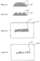
- the solvent component in the droplets will be removed when the droplets are dried, and the droplets will shrink in the position where they landed. Since there are no restrictions on the adhesion position, the droplets 12 that had initially linked together will split apart again and form islands 12b, as shown in Figures 5B and 6B. [A film] that splits up into the islands 12b will not work as a pattern.
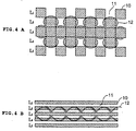
- the droplets 12 that land on the substrate spread out sufficiently in the affinity regions 110. They are rejected, however, by the non-affinity regions 111, and are drawn into the adjacent affinity regions 110 through surface tension. Therefore, after they are thus drawn by the action of their surface tension, the droplets 12 only adhere to the affinity regions 110, as shown in Figure 4A. Even though the direction in which the droplets are discharged from the head may vary somewhat, as long as the droplets 12 land in a specific width from lines L2 to L4, they will always adhere in the affinity regions 110 between lines L2 and L4. Since the affinity regions 110 are separated from one another, or only touch at points, the droplets 12 that are in a single affinity region 110 will not infiltrate adjacent affinity regions 110 unless they land directly thereon.
- the manufacture is such that a self-aggregating single-molecule film that exhibits no affinity remains in the pattern non-formation region 11 and in the non-affinity regions 111 in the pattern formation region 10. If the base 100 is formed from a material that exhibits no affinity to the fluid, then the manufacture is such that a self-aggregating single-molecule film that exhibits an affinity remains in the affinity regions 110 in the pattern formation region 10.
- a plasma treatment involves the surface modification of a substrate by performing a high-voltage glow discharge under a specific atmospheric pressure.
- an insulating substrate such as glass or plastic
- a crosslinked layer and a large number of unreacted groups are generated on the substrate surface.
- the unreacted groups are oxidized and form carbonyl groups or hydroxyl groups. Because these are polar groups, they have an affinity to a fluid containing polar molecules.
- most types of glass and plastic exhibit no affinity to a fluid containing polar molecules. Therefore, it is possible to produce affinity regions and non-affinity regions by selectively subjecting the pattern formation side of a substrate to a plasma treatment. This embodiment is based on this principle, and involves creating affinity regions and non-affinity regions by subjecting only part of the region to a plasma treatment by the use of a mask.
- the mask formation step is a step in which a mask 203 is applied over the base 100.
- a substrate such as glass on whose surface is formed a thin film of one of these plastics can also be used.
- the mask 203 is formed in a pattern such that the mask will cover only those regions of the base 100 that are to be made hydrophobic. For instance, when a fluid containing polar molecules is used, the mask is provided so that the affinity regions 110 in the pattern formation region 10 will be exposed and all other regions will be covered.
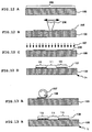
- Figure 12 illustrates the substrate manufacturing process in this Embodiment 7 in cross sections.
- the charge application step is a step in which a charge is generated on the base 100.
- a material that lends itself to charging is used for the base 100.
- the material is a polymer, polyethylene terephthalate can be used.
- a charge application means such as a corona charger used in a laser printer is used in order to apply a charge 205 to the base 100 surface.
- the substrate surface is uniformly charged by bringing the corona charger or other charge application means into proximity therewith.
- a DC high voltage of 6 to 8 kV is applied to a tungsten wire with a diameter of 50 to 100 ⁇ m, and corona discharge is performed 8 to 10 mm away from the base surface.
- the bonding step is a step in which electrostatic attraction is utilized to bond a powder material 107 [6] to the charged region that was not decharged.
- This powder material 107 is a material such as a toner for a laser printer, for instance, and a material that can be bonded by electrostatic force is used.
- the material used here becomes a surface that exhibits an affinity to a fluid containing polar molecules after fixing.
- This material can be steel, glass beads, iron powder, one of these that has been coated with a resin, a mixture of a magnetic material and a resin, or the like.
- the powder material 107 which has the opposite polarity from that of the charged region on the base 100, adheres by electrostatic force to the region where the charge 205 is present.
- the manufacture involves leaving a thin film of a powder material that exhibits no affinity in the pattern non-formation region 11 and the non-affinity regions 111 in the pattern formation region 10. If the base 100 is formed from a material that exhibits no affinity to the fluid, then the manufacture involves leaving a thin film of a powder material that exhibits an affinity in the affinity regions 110 in the pattern formation region 10.
- Embodiment 8 of the present invention relates to a manufacturing method in which a film is formed directly on a base by using a printing technique.
- Fixing step ( Figure 13B): Once the thin film material has been transferred to the base 100, a heat treatment or other known technique is applied in order to stabilize the thin film material 108. This step allows the manufacture of a substrate on which a thin film is formed only in the affinity regions 110 in the pattern formation region 10.
- the substrate of Embodiment 1 can be manufactured by utilizing a known printing method to bond a thin film material.
- the base 100 is formed from a material that exhibits an affinity to the fluid, then it is printed with a thin film exhibiting no affinity in the pattern non-formation region 11 and in the non-affinity regions 111 in the pattern formation region 10. If the base 100 is formed from a material that exhibits no affinity to the fluid, then it is printed with a thin film exhibiting an affinity in the affinity regions 110 in the pattern formation region 10.
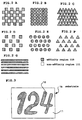
- the disposition of the affinity region and the pattern shapes in which the base is formed shown in Embodiment 1 are merely examples, and can be variously modified. Both a spotted pattern and a linear pattern can be variously modified in terms of the size, shape, and layout thereof. This is because these elements are determined according to the properties of the fluid.
- the method for manufacturing a substrate is not limited to those given in Embodiments 2 to 8 above, and various permutations thereof are possible, as long as [the substrate] is divided into a pattern formation region and a pattern non-formation region.
Landscapes
- Engineering & Computer Science (AREA)
- Chemical & Material Sciences (AREA)
- Chemical Kinetics & Catalysis (AREA)
- Microelectronics & Electronic Packaging (AREA)
- Manufacturing & Machinery (AREA)
- General Chemical & Material Sciences (AREA)
- Pest Control & Pesticides (AREA)
- Life Sciences & Earth Sciences (AREA)
- Application Of Or Painting With Fluid Materials (AREA)
- Manufacturing Of Printed Wiring (AREA)
- Other Surface Treatments For Metallic Materials (AREA)
- Structure Of Printed Boards (AREA)
- Particle Formation And Scattering Control In Inkjet Printers (AREA)
Applications Claiming Priority (3)
| Application Number | Priority Date | Filing Date | Title |
|---|---|---|---|
| JP13244698A JP3606047B2 (ja) | 1998-05-14 | 1998-05-14 | 基板の製造方法 |
| JP13244698 | 1998-05-14 | ||
| PCT/JP1999/002524 WO1999059386A1 (en) | 1998-05-14 | 1999-05-14 | Substrate for formation of special pattern, and method of manufacture of substrate |
Publications (3)
| Publication Number | Publication Date |
|---|---|
| EP1011298A1 true EP1011298A1 (de) | 2000-06-21 |
| EP1011298A4 EP1011298A4 (de) | 2003-08-27 |
| EP1011298B1 EP1011298B1 (de) | 2008-08-27 |
Family
ID=15081561
Family Applications (1)
| Application Number | Title | Priority Date | Filing Date |
|---|---|---|---|
| EP99919593A Expired - Lifetime EP1011298B1 (de) | 1998-05-14 | 1999-05-14 | Substrat zur bildung von speziellen mustern, und verfahren zur herstellung des substrats |
Country Status (7)
| Country | Link |
|---|---|
| US (2) | US6733868B1 (de) |
| EP (1) | EP1011298B1 (de) |
| JP (1) | JP3606047B2 (de) |
| KR (1) | KR100597015B1 (de) |
| CN (2) | CN1247054C (de) |
| DE (1) | DE69939420D1 (de) |
| WO (1) | WO1999059386A1 (de) |
Cited By (9)
| Publication number | Priority date | Publication date | Assignee | Title |
|---|---|---|---|---|
| WO2004106077A1 (en) * | 2003-05-29 | 2004-12-09 | 3M Innovative Properties Company | Method for modifying the surface of substrate |
| EP1357772A3 (de) * | 2002-04-22 | 2005-01-19 | Seiko Epson Corporation | Herstellungsverfahren von Leitern aus einer leitfähigen Schicht, Element mit geschichteter Struktur, elektrooptische Vorrichtung, und elektronisches Gerät |
| WO2005014184A1 (en) * | 2003-07-18 | 2005-02-17 | Eastman Kodak Company | Method of pattern coating |
| FR2872911A1 (fr) * | 2004-07-07 | 2006-01-13 | Commissariat Energie Atomique | Procede de localisation d'une espece chimique ou biologique sur un substrat, microsysteme d'analyse et biopuce |
| WO2006046009A1 (en) * | 2004-10-29 | 2006-05-04 | Eastman Kodak Company | Method of multilayered patterned coating |
| WO2007003720A1 (fr) * | 2005-07-01 | 2007-01-11 | Commissariat A L'energie Atomique | Revetement de surface hydrophobe et a faible hysteresis de mouillage, procede de depot d'un tel revetement, micro-composant et utilisation |
| WO2006072066A3 (en) * | 2004-12-30 | 2007-09-07 | Du Pont | Organic electronic devices and methods |
| WO2007133419A3 (en) * | 2006-05-02 | 2008-07-24 | Boston Scient Scimed Inc | Partially coated workpieces and method and system for making the same |
| EP2799154A1 (de) * | 2013-05-03 | 2014-11-05 | Nederlandse Organisatie voor toegepast -natuurwetenschappelijk onderzoek TNO | Schlitzblasbeschichtungsverfahren, Vorrichtung, und Substrat |
Families Citing this family (25)
| Publication number | Priority date | Publication date | Assignee | Title |
|---|---|---|---|---|
| JP3606047B2 (ja) * | 1998-05-14 | 2005-01-05 | セイコーエプソン株式会社 | 基板の製造方法 |
| JP2002340989A (ja) * | 2001-05-15 | 2002-11-27 | Semiconductor Energy Lab Co Ltd | 測定方法、検査方法及び検査装置 |
| US6973710B2 (en) * | 2001-08-03 | 2005-12-13 | Seiko Epson Corporation | Method and apparatus for making devices |
| JP4039035B2 (ja) | 2001-10-31 | 2008-01-30 | セイコーエプソン株式会社 | 線パターンの形成方法、線パターン、電気光学装置、電子機器、非接触型カード媒体 |
| US20030108725A1 (en) * | 2001-12-10 | 2003-06-12 | Matthew Hamilton | Visual images produced by surface patterning |
| GB0207350D0 (en) * | 2002-03-28 | 2002-05-08 | Univ Sheffield | Surface |
| JP2004066138A (ja) * | 2002-08-07 | 2004-03-04 | Fujimori Gijutsu Kenkyusho:Kk | 薄膜形成方法及びパターン形成方法並びにパターン形成装置 |
| GB0313569D0 (en) * | 2003-06-12 | 2003-07-16 | Plasso Technology Ltd | Method |
| KR100623227B1 (ko) * | 2004-05-27 | 2006-09-19 | 학교법인 영남학원 | 오프셋 인쇄방식을 이용한 적층형 전자소자 제조방법 |
| USD564721S1 (en) * | 2004-10-20 | 2008-03-18 | The Procter & Gamble Company | Cleaning article |
| DE102004058209A1 (de) * | 2004-12-02 | 2006-06-08 | Printed Systems Gmbh | Verfahren und Vorrichtung zur Erzeugung von Strukturen aus Funktionsmaterialien |
| JP4151652B2 (ja) * | 2005-01-11 | 2008-09-17 | セイコーエプソン株式会社 | 識別コード描画方法 |
| JP4929115B2 (ja) * | 2007-09-28 | 2012-05-09 | 本田技研工業株式会社 | 船外機用塗装金属製品及び同製造方法 |
| JP5206154B2 (ja) * | 2008-06-27 | 2013-06-12 | 富士通株式会社 | 配線基板の製造方法 |
| US8173552B2 (en) * | 2009-08-04 | 2012-05-08 | Intel Corporation | Method of fabricating an identification mark utilizing a liquid film assisted by a laser |
| JP5402511B2 (ja) * | 2009-10-19 | 2014-01-29 | セイコーエプソン株式会社 | 液晶装置及びその製造方法、並びに電子機器 |
| JP5797883B2 (ja) * | 2010-06-07 | 2015-10-21 | 住友電気工業株式会社 | プリント配線板用基板 |
| US8828484B2 (en) * | 2013-01-28 | 2014-09-09 | Taiwan Semiconductor Manufacturing Co., Ltd. | Self-alignment due to wettability difference of an interface |
| CN103213940B (zh) * | 2013-03-15 | 2016-04-06 | 北京工业大学 | 一种基于微纳米尺度使材料具有两种不同浸润性的方法 |
| USD765327S1 (en) * | 2013-06-27 | 2016-08-30 | The Procter & Gamble Company | Pad |
| US9305807B2 (en) * | 2014-02-27 | 2016-04-05 | Palo Alto Research Center Incorporated | Fabrication method for microelectronic components and microchip inks used in electrostatic assembly |
| WO2016194968A1 (ja) * | 2015-06-02 | 2016-12-08 | 株式会社村田製作所 | 金属層の形成方法 |
| DE102015224992A1 (de) * | 2015-12-11 | 2017-06-14 | Robert Bosch Gmbh | Verfahren zum mikrostrukturierten Aufbringen einer Flüssigkeit oder Paste auf eine Oberfläche |
| WO2019177120A1 (ja) * | 2018-03-16 | 2019-09-19 | Agc株式会社 | 膜付き基材 |
| JP2021181158A (ja) * | 2018-08-20 | 2021-11-25 | Agc株式会社 | 膜付き基材の製造方法 |
Family Cites Families (37)
| Publication number | Priority date | Publication date | Assignee | Title |
|---|---|---|---|---|
| DE519506C (de) * | 1929-03-31 | 1931-02-28 | Otto Marotz | Verfahren zum Auftragen farbiger Muster auf Leder u. dgl. |
| GB850934A (en) * | 1956-11-05 | 1960-10-12 | Keller Eberhard | Improvements in or relating to processes and apparatus for the production of coloured self-adhesive plates from aluminium foil |
| US3673961A (en) | 1960-04-27 | 1972-07-04 | Eastman Kodak Co | Xerothermographic process |
| NL139829B (nl) * | 1964-03-21 | 1973-09-17 | Philips Nv | Werkwijze voor de vervaardiging van lichtgevoelig materiaal, aldus vervaardigd lichtgevoelig materiaal en daarmee vervaardigd voorwerp. |
| US3554125A (en) | 1967-04-26 | 1971-01-12 | Xerox Corp | Method of making a lithographic master and method of printing therewith |
| JPS5143769A (en) | 1974-10-14 | 1976-04-14 | Asahi Chemical Ind | 11 beeta dd arabinofuranoshirushitoshinjudotaino seizoho |
| JPS574116B2 (de) * | 1975-02-07 | 1982-01-25 | ||
| JPS51106638A (en) * | 1975-03-17 | 1976-09-21 | Hitachi Ltd | Zetsuentaihyomenno fukatsuseikaho |
| JPS5240886A (en) | 1975-09-29 | 1977-03-30 | Toshiba Corp | Cutting method by ultra hard alloy of titanium nitride and cutting too ls |
| JPS51108638A (ja) * | 1976-02-23 | 1976-09-27 | Toyo Terumii Kk | Mudenkaibubunmetsukiho |
| JPS51115658A (en) | 1976-03-16 | 1976-10-12 | Matsushita Electric Industrial Co Ltd | Flux coating device |
| JPS58222592A (ja) * | 1982-03-15 | 1983-12-24 | イ−ストマン・コダツク・カンパニ− | 導電性パタ−ンの形成方法 |
| US4729310A (en) * | 1982-08-09 | 1988-03-08 | Milliken Research Corporation | Printing method |
| JPS5975205A (ja) | 1982-10-25 | 1984-04-27 | Seiko Epson Corp | カラ−フイルタの製造方法 |
| US5059513A (en) | 1983-11-01 | 1991-10-22 | Hoechst Celanese Corporation | Photochemical image process of positive photoresist element with maleimide copolymer |
| DE3535696C2 (de) * | 1985-10-05 | 1997-12-04 | Klaus Kalwar | Verfahren und Vorrichtung zur partiellen Beschichtung eines Kunststoffteiles |
| JPS6333895A (ja) * | 1986-07-29 | 1988-02-13 | キヤノン株式会社 | 電気回路の製造方法 |
| JPS63270474A (ja) * | 1986-12-10 | 1988-11-08 | Minoru Tsuda | 触媒性インク |
| US4879176A (en) * | 1987-03-16 | 1989-11-07 | Minnesota Mining And Manufacturing Company | Surface modification of semicrystalline polymers |
| JPS645095A (en) * | 1987-06-26 | 1989-01-10 | Tdk Corp | Formation of conductive pattern |
| US4833486A (en) * | 1987-07-08 | 1989-05-23 | Dataproducts Corporation | Ink jet image transfer lithographic |
| US4836105A (en) | 1987-12-10 | 1989-06-06 | International Business Machines Corporation | Direct negative and offset master production using thermal liftoff |
| IT1234203B (it) * | 1988-07-19 | 1992-05-06 | Elma S P A Santena To | Procedimento per la realizzazione di un riflettore per proiettore costituito da un tecnopolimero termoplastico e riflettore per proiettore realizzato tramite il suddetto procedimento |
| US5145758A (en) | 1988-07-29 | 1992-09-08 | Man Roland Druckmaschinen Ag | Method of producing a printing image carrier |
| US5272979A (en) | 1989-03-29 | 1993-12-28 | Presstek, Inc. | Plasma-jet imaging apparatus and method |
| US5254429A (en) | 1990-12-14 | 1993-10-19 | Anocoil | Photopolymerizable coating composition and lithographic printing plate produced therefrom |
| JPH05202483A (ja) * | 1991-04-25 | 1993-08-10 | Shipley Co Inc | 無電解金属化方法と組成物 |
| US5468597A (en) * | 1993-08-25 | 1995-11-21 | Shipley Company, L.L.C. | Selective metallization process |
| WO1995021030A1 (en) * | 1994-02-07 | 1995-08-10 | The Government Of The United States Of America, Represented By The Secretary Of The Navy | Efficient chemistry for selective modification and metallization of substrates |
| JPH07245467A (ja) * | 1994-03-07 | 1995-09-19 | Ibiden Co Ltd | プリント配線基板の製造方法 |
| EP0769331A1 (de) * | 1995-10-06 | 1997-04-23 | Ford Motor Company | Verfahren zur Identifizierung und zum Schutz einer aktivierten Kunststoffoberfläche |
| US5725788A (en) * | 1996-03-04 | 1998-03-10 | Motorola | Apparatus and method for patterning a surface |
| US5885753A (en) * | 1996-04-12 | 1999-03-23 | The Texas A&M University System | Polymeric self-assembled mono- and multilayers and their use in photolithography |
| AU6700998A (en) * | 1997-03-14 | 1998-09-29 | University Of Houston, The | Methods for making fluorinated surface modifying agents, methods of using same and products made using same |
| JPH1115000A (ja) * | 1997-06-26 | 1999-01-22 | Seiko Epson Corp | 液晶表示装置およびその製造方法 |
| KR100621851B1 (ko) * | 1998-01-28 | 2006-09-13 | 세이코 엡슨 가부시키가이샤 | 액체분출구조와, 잉크젯식 기록헤드 및 프린터 |
| JP3606047B2 (ja) * | 1998-05-14 | 2005-01-05 | セイコーエプソン株式会社 | 基板の製造方法 |
-
1998
- 1998-05-14 JP JP13244698A patent/JP3606047B2/ja not_active Expired - Fee Related
-
1999
- 1999-05-14 WO PCT/JP1999/002524 patent/WO1999059386A1/ja not_active Ceased
- 1999-05-14 DE DE69939420T patent/DE69939420D1/de not_active Expired - Lifetime
- 1999-05-14 KR KR1020007000370A patent/KR100597015B1/ko not_active Expired - Fee Related
- 1999-05-14 CN CNB99801138XA patent/CN1247054C/zh not_active Expired - Fee Related
- 1999-05-14 CN CNA2005100676068A patent/CN1697598A/zh active Pending
- 1999-05-14 EP EP99919593A patent/EP1011298B1/de not_active Expired - Lifetime
-
2000
- 2000-08-02 US US09/630,444 patent/US6733868B1/en not_active Expired - Lifetime
-
2004
- 2004-03-10 US US10/796,056 patent/US20040169004A1/en not_active Abandoned
Cited By (17)
| Publication number | Priority date | Publication date | Assignee | Title |
|---|---|---|---|---|
| EP1357772A3 (de) * | 2002-04-22 | 2005-01-19 | Seiko Epson Corporation | Herstellungsverfahren von Leitern aus einer leitfähigen Schicht, Element mit geschichteter Struktur, elektrooptische Vorrichtung, und elektronisches Gerät |
| WO2004106077A1 (en) * | 2003-05-29 | 2004-12-09 | 3M Innovative Properties Company | Method for modifying the surface of substrate |
| US6969166B2 (en) | 2003-05-29 | 2005-11-29 | 3M Innovative Properties Company | Method for modifying the surface of a substrate |
| WO2005014184A1 (en) * | 2003-07-18 | 2005-02-17 | Eastman Kodak Company | Method of pattern coating |
| FR2872911A1 (fr) * | 2004-07-07 | 2006-01-13 | Commissariat Energie Atomique | Procede de localisation d'une espece chimique ou biologique sur un substrat, microsysteme d'analyse et biopuce |
| WO2006005887A1 (fr) * | 2004-07-07 | 2006-01-19 | Commissariat A L'energie Atomique | Procede de localisation d'une espece chimique ou biologique sur un substrat, microsysteme d'analyse et biopuce |
| WO2006046009A1 (en) * | 2004-10-29 | 2006-05-04 | Eastman Kodak Company | Method of multilayered patterned coating |
| WO2006072066A3 (en) * | 2004-12-30 | 2007-09-07 | Du Pont | Organic electronic devices and methods |
| US8481104B2 (en) | 2004-12-30 | 2013-07-09 | E I Du Pont De Nemours And Company | Method of forming organic electronic devices |
| KR101290012B1 (ko) * | 2004-12-30 | 2013-07-30 | 이 아이 듀폰 디 네모아 앤드 캄파니 | 유기 전자 장치 및 방법 |
| WO2007003720A1 (fr) * | 2005-07-01 | 2007-01-11 | Commissariat A L'energie Atomique | Revetement de surface hydrophobe et a faible hysteresis de mouillage, procede de depot d'un tel revetement, micro-composant et utilisation |
| US7989056B2 (en) | 2005-07-01 | 2011-08-02 | Commissariat A L'energie Atomique | Hydrophobic surface coating with low wetting hysteresis, method for depositing same, microcomponent and use |
| WO2007133419A3 (en) * | 2006-05-02 | 2008-07-24 | Boston Scient Scimed Inc | Partially coated workpieces and method and system for making the same |
| EP2799154A1 (de) * | 2013-05-03 | 2014-11-05 | Nederlandse Organisatie voor toegepast -natuurwetenschappelijk onderzoek TNO | Schlitzblasbeschichtungsverfahren, Vorrichtung, und Substrat |
| WO2014178716A1 (en) * | 2013-05-03 | 2014-11-06 | Nederlandse Organisatie Voor Toegepast-Natuurwetenschappelijk Onderzoek Tno | Slot-die coating method, apparatus, and substrate |
| CN105358260A (zh) * | 2013-05-03 | 2016-02-24 | 荷兰应用自然科学研究组织Tno | 狭槽式模具涂布方法、设备和基底 |
| US9640760B2 (en) | 2013-05-03 | 2017-05-02 | Nederlandse Organisatie Voor Toegepast—Natuurwetenschappelijk Onderzoek Tno | Slot-die coating method, apparatus, and substrate |
Also Published As
| Publication number | Publication date |
|---|---|
| KR20010021806A (ko) | 2001-03-15 |
| CN1697598A (zh) | 2005-11-16 |
| WO1999059386A1 (en) | 1999-11-18 |
| EP1011298B1 (de) | 2008-08-27 |
| US20040169004A1 (en) | 2004-09-02 |
| KR100597015B1 (ko) | 2006-07-06 |
| CN1247054C (zh) | 2006-03-22 |
| EP1011298A4 (de) | 2003-08-27 |
| JP3606047B2 (ja) | 2005-01-05 |
| DE69939420D1 (de) | 2008-10-09 |
| CN1274516A (zh) | 2000-11-22 |
| JPH11330666A (ja) | 1999-11-30 |
| US6733868B1 (en) | 2004-05-11 |
Similar Documents
| Publication | Publication Date | Title |
|---|---|---|
| EP1011298A1 (de) | Substrat zur bildung von speziellen mustern, und verfahren zur herstellung des substrats | |
| JP3539179B2 (ja) | 基板、基板の製造方法、集積回路および集積回路の製造方法。 | |
| KR101105991B1 (ko) | 침착 및 패턴 공정 | |
| US20040035605A1 (en) | Methods and apparatus for manufacturing electronic and electromechanical elements and devices by thin-film deposition and imaging | |
| US20080233489A1 (en) | Method to form a pattern of functional material on a substrate using a stamp having a surface modifying material | |
| US20030211425A1 (en) | Photoimageable, aqueous acid soluble polyimide polymers | |
| EP2054233A1 (de) | Verfahren zur formung eines musters aus einem funktionsmaterial auf einem substrat | |
| KR940004732A (ko) | 패턴 형성 방법 및 패턴 형성에 사용하는 박막 형성 방법 | |
| WO2008118340A2 (en) | Method to form a pattern of functional material on a substrate including the treatment of a surface of a stamp | |
| WO2008124130A1 (en) | Method to form a pattern of functional material on a substrate using a mask material | |
| KR20090015634A (ko) | 표면특성을 이용한 금속패턴 형성방법 및 이에 따라 형성된금속패턴 | |
| JP3921917B2 (ja) | 微細構造体の製造方法 | |
| CN100574563C (zh) | 金属图形及其制造方法 | |
| JP2006021491A (ja) | 積層構造体、積層構造体を用いた光学素子、表示素子、演算素子及びこれらの製造方法 | |
| JP4100378B2 (ja) | パターン形成用基板およびその製造方法 | |
| JP4663206B2 (ja) | 導電性パターン形成体の製造方法 | |
| EP1356531A1 (de) | Verfahren zur herstellung einer bahn auf einem substrat | |
| JP4181481B2 (ja) | 基板 | |
| JP3956930B2 (ja) | 基板 | |
| JP4507893B2 (ja) | 配線基板 | |
| JP2009135123A (ja) | パターン形成装置 | |
| JPH09314891A (ja) | 電極体の製造方法 | |
| JPH09254427A (ja) | 電極の製造方法 | |
| WO2017018103A1 (ja) | 配線基板の製造方法、及び配線基板 |
Legal Events
| Date | Code | Title | Description |
|---|---|---|---|
| PUAI | Public reference made under article 153(3) epc to a published international application that has entered the european phase |
Free format text: ORIGINAL CODE: 0009012 |
|
| 17P | Request for examination filed |
Effective date: 20000114 |
|
| AK | Designated contracting states |
Kind code of ref document: A1 Designated state(s): DE FR GB NL |
|
| RIC1 | Information provided on ipc code assigned before grant |
Free format text: 7H 05K 1/02 A, 7H 05K 3/18 B, 7B 05D 1/32 B |
|
| A4 | Supplementary search report drawn up and despatched |
Effective date: 20030715 |
|
| RIC1 | Information provided on ipc code assigned before grant |
Ipc: 7B 05D 1/18 B Ipc: 7B 05D 3/06 B Ipc: 7B 05D 3/14 B Ipc: 7B 05D 1/32 B Ipc: 7H 05K 3/18 B Ipc: 7H 05K 1/02 A |
|
| 17Q | First examination report despatched |
Effective date: 20051230 |
|
| GRAP | Despatch of communication of intention to grant a patent |
Free format text: ORIGINAL CODE: EPIDOSNIGR1 |
|
| GRAS | Grant fee paid |
Free format text: ORIGINAL CODE: EPIDOSNIGR3 |
|
| GRAA | (expected) grant |
Free format text: ORIGINAL CODE: 0009210 |
|
| AK | Designated contracting states |
Kind code of ref document: B1 Designated state(s): DE FR GB NL |
|
| REG | Reference to a national code |
Ref country code: GB Ref legal event code: FG4D |
|
| REF | Corresponds to: |
Ref document number: 69939420 Country of ref document: DE Date of ref document: 20081009 Kind code of ref document: P |
|
| PG25 | Lapsed in a contracting state [announced via postgrant information from national office to epo] |
Ref country code: NL Free format text: LAPSE BECAUSE OF FAILURE TO SUBMIT A TRANSLATION OF THE DESCRIPTION OR TO PAY THE FEE WITHIN THE PRESCRIBED TIME-LIMIT Effective date: 20080827 |
|
| PLBE | No opposition filed within time limit |
Free format text: ORIGINAL CODE: 0009261 |
|
| STAA | Information on the status of an ep patent application or granted ep patent |
Free format text: STATUS: NO OPPOSITION FILED WITHIN TIME LIMIT |
|
| 26N | No opposition filed |
Effective date: 20090528 |
|
| REG | Reference to a national code |
Ref country code: FR Ref legal event code: PLFP Year of fee payment: 17 |
|
| PGFP | Annual fee paid to national office [announced via postgrant information from national office to epo] |
Ref country code: GB Payment date: 20150513 Year of fee payment: 17 Ref country code: DE Payment date: 20150506 Year of fee payment: 17 |
|
| PGFP | Annual fee paid to national office [announced via postgrant information from national office to epo] |
Ref country code: FR Payment date: 20150508 Year of fee payment: 17 |
|
| REG | Reference to a national code |
Ref country code: DE Ref legal event code: R119 Ref document number: 69939420 Country of ref document: DE |
|
| GBPC | Gb: european patent ceased through non-payment of renewal fee |
Effective date: 20160514 |
|
| REG | Reference to a national code |
Ref country code: FR Ref legal event code: ST Effective date: 20170131 |
|
| PG25 | Lapsed in a contracting state [announced via postgrant information from national office to epo] |
Ref country code: FR Free format text: LAPSE BECAUSE OF NON-PAYMENT OF DUE FEES Effective date: 20160531 Ref country code: DE Free format text: LAPSE BECAUSE OF NON-PAYMENT OF DUE FEES Effective date: 20161201 |
|
| PG25 | Lapsed in a contracting state [announced via postgrant information from national office to epo] |
Ref country code: GB Free format text: LAPSE BECAUSE OF NON-PAYMENT OF DUE FEES Effective date: 20160514 |