EP1012700B1 - Multiples machines a etats finis identiques paralleles qui partagent une logique combinatoire - Google Patents
Multiples machines a etats finis identiques paralleles qui partagent une logique combinatoire Download PDFInfo
- Publication number
- EP1012700B1 EP1012700B1 EP97931546A EP97931546A EP1012700B1 EP 1012700 B1 EP1012700 B1 EP 1012700B1 EP 97931546 A EP97931546 A EP 97931546A EP 97931546 A EP97931546 A EP 97931546A EP 1012700 B1 EP1012700 B1 EP 1012700B1
- Authority
- EP
- European Patent Office
- Prior art keywords
- output
- coupled
- input
- state
- integrated circuit
- Prior art date
- Legal status (The legal status is an assumption and is not a legal conclusion. Google has not performed a legal analysis and makes no representation as to the accuracy of the status listed.)
- Expired - Lifetime
Links
Images


Classifications
-
- G—PHYSICS
- G06—COMPUTING OR CALCULATING; COUNTING
- G06F—ELECTRIC DIGITAL DATA PROCESSING
- G06F5/00—Methods or arrangements for data conversion without changing the order or content of the data handled
- G06F5/06—Methods or arrangements for data conversion without changing the order or content of the data handled for changing the speed of data flow, i.e. speed regularising or timing, e.g. delay lines, FIFO buffers; over- or underrun control therefor
- G06F5/10—Methods or arrangements for data conversion without changing the order or content of the data handled for changing the speed of data flow, i.e. speed regularising or timing, e.g. delay lines, FIFO buffers; over- or underrun control therefor having a sequence of storage locations each being individually accessible for both enqueue and dequeue operations, e.g. using random access memory
-
- G—PHYSICS
- G06—COMPUTING OR CALCULATING; COUNTING
- G06F—ELECTRIC DIGITAL DATA PROCESSING
- G06F7/00—Methods or arrangements for processing data by operating upon the order or content of the data handled
-
- G—PHYSICS
- G06—COMPUTING OR CALCULATING; COUNTING
- G06F—ELECTRIC DIGITAL DATA PROCESSING
- G06F2207/00—Indexing scheme relating to methods or arrangements for processing data by operating upon the order or content of the data handled
- G06F2207/38—Indexing scheme relating to groups G06F7/38 - G06F7/575
- G06F2207/3804—Details
- G06F2207/386—Special constructional features
- G06F2207/3884—Pipelining
Definitions
- the present invention relates to the field of digital systems; and specifically to finite state machines.
- the present invention relates to integrated circuits which implement multiple finite state machines on the same die.
- Digital logic systems can be characterized as consisting of storage elements and logic elements. Examples of storage elements are flip/flops and read/write memory cells, while an examples of a logic elements are logic gates and adders. Storage elements are characterized as being able to record digital information for future use and to deliver the recorded information when it is needed. A storage element holding N-bits of information assumes one of 2 N specific states when it records a specific N-bit value. Logic elements produce digital outputs by processing and manipulating information either retrieved from storage elements or obtained from other sources. Digital systems are characterized by interconnections of combinatorial logic elements and storage elements.
- a registered storage element is an array of storage elements controlled by a common clock. Examples of registered storage elements include a flip-flop and a shift register.
- a finite state machine generally accepts digital signal inputs and produces digital signal outputs as a function of the inputs and the current values of the state variables.
- State variables are the digital information stored in specific storage elements which define the current state of a finite state machine.
- the next state of a finite state machine is determined as a function of the current state and the inputs.
- the production of the outputs and the determination of the next state is performed by combinatorial logic.
- a common practice in digital systems is triggering the overwriting the current state with the next state by a repetitive event Thus, state variable transitions occur at the rising edge of a clock, for example.
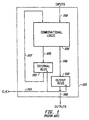
- FIG. 1 illustrates the classical model of a finite state machine 100.
- the finite state machine 100 there are two types of storage elements, internal registers 101 and output registers 102.
- the internal registers 101 store the current value of the state variables.
- the output registers 102 latch the output values of the finite state machine 100.
- Both the internal register 101 and the output register 103 have a dock (CLK) input 103, and therefore are updated once per dock cycle.
- the finite state machine is therefore a sequential circuit having feedback through the internal register 101.
- the combinatorial logic block 104 computes the next state 105 and the next output values 106 as a function of the current state and the current inputs.
- the current output values 109 are output by the output register 102.
- multiple independent identical parallel digital finite state machines can be integrated onto a single device.
- all elements of the finite state machine are replicated so that several complete independent circuits exist on the same die.
- the state machine 100 is replicated several times, as illustrated in Figure 2. This occurs, for example, when a single chip 200 serves as a transceiver for four independent communication channels.
- Four finite state machines 201-204 independently serve the four channels.
- all hardware components are replicated once for each independent state machine 201-204.
- the only connection between the independent state machines 201-204 are that they reside on the same integrated circuit die 200.
- Each finite state machine 201-204 is logically identical to the finite state machine 100 illustrated in Figure 1; therefore, each finite state machine 201-204 contains its own combinatorial logic 104, internal registers 101, and output registers 102.
- the pages of data are transferred to and from the automaton using the memory in a queue fashion (same output order as input order).
- a plurality of finite state machine perform their processes sharing the same black box, with the related data stored in a page circulating in the loop formed by the black box and the memory.
- the execution of the several Finite state machines are multiplexed in time sharing within the black box.
- An assembler and packer deal with the input and output, respectively, of the black box.
- An object of the present invention is to use the same combinatorial logic block to service multiple identical finite state machines. Another object of the present invention is to aggregate the state variable storage for the multiple finite state machines in a centralized memory unit.
- N separate finite state machines service N corresponding states.
- Other embodiments of the invention are specified in the respective appended dependent claims. It may be noted that each channel operating at a clock frequency F is serviced by the same combinatorial logic block which runs at an N*F clock frequency. Thus, if four finite state machines each run at 10 MHZ, the combinatorial logic is clocked at 40 MHZ and services each respective channel during every fourth dock cycle.
- the channel inputs are delivered to the combinatorial logic via an N-to-1 multiplexor.
- N separate output registers continuously provide output to the N separate channels. Each output register is loaded every Nth clock cycle.
- the sharing of the internal combinatorial logic according to the present invention is transparent to the devices connected to the integrated circuit, since the circuit according to the present invention implements N independent virtual machines which behave identically to N separate physical finite state machines.
- the state variables for each machine must be stored in a memory unit
- N separate state variable registers are loaded using the same load enable control signals as are used for the N output registers.
- the current state for the appropriate channel is selected by means of an N-to-1 multiplexor.
- an N-element shift register sequentially provides the appropriate channel's state variables to the shared combinatorial logic block. This embodiment has the simplest control, although it is not optimal in terms of power consumption, because all the state variables move every clock cycle rather than only every Nth clock cycle.
- a dual-ported Random Access Memory is used to efficiently aggregate the N channels' state variables. One port is dedicated to writing the next state while another port is dedicated to reading the current state.
- a read/write pointer is implemented as a counter which sequential count from 0 to N-1 such that the dual-ported RAM behaves identically to a shift register.
- the decoded counter value is also available to produce the control signals for the input multiplexor and the output register load enable signals.
- the shared combinatorial logic is pipelined into as many as N separate combinatorial logic sub-blocks.
- the latency from each channel's inputs to its outputs is increased by the number of pipeline flip-fops.
- the memory device for the state variables is reduced in size such that the total delay around the feedback loop equals the number of channels N.
- the memory device must behave like a twelve-deep shift register.
- the combinatorial logic is the exact same function relating next state and outputs to current state and inputs
- the combinatorial logic can be shared provided that the inputs of the combinatorial logic can be connected to the appropriate state variable outputs and state machine inputs while the outputs of the combinatorial logic can be connected to the appropriate state variable inputs and state machine outputs at the appropriate time.
- multiple independent parallel state machines share a common core of digital combinatorial logic.
- the independent storage elements can be consolidated in a memory array which can be addressed and accessed on a channel by channel basis.
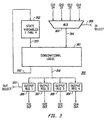
- Figure 3 illustrates an embodiment of the present invention.
- a single combinatorial unit 301 is shared amongst multiple channels. Channels one through four each have independent inputs (CH1IN-CH4IN) and outputs (CH1OUT-CH4OUT).
- the integrated circuit chip 300 according to the present invention implements four independent virtual state machines which behave identically to four independent physical state machines.
- the internal state variables for the four independent state machines are collected and centralized in a single memory unit 302.
- the channel input signals (CH1IN-CH4IN) are fimneled through a multiplexor 303.
- An input select signal IN SELECT 305 specifies which channel input signal (CH1IN-CH4IN) passes through the multiplexor 303 to the multiplexor output 304 and into the combinatorial logic 301 inputs.
- the current state for the appropriate channel 313 is output from the memory unit 302.
- Each of the output registers 306-309 corresponds to a separate channel.
- the combinatorial logic 301 computes the next output values 310 for a specific channel
- the corresponding one of the four output registers 306-309 is loaded as specified by the output select signal OUT SELECT 311.
- the next state variables 312 are computed by the combinatorial logic 301, they are stored in the memory unit 302, whose control will be described below in conjunction with its preferred and alternative embodiments.
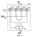
- Figure 4 illustrates one embodiment of the memory unit 302.
- the memory unit 302 is implemented as four separate state variable registers 401-404.
- a channel select signal CHANNEL SELECT 405 directs a multiplexor 406 to output the current state from the appropriate state variable register 401-404.
- the next state 312 is loaded into the selected register at the rising clock CLK 407 edge, for example.
- the channel select signal 405 enables loading for the selected channel.
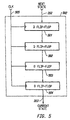
- Figure 5 illustrates another embodiment of the memory unit 302.
- the memory unit 302 is implemented as a four-element shift register consisting of D-type flip-flops 501-504 which shift state variable information forward each clock CLK 505 cycle.
- flip-flop 504 would hold state variable information for channel I while channel 2 state variable information is in flip-flop 503, channel 3 state variable information is in flip-flop 502, and channel 4 state variable information is in flip-flop 501.
- flip-flop 504 After the rising edge of the clock, flip-flop 504 would hold state variable information for channel 2, while channel 3 state variable information is in flip-flop 504, channel 4 state variable information is in flip-flop 502, and channel 1 state variable information is in flip-flop 501.
- the state variable information circulates around the shift register with each channel's state variable information occupying one of the flip-flops 501-504 at all times.
- FIG. 6 illustrates the preferred embodiment of the memory unit 302 according to the present invention.
- the next state 312 is input into a random access memory (RAM) array 607 write port.
- the clock CLK 603 drives a two-bit counter 604.
- the encoded two-bit output 605 of the counter 604 is decoded by the read address decoder 606 which produces the read word lines for the RAM array 607.
- the next state input 312 drives the write amplifiers (not shown) connected to the write port bit lines (not shown) of the RAM array 607.
- the read port bit lines of the RAM array 607 are interpreted by the sense amplifiers (not shown) which drive inputs 609 of the output flip-flop 602.
- the output flip-flop 602 changes its state at the rising edge of the clock 603.
- the read port reads one location ahead of the writing through me write port 312.
- a flip flop 610 delays the counter output 605 so that the decoded write address 613 is one location behind the decoded read address 614. Thus, during any given clock cycle, reading and writing are not being performed on the same memory location.
- the output select signal 311 is preferably an decoded set of load enable signals for the output registers 306-309.
- the control inputs 305 to the input multiplexor 303 are either encoded or decoded. If they are decoded, then they are logically equivalent to the output select signal 311.
- a decoder 615 produces the decoded control signals IN SELECT 305 and OUT SELECT 311 from the encoded counter output 612 output from the delay element 610.
- the decoder 615 is logically equivalent to the write address decoder 606 dedicated to the RAM array 607. Because the read access time from a RAM is typically greater than the write time, the flip-flop 602 is placed at the output. However, there is no requirement according to the present invention that flip-flop 602 be on the output. For example, the flip-flop 602 could alternatively buffer the input 312 of the write port of the RAM 607.
- Figure 7 illustrates a pipelined embodiment of the present invention.
- the combinatorial logic is separated into four separate logic networks 701-704.
- Three intermediate flip-flops 705-707 are used to separate four combinatorial logic modules 701-704.
- the state variable register 708 includes only one flip-flop 709 in this instance, because the total delay around the feedback loop must equal the number of channels. Because there are three flip-flops 705-707 in the combinatorial logic path and only four channels, only one flip-flop 709 is needed to store the state variables.
- the latency from inputs CH1IN-CH4IN to outputs CH1OUT-CH4OUT is four clock cycles rather than only one. Because each combinatorial logic module 701-704 operates on a different channel, the OUT SELECT control signal is no longer logically equivalent to the IN SELECT control signal, but rather is delayed by the number of intermediate flip-flops P. There is no requirement that the number of bits within each intermediate signal 710-712 is equal.
- the RAM ( Figure 6) or shift register ( Figure 5) embodiments of the memory unit are greatly preferred over the separate register/multiplexor embodiment ( Figure 4).
- This preference is based upon the fact that if the separate register/multiplexor embodiment is used, all sixteen (N) registers must be physically implemented rather than only twelve (N- # of pipeline stages P).
- the separate register/multiplexor embodiment involves simpler control in that the same control signal controls the input multiplexor and the state variable multiplexor, however it includes additional unnecessary registers.
- there are fewer state variable registers than channels therefore the address of the RAM in the embodiment of Figure 6 and the addressing of the input multiplexor 303 are different.
- the counter 604 addressing the RAM array repetitively counts from 0 to N-P-1.
- a separate input/output counter exists for the addressing of the input multiplexor and the output load enables.
- the input/output counter counts from 0 to N-1.
- the load enable signals are delayed by P clock cycles from the input multiplexor select signals.
- N minus P RAM memory locations it is sometimes preferable to implement all N locations within the memory array 607 so that the same memory location will always correspond to the same channel.
- the amount of delay introduced by the delay element 610 in Figure 6 is greater than one clock cycle; delay element 610 delays the counter 604 output 605 by P+1 clock cycles.
- the number of pipeline stages can vary from zero ( Figure 3) to one less than the number of channels ( Figure 7).
- the number of storage locations required in the preferred embodiments of the memory unit storing the state variables equals the number of channels minus the number of pipeline stages.
- the flip-flops 705-707 can alternatively be implemented as latches operating off alternate phases of the clock. Such that one half clock cycle delay is incurred at each latch.
- various alternative pipelining, memory addressing, and latching strategies can be employed to implement and control the shared combinational logic according to the present invention. For the sake of brevity, only the best modes of this state variable storage are described. Those skilled in the art will be enabled by this disclosure to construct various state variable first-in-first-out buffers using these and a variety of other designs.
- Products developed using the present invention include four 10/100 Megabit Ethernet transceiver channels integrated within a single integrated circuit device. Future products include the integration of twenty-four identical Media Access Control functions within a single integrated circuit.
Landscapes
- Engineering & Computer Science (AREA)
- Theoretical Computer Science (AREA)
- Physics & Mathematics (AREA)
- General Engineering & Computer Science (AREA)
- General Physics & Mathematics (AREA)
- Logic Circuits (AREA)
Claims (15)
- Dispositif à circuit intégré comportant N machines à états finis identiques distinctes pour desservir N canaux correspondants, le dispositif comprenant :un bloc de logique combinatoire (301) ayant une entrée d'état actuel (313), une entrée de canal (304) couplée de manière sélective auxdits N canaux, une sortie d'état suivant (312) et une sortie de canal (310) ;une unité de mémoire (302) ayant une entrée d'état suivant et une sortie d'état actuel (313) et comportant N emplacements de mémorisation de variables d'état correspondant aux N canaux, dans lequel l'entrée d'état suivant est couplée à la sortie d'état suivant du bloc de logique combinatoire, et dans lequel la sortie d'état actuel est couplée à l'entrée d'état actuel du bloc de logique combinatoire ; etN registres de sortie (306 à 309), chaque registre ayant une entrée et une sortie, dans lequel chacune des entrées est couplée à la sortie de canal du bloc de logique combinatoire, et dans lequel chacune des sorties est couplée à un canal correspondant parmi les N canaux.
- Dispositif à circuit intégré selon la revendication 1, dans lequel le dispositif comprend, de plus, un multiplexeur d'entrée (303) ayant N entrées et une sortie (304), dans lequel chacune des N entrées est couplée à un canal correspondant parmi les N canaux, et dans lequel la sortie est couplée à l'entrée de canal du bloc de logique combinatoire.
- Dispositif à circuit intégré selon la revendication 1 ou 2,
dans lequel l'unité de mémoire comprend :N registres de variable d'état (401, 402, 403, 404) ayant chacun une entrée et une sortie, dans lequel l'entrée est couplée à l'entrée d'état suivant ; etun multiplexeur de variables d'état (406) ayant N entrées et une sortie, dans lequel chacune des N entrées est couplée à une sortie correspondante parmi les N sorties de registre de variable d'état, dans lequel la sortie est couplée à la sortie d'état actuel. - Dispositif à circuit intégré selon la revendication 1 ou la revendication 2,
dans lequel l'unité de mémoire comprend :
un registre à décalage à N éléments (501, 502, 503, 504) ayant une entrée couplée à l'entrée d'état suivant et ayant une sortie couplée à la sortie d'état actuel. - Dispositif à circuit intégré selon la revendication 1 ou la revendication 2,
dans lequel l'unité de mémoire comprend :
une mémoire vive (607) ayant N emplacements, chaque emplacement correspondant à l'un des N canaux. - Dispositif à circuit intégré selon la revendication 5, comprenant, de plus :
un compteur (604) ayant une sortie de sélection de canal couplée à une entrée d'adresse de la mémoire vive. - Dispositif à circuit intégré selon la revendication 5,
dans lequel la mémoire vive a un port de lecture (614) et un port d'écriture (613), le port de lecture étant couplé à la sortie d'état actuel et le port d'écriture étant couplé à l'entrée d'état suivant. - Dispositif à circuit intégré selon la revendication 6,
dans lequel la sortie de sélection de canal du compteur est couplée à une entrée de commande du multiplexeur d'entrée et est couplée aux entrées d'autorisation de charge des N registres de sortie. - Dispositif à circuit intégré comportant N machines à états finis identiques distinctes pour desservir N canaux correspondants, le dispositif comprenant :un bloc de logique combinatoire en pipeline (701, 702, 703, 704) ayant une entrée d'état actuel, une entrée de canal, une sortie d'état suivant et une sortie de canal, dans lequel le bloc de logique combinatoire en pipeline comporte P éléments de registre de pipeline (705, 706, 707), de sorte que P soit inférieur à N ;un multiplexeur d'entrée ayant N entrées et une sortie, dans lequel chacune des N entrées est couplée à un canal correspondant parmi les N canaux, et dans lequel la sortie est couplée à l'entrée de canal du bloc de logique combinatoire ;une unité de mémoire ayant une entrée d'état suivant et une sortie d'état actuel et ayant au moins N - P emplacements de mémorisation de variables d'état (709), dans lequel l'entrée d'état suivant est couplée à la sortie d'état suivant du bloc de logique combinatoire, et dans lequel la sortie d'état actuel est couplée à l'entrée d'état actuel du bloc de logique combinatoire ; etN registres de sortie, chaque registre ayant une entrée et une sortie, dans lequel chacune des entrées est couplée à la sortie de canal du bloc de logique combinatoire, et dans lequel chacune des sorties est couplée à un canal correspondant parmi les N canaux.
- Dispositif à circuit intégré selon la revendication 9,
dans lequel l'unité de mémoire comprend :
un registre à décalage à N - P éléments ayant une entrée couplée à l'entrée d'état suivant et ayant une sortie couplée à la sortie d'état actuel. - Dispositif à circuit intégré selon la revendication 9,
dans lequel l'unité de mémoire comprend :
une mémoire vive (607). - Dispositif à circuit intégré selon la revendication 11, comprenant, de plus :
un compteur de canal (604) ayant une sortie de sélection de canal couplée à une entrée de sélection du multiplexeur d'entrée. - Dispositif à circuit intégré selon la revendication 12, dans lequel un signal d'autorisation de charge couplé aux N registres de sortie est la sortie de sélection de canal retardée de P cycles d'horloge.
- Dispositif à circuit intégré selon la revendication 12, dans lequel la mémoire vive comporte N - P emplacements, comprenant, de plus :
un compteur d'adresse de mémoire vive ayant une sortie d'adresse de mémoire vive couplée à la mémoire vive, dans lequel le compteur d'adresse de mémoire vive adopte de manière séquentielle N - P états, chaque état correspondant à un emplacement unique parmi les N - P emplacements. - Dispositif à circuit intégré selon la revendication 11,
dans lequel la mémoire vive a un port de lecture et un port d'écriture, le port de lecture étant couplé à la sortie d'état actuel et le port d'écriture étant couplé à l'entrée d'état suivant.
Applications Claiming Priority (3)
| Application Number | Priority Date | Filing Date | Title |
|---|---|---|---|
| US764212 | 1996-12-13 | ||
| US08/764,212 US5787273A (en) | 1996-12-13 | 1996-12-13 | Multiple parallel identical finite state machines which share combinatorial logic |
| PCT/US1997/011634 WO1998026348A1 (fr) | 1996-12-13 | 1997-07-01 | Multiples machines a etats finis identiques paralleles qui partagent une logique combinatoire |
Publications (2)
| Publication Number | Publication Date |
|---|---|
| EP1012700A1 EP1012700A1 (fr) | 2000-06-28 |
| EP1012700B1 true EP1012700B1 (fr) | 2001-09-26 |
Family
ID=25070013
Family Applications (1)
| Application Number | Title | Priority Date | Filing Date |
|---|---|---|---|
| EP97931546A Expired - Lifetime EP1012700B1 (fr) | 1996-12-13 | 1997-07-01 | Multiples machines a etats finis identiques paralleles qui partagent une logique combinatoire |
Country Status (3)
| Country | Link |
|---|---|
| US (1) | US5787273A (fr) |
| EP (1) | EP1012700B1 (fr) |
| WO (1) | WO1998026348A1 (fr) |
Families Citing this family (13)
| Publication number | Priority date | Publication date | Assignee | Title |
|---|---|---|---|---|
| US6799319B2 (en) | 2000-07-17 | 2004-09-28 | Sun Microsystems, Inc. | Method and apparatus for application packages and delegate packages to adopt and export standard execution state machine interfaces |
| US20030149629A1 (en) * | 2002-02-06 | 2003-08-07 | Claridge Bo. T. | Method of point of sale investment |
| JP2005524142A (ja) * | 2002-04-26 | 2005-08-11 | カリフォルニア・インスティテュート・オブ・テクノロジー | クロックレスにデータを復旧するシステム及び方法 |
| US7065602B2 (en) * | 2003-07-01 | 2006-06-20 | International Business Machines Corporation | Circuit and method for pipelined insertion |
| GB2403821B (en) * | 2003-07-07 | 2005-09-07 | Infineon Technologies Ag | Finite state machine circuit |
| GB2418520B (en) * | 2003-12-11 | 2006-06-07 | Lg Philips Lcd Co Ltd | Liquid crystal display device |
| KR100598738B1 (ko) | 2003-12-11 | 2006-07-10 | 엘지.필립스 엘시디 주식회사 | 액정표시장치와 그의 구동방법 |
| US7957172B2 (en) * | 2007-06-22 | 2011-06-07 | Broadcom Corporation | System for retaining state data of an integrated circuit |
| WO2011092548A1 (fr) * | 2010-01-26 | 2011-08-04 | Freescale Semiconductor, Inc. | Dispositif à circuit intégré et procédé d'utilisation de logique combinatoire dans circuit de traitement de données |
| US11449344B1 (en) * | 2020-04-21 | 2022-09-20 | Xilinx, Inc. | Regular expression processor and parallel processing architecture |
| US11983122B2 (en) | 2022-04-26 | 2024-05-14 | Xilinx, Inc. | High-throughput regular expression processing with path priorities using an integrated circuit |
| US12014072B2 (en) | 2022-04-26 | 2024-06-18 | Xilinx, Inc. | High-throughput regular expression processing using an integrated circuit |
| US11861171B2 (en) | 2022-04-26 | 2024-01-02 | Xilinx, Inc. | High-throughput regular expression processing with capture using an integrated circuit |
Family Cites Families (6)
| Publication number | Priority date | Publication date | Assignee | Title |
|---|---|---|---|---|
| US4740891A (en) * | 1985-05-06 | 1988-04-26 | Tektronix, Inc. | Asynchronous state machine |
| JPS6376610A (ja) * | 1986-09-19 | 1988-04-06 | Fujitsu Ltd | 遅延回路 |
| JPH05197741A (ja) * | 1991-06-06 | 1993-08-06 | Lsi Logic Corp | インターリーブド乗算器累算器 |
| US5394557A (en) * | 1992-12-30 | 1995-02-28 | Intel Corporation | State machine operating in multiple parallel phase and method thereof |
| US5680594A (en) * | 1995-05-24 | 1997-10-21 | Eastman Kodak Company | Asic bus interface having a master state machine and a plurality of synchronizing state machines for controlling subsystems operating at different clock frequencies |
| US5640398A (en) * | 1995-11-01 | 1997-06-17 | Pmc-Sierra, Inc. | State machine architecture for concurrent processing of multiplexed data streams |
-
1996
- 1996-12-13 US US08/764,212 patent/US5787273A/en not_active Expired - Lifetime
-
1997
- 1997-07-01 WO PCT/US1997/011634 patent/WO1998026348A1/fr not_active Ceased
- 1997-07-01 EP EP97931546A patent/EP1012700B1/fr not_active Expired - Lifetime
Also Published As
| Publication number | Publication date |
|---|---|
| US5787273A (en) | 1998-07-28 |
| WO1998026348A1 (fr) | 1998-06-18 |
| EP1012700A1 (fr) | 2000-06-28 |
Similar Documents
| Publication | Publication Date | Title |
|---|---|---|
| US5430687A (en) | Programmable logic device including a parallel input device for loading memory cells | |
| US5394031A (en) | Apparatus and method to improve programming speed of field programmable gate arrays | |
| EP0703663B1 (fr) | Module à retard numérique programmable | |
| US5463591A (en) | Dual port memory having a plurality of memory cell arrays for a high-speed operation | |
| US4380046A (en) | Massively parallel processor computer | |
| EP0701713B1 (fr) | Dispositif logique programmable par l'utilisateur avec interconnexions dymamiques a un tore logique dynamique | |
| US4553203A (en) | Easily schedulable horizontal computer | |
| JP3471088B2 (ja) | 改良されたプログラマブル論理セルアレイアーキテクチャ | |
| EP1012700B1 (fr) | Multiples machines a etats finis identiques paralleles qui partagent une logique combinatoire | |
| US4369500A (en) | High speed NXM bit digital, repeated addition type multiplying circuit | |
| US4326266A (en) | Monitoring system for a modular digital data processor | |
| US7355917B2 (en) | Two-dimensional data memory | |
| US3943347A (en) | Data processor reorder random access memory | |
| EP0520425B1 (fr) | Mémoire à semi-conducteur | |
| US4811201A (en) | Interconnect circuit | |
| US5805476A (en) | Very large scale integrated circuit for performing bit-serial matrix transposition operation | |
| US6104642A (en) | Method and apparatus for 1 of 4 register file design | |
| US5603046A (en) | Method for complex data movement in a multi-processor data processing system | |
| EP0256297A2 (fr) | Point de croisement pour élément binaire | |
| JPH0730407A (ja) | プログラム可能制御、デコード及び/又はデータ操作を有するレジスタファイル | |
| US5291457A (en) | Sequentially accessible non-volatile circuit for storing data | |
| US7190631B2 (en) | Multi-port memory | |
| US6642743B2 (en) | System for rapid configuration of a programmable logic device | |
| US6263482B1 (en) | Programmable logic device having macrocells with selectable product-term inversion | |
| US7203265B2 (en) | Synchronous counting circuit |
Legal Events
| Date | Code | Title | Description |
|---|---|---|---|
| PUAI | Public reference made under article 153(3) epc to a published international application that has entered the european phase |
Free format text: ORIGINAL CODE: 0009012 |
|
| 17P | Request for examination filed |
Effective date: 19990415 |
|
| AK | Designated contracting states |
Kind code of ref document: A1 Designated state(s): GB |
|
| GRAG | Despatch of communication of intention to grant |
Free format text: ORIGINAL CODE: EPIDOS AGRA |
|
| 17Q | First examination report despatched |
Effective date: 20010117 |
|
| GRAG | Despatch of communication of intention to grant |
Free format text: ORIGINAL CODE: EPIDOS AGRA |
|
| GRAG | Despatch of communication of intention to grant |
Free format text: ORIGINAL CODE: EPIDOS AGRA |
|
| GRAH | Despatch of communication of intention to grant a patent |
Free format text: ORIGINAL CODE: EPIDOS IGRA |
|
| GRAH | Despatch of communication of intention to grant a patent |
Free format text: ORIGINAL CODE: EPIDOS IGRA |
|
| GRAA | (expected) grant |
Free format text: ORIGINAL CODE: 0009210 |
|
| AK | Designated contracting states |
Kind code of ref document: B1 Designated state(s): GB |
|
| REG | Reference to a national code |
Ref country code: GB Ref legal event code: IF02 |
|
| PLBE | No opposition filed within time limit |
Free format text: ORIGINAL CODE: 0009261 |
|
| STAA | Information on the status of an ep patent application or granted ep patent |
Free format text: STATUS: NO OPPOSITION FILED WITHIN TIME LIMIT |
|
| 26N | No opposition filed | ||
| REG | Reference to a national code |
Ref country code: GB Ref legal event code: 732E Free format text: REGISTERED BETWEEN 20091126 AND 20091202 |
|
| PGFP | Annual fee paid to national office [announced via postgrant information from national office to epo] |
Ref country code: GB Payment date: 20100616 Year of fee payment: 14 |
|
| GBPC | Gb: european patent ceased through non-payment of renewal fee |
Effective date: 20110701 |
|
| PG25 | Lapsed in a contracting state [announced via postgrant information from national office to epo] |
Ref country code: GB Free format text: LAPSE BECAUSE OF NON-PAYMENT OF DUE FEES Effective date: 20110701 |