EP1014132A2 - Optisches Modul - Google Patents
Optisches Modul Download PDFInfo
- Publication number
- EP1014132A2 EP1014132A2 EP99125511A EP99125511A EP1014132A2 EP 1014132 A2 EP1014132 A2 EP 1014132A2 EP 99125511 A EP99125511 A EP 99125511A EP 99125511 A EP99125511 A EP 99125511A EP 1014132 A2 EP1014132 A2 EP 1014132A2
- Authority
- EP
- European Patent Office
- Prior art keywords
- lead frame
- electronic circuit
- wiring substrate
- encapsulating
- resin
- Prior art date
- Legal status (The legal status is an assumption and is not a legal conclusion. Google has not performed a legal analysis and makes no representation as to the accuracy of the status listed.)
- Withdrawn
Links
- 230000003287 optical effect Effects 0.000 title claims abstract description 120
- 239000000758 substrate Substances 0.000 claims abstract description 97
- 229920005989 resin Polymers 0.000 claims abstract description 96
- 239000011347 resin Substances 0.000 claims abstract description 96
- 238000012545 processing Methods 0.000 claims description 3
- 229910000679 solder Inorganic materials 0.000 claims description 2
- 238000005336 cracking Methods 0.000 abstract description 3
- 239000000463 material Substances 0.000 description 13
- 239000003822 epoxy resin Substances 0.000 description 8
- 238000000034 method Methods 0.000 description 8
- 229920000647 polyepoxide Polymers 0.000 description 8
- PNEYBMLMFCGWSK-UHFFFAOYSA-N aluminium oxide Inorganic materials [O-2].[O-2].[O-2].[Al+3].[Al+3] PNEYBMLMFCGWSK-UHFFFAOYSA-N 0.000 description 5
- 238000000465 moulding Methods 0.000 description 5
- 238000004891 communication Methods 0.000 description 4
- LNEPOXFFQSENCJ-UHFFFAOYSA-N haloperidol Chemical compound C1CC(O)(C=2C=CC(Cl)=CC=2)CCN1CCCC(=O)C1=CC=C(F)C=C1 LNEPOXFFQSENCJ-UHFFFAOYSA-N 0.000 description 4
- 239000002184 metal Substances 0.000 description 4
- 229910052751 metal Inorganic materials 0.000 description 4
- 239000000919 ceramic Substances 0.000 description 3
- 239000000945 filler Substances 0.000 description 3
- NJPPVKZQTLUDBO-UHFFFAOYSA-N novaluron Chemical compound C1=C(Cl)C(OC(F)(F)C(OC(F)(F)F)F)=CC=C1NC(=O)NC(=O)C1=C(F)C=CC=C1F NJPPVKZQTLUDBO-UHFFFAOYSA-N 0.000 description 3
- 239000013307 optical fiber Substances 0.000 description 3
- VYPSYNLAJGMNEJ-UHFFFAOYSA-N Silicium dioxide Chemical compound O=[Si]=O VYPSYNLAJGMNEJ-UHFFFAOYSA-N 0.000 description 2
- 238000005452 bending Methods 0.000 description 2
- 239000012141 concentrate Substances 0.000 description 2
- 239000000470 constituent Substances 0.000 description 2
- 229910052593 corundum Inorganic materials 0.000 description 2
- 230000009977 dual effect Effects 0.000 description 2
- 238000005538 encapsulation Methods 0.000 description 2
- 238000005530 etching Methods 0.000 description 2
- 238000012986 modification Methods 0.000 description 2
- 230000004048 modification Effects 0.000 description 2
- 238000003825 pressing Methods 0.000 description 2
- 238000004080 punching Methods 0.000 description 2
- 238000001721 transfer moulding Methods 0.000 description 2
- 229910001845 yogo sapphire Inorganic materials 0.000 description 2
- RYGMFSIKBFXOCR-UHFFFAOYSA-N Copper Chemical compound [Cu] RYGMFSIKBFXOCR-UHFFFAOYSA-N 0.000 description 1
- 239000004593 Epoxy Substances 0.000 description 1
- 229910000530 Gallium indium arsenide Inorganic materials 0.000 description 1
- ATJFFYVFTNAWJD-UHFFFAOYSA-N Tin Chemical compound [Sn] ATJFFYVFTNAWJD-UHFFFAOYSA-N 0.000 description 1
- 239000000853 adhesive Substances 0.000 description 1
- 230000001070 adhesive effect Effects 0.000 description 1
- 229910045601 alloy Inorganic materials 0.000 description 1
- 239000000956 alloy Substances 0.000 description 1
- 239000003990 capacitor Substances 0.000 description 1
- 229910010293 ceramic material Inorganic materials 0.000 description 1
- 239000011231 conductive filler Substances 0.000 description 1
- 229910052802 copper Inorganic materials 0.000 description 1
- 239000010949 copper Substances 0.000 description 1
- PMHQVHHXPFUNSP-UHFFFAOYSA-M copper(1+);methylsulfanylmethane;bromide Chemical compound Br[Cu].CSC PMHQVHHXPFUNSP-UHFFFAOYSA-M 0.000 description 1
- 230000003247 decreasing effect Effects 0.000 description 1
- 238000013461 design Methods 0.000 description 1
- 230000002542 deteriorative effect Effects 0.000 description 1
- 229910003460 diamond Inorganic materials 0.000 description 1
- 239000010432 diamond Substances 0.000 description 1
- 230000000694 effects Effects 0.000 description 1
- 238000005516 engineering process Methods 0.000 description 1
- 230000002349 favourable effect Effects 0.000 description 1
- 239000011521 glass Substances 0.000 description 1
- 238000010438 heat treatment Methods 0.000 description 1
- 238000004519 manufacturing process Methods 0.000 description 1
- 238000007639 printing Methods 0.000 description 1
- 239000004065 semiconductor Substances 0.000 description 1
- 239000000377 silicon dioxide Substances 0.000 description 1
- 229910052709 silver Inorganic materials 0.000 description 1
- 239000004332 silver Substances 0.000 description 1
- 229920001187 thermosetting polymer Polymers 0.000 description 1
Images


Classifications
-
- G—PHYSICS
- G02—OPTICS
- G02B—OPTICAL ELEMENTS, SYSTEMS OR APPARATUS
- G02B6/00—Light guides; Structural details of arrangements comprising light guides and other optical elements, e.g. couplings
- G02B6/24—Coupling light guides
- G02B6/42—Coupling light guides with opto-electronic elements
- G02B6/4201—Packages, e.g. shape, construction, internal or external details
- G02B6/4251—Sealed packages
- G02B6/4253—Sealed packages by embedding housing components in an adhesive or a polymer material
-
- G—PHYSICS
- G02—OPTICS
- G02B—OPTICAL ELEMENTS, SYSTEMS OR APPARATUS
- G02B6/00—Light guides; Structural details of arrangements comprising light guides and other optical elements, e.g. couplings
- G02B6/24—Coupling light guides
- G02B6/42—Coupling light guides with opto-electronic elements
- G02B6/4201—Packages, e.g. shape, construction, internal or external details
- G02B6/4274—Electrical aspects
-
- G—PHYSICS
- G02—OPTICS
- G02B—OPTICAL ELEMENTS, SYSTEMS OR APPARATUS
- G02B6/00—Light guides; Structural details of arrangements comprising light guides and other optical elements, e.g. couplings
- G02B6/24—Coupling light guides
- G02B6/42—Coupling light guides with opto-electronic elements
- G02B6/4201—Packages, e.g. shape, construction, internal or external details
- G02B6/4256—Details of housings
- G02B6/4262—Details of housings characterised by the shape of the housing
- G02B6/4265—Details of housings characterised by the shape of the housing of the Butterfly or dual inline package [DIP] type
Definitions
- the present invention relates to an optical module comprising an optical device which is a light-receiving device or light-emitting device.
- Optical modules such as receiving modules and transmitting modules are used in optical communication systems such as optical data links, optical LAN, and the like.
- a receiving module is equipped with a light-receiving device, for converting an optical signal transmitted through an optical fiber into an electric signal and outputting thus obtained electric signal; and
- a transmitting module is equipped with a light-emitting device, for converting an electric signal into an optical signal and sending out thus obtained optical signal to an optical fiber.
- Conventional examples of such optical modules are disclosed in Japanese Utility Model Application Laid-Open No. HEI 2-126107 and Japanese Patent Application Laid-Open No. HEI 2-278212.
- An optical module comprises an optical device which is a light-receiving device or light-emitting device, and an electronic circuit connected to the optical device.
- electronic components and wiring patterns constituting the electronic circuit are formed on a substrate or an island portion (substrate portion) of a lead frame functioning as a substrate, whereas the wiring pattern on the substrate and lead pins are connected to each other by wire bonding.
- the electronic circuit and substrate, and individual components such as a metal package including an optical device are integrally molded with an insulating molding resin, so as to construct the optical module.
- the lead frame is formed by such a method as etching a sheet material or punching it with a pressing machine, whereby the wiring pattern of the electronic circuit is formed as well. Since the lead frame is formed from a single sheet material as such, however, cross wiring by which two or more wires are crossed cannot be made, whereby the degree of freedom in the electronic circuit configuration would be limited. For this matter, cross wiring may be realized by carrying out wire bonding in a part where crossing is necessary. In this case, however, impedance mismatching may occur, thus deteriorating circuit characteristics of the electronic circuit.
- an object of the present invention to provide an optical module having a configuration which can increase the flexibility of its electronic circuit.
- the optical module in accordance with the present invention is an optical module comprising an optical device for converting one of an optical signal having a predetermined wavelength and an electric signal corresponding thereto into the other signal, an electronic circuit for processing the electric signal, and a lead frame having a lead pin connected to the electronic circuit; wherein a wiring substrate formed with at least a part of the electronic circuit is secured to one surface of the lead frame; wherein an electrode provided in the wiring substrate and a connecting portion provided in the lead frame are directly connected to each other, so that the electronic circuit on the wiring substrate and the lead frame are electrically connected to each other, the wiring substrate and the connecting portion of the lead frame being encapsulated with a resin so as to form an electronic circuit encapsulating portion; and wherein, in the electronic circuit encapsulating portion, a difference between a thickness of the encapsulating resin on the one surface of the lead frame from a surface of the wiring substrate opposite from the lead frame and a thickness of the encapsulating resin on the other surface of the lead frame is smaller
- the degree of freedom in the electronic circuit configuration can be enhanced such that cross wiring is formed within the substrate, for example.
- the wiring pitch can be made sufficiently small, so as to meet increase in the complexity of electronic circuits.
- the connecting portion is provided in the lead frame so as to face the electrode in the wiring substrate.
- the electrode and the connecting portion are secured and electrically connected to each other by use of an electrically conductive connecting member or the like.
- the encapsulated resin may break after the encapsulation.
- the encapsulating resin of the electronic circuit encapsulating portion is a transparent resin
- a transparent epoxy resin for example, has a thermal expansion coefficient on the order of 6.2 to 17.2 ⁇ 10 -5 /°C, which is at least 2 times larger than that of normal epoxy resins.
- a ceramic substrate such as alumina (Al 2 O 3 ), which is often used as a wiring substrate, has a thermal expansion coefficient of about 5.5 ⁇ 10 -6 /°C , for example, thus yielding a difference of 10 times or greater therebetween. Though the difference is slightly smaller as compared with the transparent epoxy resin, similar problems exist in the normal epoxy resins as well.
- the encapsulating resin on the wiring substrate will become thinner than the thickness of the encapsulating resin on the other side by the thickness of the wiring substrate.
- stresses generated in the respective resin portions would be out of balance, whereby distortions and cracks in the encapsulating resin may occur at the portions where excessive stresses concentrate.
- the difference between the thickness of the encapsulating resin on the upper side of the lead frame excluding the wiring substrate and the thickness of the encapsulating resin on the lower side of the lead frame is set so as to become smaller than the thickness of the wiring substrate by modifying the form of the encapsulating portion, arranging the position of the wiring substrate within the encapsulating resin, adding other members, and the like.
- concentration of excessive stresses are alleviated, so that distortions and cracks of the encapsulating resin can be prevented, whereby a resin molded package with a high reliability can be realized.
- it enables the resin molded package to become thinner.
- an optical module having a configuration in which, while the electronic circuit has a larger scale, the stability and reliability are maintained.
- the above-mentioned thickness condition concerning the encapsulating resin on both of the upper and lower sides of the lead frame may not necessarily be applied to the whole electronic circuit encapsulating portion. For example, if the above-mentioned thickness condition is applied to the resins just above the substrate and just beneath the substrate, then the encapsulating resin can be prevented from being distorted and cracking.
- the upward and downward directions in lead frames and wiring substrates will be defined. While a wiring substrate is mounted on one surface of a lead frame in each of the following optical modules, the directions toward this one surface and the other surface as seen from the lead frame are defined as upward and downward directions, respectively.
- the surface of the side mounted with the wiring substrate and the surface on the opposite side are defined as upper and lower faces, respectively.
- the surface mounted with electronic components on the opposite side from the lead frame and the surface on the lead frame side are defined as upper and lower faces, respectively.
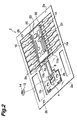
- Fig. 1 is a perspective view showing the exterior configuration of a first embodiment of the optical module in accordance with the present invention.
- an optical device is resin-encapsulated in an optical device encapsulating portion 16
- an electronic circuit is resin-encapsulated in an electronic circuit encapsulating portion 18, independently from each other.
- the optical device encapsulating portion 16 and the electronic circuit encapsulating portion 18 are connected to each other by means of inner lead pins 8.
- This optical module is of DIP (dual inline package) type, so that outer lead pins 10 project from both sides of the electronic circuit encapsulating portion 18.
- a metal lead frame 2 having the structure shown in Fig. 2 is used.
- the lead frame 2 is formed with an optical device mounting section 4 for mounting an optical device 14, 2 inner lead pins 8 for connecting the optical device mounting section 4 and the electronic circuit to each other, and 14 outer lead pins 10 in total disposed 7 by 7 on both sides of a wiring substrate which will be explained later.
- Respective parts of the inner lead pins 8 and outer lead pins 10 on the wiring substrate side are provided with connecting portions 8a and 10a.
- the lead frame 2 is integrally formed as a whole by etching a thin sheet made of a metal (e.g., copper) having a thickness of about 0.25 mm or punching it with a pressing machine, for example.
- Individual parts such as the above-mentioned optical device mounting section 4 are formed as being integrally supported by a frame portion 2a of the lead frame 2.
- the lead frame 2 is formed with a plurality of engagement holes 2b for positioning a resin molding die which will be explained later.
- the optical device 14 in the form of a semiconductor chip (bare chip) is secured onto the optical device mounting section 4.
- a parallel electrode type capacitor (Die Capacitance) or the like is employed as the sub-mount member 12
- a light-receiving device such as InGaAs-PIN type photodiode sensitive to an optical signal in the 1.3- ⁇ m wavelength band or the like is employed as the optical device 14.
- the sub-mount member 12 is a member for dissipating heat and is formed from diamond or an aluminum nitride material, whereas a light-emitting device such as a surface-emitting InGaAsP light-emitting diode adapted to emit an optical signal in the 1.3- ⁇ m wavelength band or a surface-emitting InGaAs laser diode is employed as the optical device 14.
- a light-emitting device such as a surface-emitting InGaAsP light-emitting diode adapted to emit an optical signal in the 1.3- ⁇ m wavelength band or a surface-emitting InGaAs laser diode is employed as the optical device 14.
- a wiring substrate 20 is mounted on the upper face side of the connecting portions 8a and 10a.
- electronic components such as an IC 22 are mounted, and a wiring pattern (schematically shown in Fig. 2) is formed, so as to constitute an electronic circuit for processing electric signals.
- electrodes 20a are disposed at their respective positions corresponding to the connecting portions 8a and 10a.
- the connecting portions 8a and 10a and the electrodes 20a are electrically connected to each other by means of an electrically conductive connecting material.
- a substrate-shaped auxiliary member 30 Secured to the lower face side of the connecting portions 8a and 10a is a substrate-shaped auxiliary member 30 which is made of a material identical to that of the wiring substrate 20 and has a form substantially identical thereto.
- a normal adhesive having no electric conductivity may be used therefor.
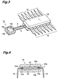
- a resin molding die having a predetermined form is positioned and attached to the lead frame 2 by means of the engagement holes 2b. Then, a resin transparent to an optical signal having a predetermined wavelength (e.g., 1.3 ⁇ m) is injected into this die, and the optical device 14 and the electronic circuit are resin-encapsulated separately from each other by a transfer-molding process (see Fig. 3).
- a resin transparent to an optical signal having a predetermined wavelength e.g., 1.3 ⁇ m
- the optical device encapsulating portion 16 for integrally encapsulating the optical device mounting section 4 and the sub-mount member 12 and optical device 14 mounted therewith, and the electronic circuit encapsulating portion 18 for integrally encapsulating the connecting portions 8a and 10a and the wiring substrate 20 and auxiliary member 30 mounted therewith are molded.
- the optical device encapsulating portion 16 for encapsulating the optical device 14 may be molded with a transparent resin
- the electronic circuit encapsulating portion 18 may be molded with a nontransparent resin.
- the optical device encapsulating portion 16 has a base 16a, having a substantially rectangular parallelepiped form, for encapsulating the optical device mounting section 4, the sub-mount member 12, and the optical device 14; a pedestal 16b integrally molded on the base 16a and shaped like a circular truncated cone; and an aspherical lens 16c integrally molded at the apex part of the pedestal 16b.
- the optical axis of the aspherical lens 16c and that of the optical main surface (light-receiving surface or light-emitting surface) of the optical device 14 coincide with each other.
- the pedestal 16b is formed as a circular truncated cone, concentric with the optical axis of the aspherical lens 16c and optical device 14, having a side face with a predetermined angle of inclination and a predetermined height so as to taper down toward the apex part thereof.
- the wiring pattern of the electronic circuit is not formed by the lead frame and wire bonding alone, but the wiring substrate 20 is mounted on the connecting portions 8a and 10a of the lead frame 2.
- a wiring pattern is formed on this wiring substrate 20, cross connection schematically indicated by numeral 24 in Fig. 2, for example, can easily be realized.
- Such cross wiring is free from the problem of impedance mismatch occurred in the cross wiring formed by bonding wire connection between wiring patterns provided by a lead frame, whereby favorable circuit characteristics can be obtained.
- the wiring pitch can be made smaller than that in the wiring pattern provided by the lead frame, the wiring can be made more efficiently, so as to meet increases in the complexity of electronic circuits.
- the electrodes 20a are disposed on the lower face side of the wiring substrate 20 at parts respectively facing the connecting portions 8a and 10a of the lead frame 2.
- the connecting portions 8a and 10a and the electrodes 20a are secured as shown in Fig. 4 by die bonding by way of an electrically conductive connecting material, so as to electrically connect the electronic circuit on the wiring substrate 20 and the lead frame 2 to each other.
- connecting portions 8a and 10a are connected to their corresponding inner lead pins 8 and outer lead pins 10, necessary connection can be realized thereby without wire bonding.
- an electrically conductive resin can be used as the above-mentioned electrically conductive connecting material.
- the electrically conductive resin include resins containing an electrically conductive filler made of Ag (silver) and the like. Alternatively, solder such as Sn (tin)/Pb (lead) alloy can be used.
- the supporting of the wiring substrate 20 by the lead frame 2 may be realized by the above-mentioned securing onto the connecting portions 8a and 10a alone, or by forming the lead frame 2 with a support portion for the wiring substrate 20.
- the coefficient of thermal expansion of the wiring substrate 20 and that of the encapsulating resin constituting the electronic circuit encapsulating portion 18 are greatly different from each other.
- the encapsulating resin of the electronic circuit encapsulating portion 18 is a transparent resin
- a thermal expansion coefficient of a transparent epoxy resin is in the order of 6.2 to 17.2 ⁇ 10 -5 /°C, which is at least 2 times that of normal epoxy resins.
- a ceramic substrate such as alumina (Al 2 O 3 ), which is often used as the wiring substrate 20, has a thermal expansion coefficient of about 5.5 ⁇ 10 -6 /°C, for example, thus yielding a difference of 10 times or greater therebetween. Though the difference is slightly smaller as compared with the transparent epoxy resin, similar problems exist in the normal epoxy resins as well.
- Resin encapsulation is carried out by a transfer-molding process using a thermosetting resin, in which the resin injected into a die is cured as being heated and held at a temperature of the molding for a predetermined time, so as to form the encapsulating portions. While the heating temperature at this time is set to about 140 to 160°C in the case of a transparent resin, for example, a large stress is generated in the encapsulating resin due to the above-mentioned difference in thermal expansion coefficient between the wiring substrate 20 and the encapsulating resin of the electronic circuit encapsulating portion 18 when the encapsulating resin returns to normal temperature after the molding process, whereby distortions and cracks may occur in the electronic circuit encapsulating portion 18. In particular, when the structure within the encapsulating portion 18 is asymmetrical due to the mounting of the wiring substrate 20 on one surface of the lead frame 2, the stresses increase, and excessive stresses concentrate in the encapsulating portion 18.
- the electronic circuit encapsulating portion is formed such that the difference between the thickness of the encapsulating resin on the upper surface of the lead frame (hereinafter referred to as upper encapsulating resin) from the upper surface of the wiring substrate to the outer surface of the resin, and the thickness of the encapsulating resin on the lower surface of the lead frame (hereinafter referred to as lower encapsulating resin) is smaller than the thickness of the wiring substrate.
- upper encapsulating resin the thickness of the encapsulating resin on the upper surface of the lead frame
- lower encapsulating resin the thickness of the encapsulating resin on the lower surface of the lead frame
- the auxiliary member 30 made of the same material as that of the wiring substrate 20 and shaped substantially identical thereto is disposed on the lower side of the lead frame 2. Consequently, as shown in Fig. 4 as the sectional view of the optical module taken along the line I-I of Fig. 1, the wiring substrate 20 and the upper encapsulating resin 18a are disposed on the upper side of the lead frame 2, and the auxiliary member 30 and the lower encapsulating resin 18b are disposed on the lower side thereof within the electronic circuit encapsulating portion 18 in a substantially vertically symmetrical configuration.
- the thickness of the lower encapsulating resin 18b is, as with the upper encapsulating resin 18a, the thickness from the lower surface of the auxiliary member 30 to the outer surface of the resin, whereby the upper and lower encapsulating resins 18a and 18b have substantially the same thickness. Therefore, stresses are substantially equally distributed over the encapsulating resins 18a, 18b, whereby distortions and cracks of the electronic circuit encapsulating portion 18 due to stress concentrations can be prevented.
- the foregoing configuration realizes an optical module having a larger scale of the electronic circuit and maintaining the stability and durability as a product.
- An example of the material of the wiring substrate 20 and auxiliary member 30 is a ceramic material such as alumina.
- the wiring pattern can be formed by a normal thick film printing technique.
- a resin material such as glass epoxy may be used.
- the coefficient of thermal expansion of the substrate can be set to a value close to that of the encapsulating resin, so as to reduce the stress.
- the material of the auxiliary member 30 is not necessarily be the same as that of the wiring substrate 20, and other materials may be employed as long as they have a coefficient of thermal expansion and Young's modulus similar to those of the wiring substrate 20.
- a nontransparent resin may be employed separately from the optical device encapsulating portion 16.
- the amount of addition of the filler such as silica is greater than that in the transparent resin, so that its thermal expansion coefficient is closer to that of the wiring substrate 20 such as a ceramic substrate, whereby the stress can further be suppressed.
- the thickness of the upper encapsulating resin 18a may be set slightly greater than that of the lower encapsulating resin 18b in view of the effect thereof.
- the lead frame 2 is provided with the optical device mounting section 4 for mounting the optical device 14.
- the number of components of the optical module can be reduced, so as to lower the cost of manufacture.
- the optical device mounting section 4 and the connecting portions 8a and 10a functioning as the electronic circuit mounting section are formed separately from each other, the degree of freedom in electronic circuit design increases, thereby making it possible to mount a complicated, large-scale electronic circuit which can meet the demands for advanced optical communications.
- the optical device encapsulating portion 16 and the electronic circuit encapsulating portion 18 are molded separately and independently from each other, while yielding a structure in which they are electrically and mechanically connected to each other by the inner lead pins 8.
- the position where the optical device encapsulating portion 16 is attached can be adjusted independently without being influenced by the enlargement of the electronic circuit encapsulating portion 18 due to the increase in the size of its electronic circuit or by the position where the electronic circuit encapsulating portion 18 is attached. Therefore, the alignment of the optical fibers in the communication instruments can easily be carried out.
- the light-collecting aspherical lens 16c is integrally molded with the optical device encapsulating portion 16, the number of components is reduced, and it becomes unnecessary to adjust the optical axes of the optical device 14 and the aspherical lens 16c. Further, since it is unnecessary to employ such a structure in which the light-collecting lens and the optical device are connected to each other by means of a connector made of a metal or the like, a lower cost can be realized.
- this optical module since this optical module has no movable parts, it yields an excellent structure in which the mechanical strength is high, the optical precision is always kept in an optimal state, and so forth.
- a wiring pattern formed by the lead frame 2 may be used in a part thereof not including cross wiring.
- the wiring pattern of the lead frame 2 is provided with a connecting portion, and an electrode is disposed in the wiring substrate 20 so as to correspond to the connecting portion, electric connection can be established without wire bonding in this case as well.
- the electronic components may be mounted on one of the wiring pattern on the wiring substrate 20 and the wiring pattern formed by the lead frame 2, or mounted on each of the wiring substrate 20 and lead frame 2. Also, a plurality of substrates can be used.
- optical module in accordance with the present invention can be modified in various manners.
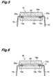
- Fig. 5 is a sectional view showing a second embodiment of the optical module. This drawing corresponds to the sectional view, shown in Fig. 4, of the first embodiment taken along the line I-I.
- no auxiliary member 30 is used for reducing the difference in thickness of the encapsulating resin, but the connecting portions 8a and 10a are formed so as to be offset to the lower side as viewed from the lead frame 2, whereby the difference in thickness between the upper and lower encapsulating resins 18a, 18b is reduced.
- the connecting portions 8a and 10a which are the respective end portions of the lead pins 8 and 10 on the wiring substrate 20 side, are bent so as to fall down from the lead frame 2.
- the position of the wiring substrate 20, shifted upward within the electronic circuit encapsulating portion 18 as shown in Fig. 4 is adjusted toward the center side, the difference in thickness between the upper and lower encapsulating resins 18a, 18b is lowered, whereby the stress is suppressed.
- Fig. 6 is a sectional view showing a third embodiment of the optical module.
- the thickness of the upper encapsulating resin 18a (including the thickness of the wiring substrate 20) from the upper surface of the lead frame 2 to the outer surface of the resin is made greater than the thickness of the lower encapsulating resin 18b from the lower surface of the lead frame 2 to the outer surface of the resin.
- the difference of encapsulating resin thickness between the upper and lower encapsulating resins 18a, 18b is compensated, whereby the stress is suppressed.
- the thickness condition concerning the upper encapsulating resin 18a and lower encapsulating resin 18b for reducing the difference in thickness therebetween may not necessarily be applied to the whole encapsulating resin forming the electronic circuit encapsulating portion 18.
- a configuration in which the above-mentioned thickness condition is applied to, of the encapsulating resin of the electronic circuit encapsulating portion 18, the part facing the wiring substrate 20 and including a portion generating a structural asymmetry within the encapsulating portion 18 can also suppress the occurrence of stress.
- Fig. 7 is a sectional view showing a fourth embodiment which is a modified example of the third embodiment shown in Fig. 6.
- a protrusion 18c with an increased thickness is formed in a part of the upper encapsulating resin 18a including the upper part of the wiring substrate 20.
- Fig. 8 is a sectional view showing a fifth embodiment which is a modified example of the third embodiment shown in Fig. 6.
- a depression 18d with a decreased thickness is formed in a part of the lower encapsulating resin 18b including the lower part of the wiring substrate 20.
- the difference in thickness between the upper and lower encapsulating resins 18a, 18b is reduced, whereby the stress is suppressed.
- each of the above-mentioned embodiments relates to a DIP type optical module
- the optical module in accordance with the present invention is similarly applicable to SIP (single inline package) type optical modules as well.
Landscapes
- Physics & Mathematics (AREA)
- General Physics & Mathematics (AREA)
- Optics & Photonics (AREA)
- Light Receiving Elements (AREA)
- Led Device Packages (AREA)
Applications Claiming Priority (2)
| Application Number | Priority Date | Filing Date | Title |
|---|---|---|---|
| JP36268498 | 1998-12-21 | ||
| JP36268498 | 1998-12-21 |
Publications (2)
| Publication Number | Publication Date |
|---|---|
| EP1014132A2 true EP1014132A2 (de) | 2000-06-28 |
| EP1014132A3 EP1014132A3 (de) | 2004-09-08 |
Family
ID=18477490
Family Applications (1)
| Application Number | Title | Priority Date | Filing Date |
|---|---|---|---|
| EP19990125511 Withdrawn EP1014132A3 (de) | 1998-12-21 | 1999-12-21 | Optisches Modul |
Country Status (2)
| Country | Link |
|---|---|
| US (1) | US6315465B1 (de) |
| EP (1) | EP1014132A3 (de) |
Families Citing this family (9)
| Publication number | Priority date | Publication date | Assignee | Title |
|---|---|---|---|---|
| SE514393C2 (sv) * | 1999-06-30 | 2001-02-19 | Ericsson Telefon Ab L M | Kapslad optomodul |
| US6780053B1 (en) * | 2000-08-09 | 2004-08-24 | Picolight Incorporated | Pluggable small form factor transceivers |
| TW490826B (en) * | 2001-05-02 | 2002-06-11 | Siliconware Precision Industries Co Ltd | Semiconductor package device and its manufacture method |
| US6827505B2 (en) * | 2002-12-16 | 2004-12-07 | International Business Machines Corporation | Optoelectronic package structure and process for planar passive optical and optoelectronic devices |
| JP2008300554A (ja) * | 2007-05-30 | 2008-12-11 | Nec Electronics Corp | 半導体装置 |
| JP2012069764A (ja) | 2010-09-24 | 2012-04-05 | On Semiconductor Trading Ltd | 回路装置およびその製造方法 |
| KR20140146612A (ko) * | 2012-04-16 | 2014-12-26 | 휴렛-팩커드 디벨롭먼트 컴퍼니, 엘.피. | 집적 광 서브-어셈블리 |
| FR3028050B1 (fr) * | 2014-10-29 | 2016-12-30 | Commissariat Energie Atomique | Substrat pre-structure pour la realisation de composants photoniques, circuit photonique et procede de fabrication associes |
| CN114709712B (zh) * | 2022-03-31 | 2025-05-13 | 广东工业大学 | 一种尺寸可调的半导体激光器烧结夹具 |
Family Cites Families (8)
| Publication number | Priority date | Publication date | Assignee | Title |
|---|---|---|---|---|
| GB2126795B (en) * | 1982-09-09 | 1986-12-03 | Plessey Co Plc | Optical device |
| JP2640766B2 (ja) | 1988-11-04 | 1997-08-13 | 大成建設株式会社 | レーザ変位計による2次元計測における相対角度の検出方法と装置 |
| DE69033400T2 (de) | 1990-03-13 | 2000-05-11 | Sumitomo Electric Industries, Ltd. | Optisches Modul und Verfahren zu seiner Herstellung |
| US5113466A (en) * | 1991-04-25 | 1992-05-12 | At&T Bell Laboratories | Molded optical packaging arrangement |
| JPH05245853A (ja) * | 1992-03-03 | 1993-09-24 | Sumitomo Electric Ind Ltd | 光モジュールの製造方法 |
| US5416871A (en) * | 1993-04-09 | 1995-05-16 | Sumitomo Electric Industries, Ltd. | Molded optical connector module |
| DE69723630T2 (de) * | 1996-08-26 | 2004-04-15 | Sumitomo Electric Industries, Ltd. | Optoelektronisches Modul und Verfahren zu dessen Herstellung |
| JP3087676B2 (ja) * | 1997-02-13 | 2000-09-11 | 日本電気株式会社 | ゲル状樹脂を用いた光結合系及び実装構造 |
-
1999
- 1999-12-20 US US09/466,926 patent/US6315465B1/en not_active Expired - Fee Related
- 1999-12-21 EP EP19990125511 patent/EP1014132A3/de not_active Withdrawn
Also Published As
| Publication number | Publication date |
|---|---|
| EP1014132A3 (de) | 2004-09-08 |
| US6315465B1 (en) | 2001-11-13 |
Similar Documents
| Publication | Publication Date | Title |
|---|---|---|
| JP3803596B2 (ja) | パッケージ型半導体装置 | |
| JP4425936B2 (ja) | 光モジュール | |
| EP0704731B1 (de) | Optisches Halbleitermodul und Verfahren zu seiner Herstellung | |
| US6467972B2 (en) | Optical interconnection module | |
| US5559918A (en) | Optical semiconductor module in which a hermetically sealed optical semiconductor device is connected to an electrical wiring layer | |
| EP1022822B1 (de) | Optisches Modul | |
| US20070221931A1 (en) | Optoelectronic semiconductor device and light signal input/output device | |
| JP2002534813A (ja) | 光子装置の密閉封止方法と装置 | |
| JP7300625B2 (ja) | 半導体装置の実装構造、光モジュール、及び半導体装置の実装構造の製造方法 | |
| US5170453A (en) | Optical module | |
| US6315465B1 (en) | Optical module | |
| US7146106B2 (en) | Optic semiconductor module and manufacturing method | |
| JP5094636B2 (ja) | 光電気配線用パッケージ | |
| US6827505B2 (en) | Optoelectronic package structure and process for planar passive optical and optoelectronic devices | |
| TW569053B (en) | Techniques for attaching rotated photonic devices to an optical sub-assembly in an optoelectronic package | |
| TWI507752B (zh) | 光學元件封裝結構 | |
| US6507035B1 (en) | Photocoupler device, method for fabricating the same, and lead frame for photocoupler device | |
| JP4104889B2 (ja) | 光半導体装置 | |
| JP4798863B2 (ja) | 光電気配線基板 | |
| JP2001343561A (ja) | 光モジュール | |
| JP2001007352A (ja) | 光・電気混載モジュール | |
| JP2000243981A (ja) | 光モジュール | |
| JP2000031582A (ja) | 光モジュール | |
| JP2927602B2 (ja) | 光結合装置 | |
| JP2000188372A (ja) | 光モジュール |
Legal Events
| Date | Code | Title | Description |
|---|---|---|---|
| PUAI | Public reference made under article 153(3) epc to a published international application that has entered the european phase |
Free format text: ORIGINAL CODE: 0009012 |
|
| AK | Designated contracting states |
Kind code of ref document: A2 Designated state(s): AT BE CH CY DE DK ES FI FR GB GR IE IT LI LU MC NL PT SE |
|
| AX | Request for extension of the european patent |
Free format text: AL;LT;LV;MK;RO;SI |
|
| PUAL | Search report despatched |
Free format text: ORIGINAL CODE: 0009013 |
|
| RIC1 | Information provided on ipc code assigned before grant |
Ipc: 7H 01S 5/022 B Ipc: 7H 01L 31/0203 B Ipc: 7G 02B 6/42 A |
|
| AK | Designated contracting states |
Kind code of ref document: A3 Designated state(s): AT BE CH CY DE DK ES FI FR GB GR IE IT LI LU MC NL PT SE |
|
| AX | Request for extension of the european patent |
Extension state: AL LT LV MK RO SI |
|
| STAA | Information on the status of an ep patent application or granted ep patent |
Free format text: STATUS: THE APPLICATION HAS BEEN WITHDRAWN |
|
| 18W | Application withdrawn |
Effective date: 20041117 |