EP1014300A1 - Kapazitive Modulation in einem elektomagnetischen Transponder - Google Patents
Kapazitive Modulation in einem elektomagnetischen Transponder Download PDFInfo
- Publication number
- EP1014300A1 EP1014300A1 EP99410180A EP99410180A EP1014300A1 EP 1014300 A1 EP1014300 A1 EP 1014300A1 EP 99410180 A EP99410180 A EP 99410180A EP 99410180 A EP99410180 A EP 99410180A EP 1014300 A1 EP1014300 A1 EP 1014300A1
- Authority
- EP
- European Patent Office
- Prior art keywords
- transponder
- modulation
- circuit
- terminal
- electronic circuit
- Prior art date
- Legal status (The legal status is an assumption and is not a legal conclusion. Google has not performed a legal analysis and makes no representation as to the accuracy of the status listed.)
- Granted
Links
Images

Classifications
-
- G—PHYSICS
- G06—COMPUTING OR CALCULATING; COUNTING
- G06K—GRAPHICAL DATA READING; PRESENTATION OF DATA; RECORD CARRIERS; HANDLING RECORD CARRIERS
- G06K19/00—Record carriers for use with machines and with at least a part designed to carry digital markings
- G06K19/06—Record carriers for use with machines and with at least a part designed to carry digital markings characterised by the kind of the digital marking, e.g. shape, nature, code
- G06K19/067—Record carriers with conductive marks, printed circuits or semiconductor circuit elements, e.g. credit or identity cards also with resonating or responding marks without active components
- G06K19/07—Record carriers with conductive marks, printed circuits or semiconductor circuit elements, e.g. credit or identity cards also with resonating or responding marks without active components with integrated circuit chips
- G06K19/077—Constructional details, e.g. mounting of circuits in the carrier
- G06K19/07749—Constructional details, e.g. mounting of circuits in the carrier the record carrier being capable of non-contact communication, e.g. constructional details of the antenna of a non-contact smart card
- G06K19/07773—Antenna details
- G06K19/07777—Antenna details the antenna being of the inductive type
-
- G—PHYSICS
- G06—COMPUTING OR CALCULATING; COUNTING
- G06K—GRAPHICAL DATA READING; PRESENTATION OF DATA; RECORD CARRIERS; HANDLING RECORD CARRIERS
- G06K19/00—Record carriers for use with machines and with at least a part designed to carry digital markings
- G06K19/06—Record carriers for use with machines and with at least a part designed to carry digital markings characterised by the kind of the digital marking, e.g. shape, nature, code
- G06K19/067—Record carriers with conductive marks, printed circuits or semiconductor circuit elements, e.g. credit or identity cards also with resonating or responding marks without active components
- G06K19/07—Record carriers with conductive marks, printed circuits or semiconductor circuit elements, e.g. credit or identity cards also with resonating or responding marks without active components with integrated circuit chips
- G06K19/0723—Record carriers with conductive marks, printed circuits or semiconductor circuit elements, e.g. credit or identity cards also with resonating or responding marks without active components with integrated circuit chips the record carrier comprising an arrangement for non-contact communication, e.g. wireless communication circuits on transponder cards, non-contact smart cards or RFIDs
Definitions
- the present invention relates to the field of transponders electromagnetic, i.e. transceivers (generally mobile) likely to be questioned without contact and wireless by a unit (generally fixed), called reading terminal and writing.
- the present invention relates, more particularly, transponders without autonomous power supply, that is to say which extract the power necessary for the circuits radiated high frequency field by an antenna of the read and write unit.
- the invention applies to such transponders, whether they are transponders read-only, i.e. suitable for operation with a terminal simply reading the data from the transponder, or read-write transponders whose data they contain can be modified by the terminal.
- the electromagnetic transponders are based on the use of oscillating circuits, transponder side and unit side read-write. These circuits are intended to be coupled by near magnetic field when the transponder enters the read-write unit field.
- the scope of a system to transponder i.e. the maximum distance from the terminal to which a transponder is activated (awake) depends, in particular, the size of the transponder antenna, the excitation frequency of the coil of the oscillating circuit generating the field magnetic, and the intensity of this excitation.
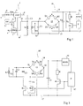
- FIG. 1 very schematically represents a classic example of a data exchange system between a unit 1 read-write and a transponder 10.
- unit 1 is essentially made up of an oscillating circuit formed by an inductor L1 in series with a capacitor C1 between an output terminal 2 of an antenna coupler 3 (COUP) and a terminal 4 at a reference potential (generally, the mass).
- the coupler 3 receives a signal fl from a oscillator 5 (OSC) and constituting a high frequency carrier.
- the signal f1 is used, in the absence of data transmission from the terminal 1 to transponder 10, from "energy source” to activate the transponder 10 if it goes into the field.
- a modulator 6 delivers a data signal data from data to be transmitted, received from an input e and coming from an electronic system (not shown).
- the midpoint of the series association of the capacitor C1 with inductance L1 constitutes, in the example shown in FIG. 1, an rx terminal for sampling a data signal, received from a transponder 10 to a demodulator 7 (DEM).
- An output s of the demodulator communicates the data received from the transponder 10 to the electronic system of the read-write unit.
- the demodulator 7 receives a signal from the oscillator 5 f2 (most often of the same frequency as the signal f1) for allow demodulation. If necessary, demodulation is made from a signal taken from the coupler terminals antenna 3 and not across the inductor L1.
- the inductance L1 of unit 1 By excitation by means of the signal f1, the inductance L1 of unit 1 generates a low intensity high frequency field.
- Transponder side 10 an L2 choke, in parallel with a capacitor C2, forms an oscillating circuit (called circuit resonating in reception) parallel and intended to capture the field generated by the oscillating circuit of unit 1.
- the resonant circuit (L2, C2) of transponder 10 is tuned to the frequency of oscillating circuit (L1, C1) of unit 1.
- Terminals 11, 12 of the resonant circuit are connected to two input terminals alternative of a righting bridge 13 constituted, by example, of four diodes D1, D2, D3, D4.
- the anode of the diode Dl is connected to the terminal 11, as well as the cathode of diode D3.
- the anode of diode D2 and the cathode of diode D4 are connected to terminal 12.
- the cathodes of diodes D1 and D2 constitute a positive terminal 14 of straightened outlet.
- the anodes of diodes D3 and D4 constitute a reference terminal 15 of the rectified voltage.
- a Ca capacitor is connected in parallel with the rectified output terminals 14, 15 of bridge 13 so as to filter the rectified voltage delivered by the bridge.
- transponder 10 When transponder 10 is in the field of unit 1, a high frequency voltage is generated at the terminals of the resonant circuit. This voltage, rectified by bridge 13 and smoothed by the capacitor Ca, provides a supply voltage Goes to electronic transponder circuits via of a voltage regulator 16 (BACKUP). Electronic circuits of the transponder have been symbolized in FIG. 1 by a block 17 (P). It is generally a chip (integrating the most often the regulator 16) containing at least one memory and one processor.
- block 17 controls a modulation stage (retromodulation) of the resonant circuit (L2, C2).
- This modulation stage usually consists of an electronic switch (a transistor 18) and a resistor R, associated in series between the terminals 14 and 15.
- the transistor 18 is controlled at a frequency significantly lower (usually with a ratio of at least 10) with respect to the frequency f1 of the circuit excitation signal oscillating unit 1.
- the oscillating circuit of the transponder is therefore subject to additional depreciation compared to the load consisting of regulator 16 and circuit 17 when the switch 18 is closed. The voltage drops across the winding L2 so that the transponder takes a quantity of energy higher in the high frequency field.
- Another method is to detect the variation of phase due to this change in load on the oscillating circuit of unit 1.
- amplitude modulation representing, or the entire amplitude of the signal f1, (modulation all or nothing), or a small portion (of the order of 10%) of this amplitude due to the power requirement of the transponder 10.
- the modulation is transmitted digitally, by jumping between two binary levels.
- the tuning frequency of the oscillating circuits conditions the transmission rate as far as the frequency modulation, via switch 18 on the transponder side, must be significantly lower than the carrier frequency used to supply power to the transponders. Therefore, the higher the feed carrier frequency, the higher the flow can be important.
- the frequency of the carrier fl is 13.56 MHz and the frequency of the switch control pulses 18, transponder side, is 847 kHz (16 times less).
- a first drawback is that there are “transmission holes”, that is, distances between the transponder and the terminal at which the latter does not detect the transponder even when it is in its field. These transmission holes occur when the transponder is very close to the read-write unit, i.e. when the distance between the two coupling elements L1 and L2 inductive is low compared to the operating range of the system. For example, for application to systems with low distance at a frequency of 13.56 MHz, the range is the order of 10 centimeters and we see appear losses of detection when the transponder is less than three centimeters of the read-write unit.
- a classic solution to solve this problem is to force a minimum gap between the transponder and unit 1.
- a disadvantage of such a solution is that it reduces the scope of the system.
- transponder systems classics Another disadvantage of transponder systems classics is that the use of a resistance R in the stage of modulation of the transponder 10 causes dissipation during the modulation by the transponder. Now, as mentioned earlier, the transponder is not powered independently but draws its power from the high frequency field from of the read-write system. Therefore, any consumption energy should be minimized.
- An object of the present invention is to overcome the disadvantages of conventional transponder systems.
- the present invention aims, in particular, to propose a new transponder architecture that avoids "holes" transmission while preserving the maximum range of reach at system.
- the present invention also aims to provide a solution that is particularly simple to implement and economical from the point of view of the components used, so as to favor miniaturization of the transponder.
- the present invention further aims to minimize the energy consumption of the transponder.
- the solution recommended by the present invention is to use, on the transponder side, an active modulation element on the resonant frequency of the oscillating circuit and not on its amplitude as in the case of a resistance. So this invention proposes to slightly detune the oscillating circuits during modulation (retromodulation) by the transponder.
- the present invention originates from a new analysis of the causes of transmission losses in systems with electromagnetic transponders.
- FIG. 2 represents, for several deviations between a transponder and a read-write unit, examples of voltage-frequency characteristics, where the voltage represents the remote supply voltage of the transponder, for example, the voltage V2 at the terminals of the inductor L2 of the transponder, and where f corresponds to the excitation frequency of the terminal's oscillating circuit.
- the different curves illustrated in Figure 2 are plotted for oscillating circuits tuned to position fi, that is to say the resonance frequency of the circuits L1, C1 and L2, C2.
- the curves g1, g2, g3, g4, g5 and g6 indicate distances decreasing between the transponder and the read-write system.
- the curve g1 which represents a small dome centered on the tuning frequency fi, corresponds substantially at the system range limit.
- the curve g4 illustrates the position optimal coupling, i.e.
- the pace of the voltage as a function of frequency represents, for these distances, two peaks on either side of the tuning frequency linked one to the other by a minimum (hole) at the tuning frequency.
- the more the distance decreases the more the two peaks deviate from each other and the lower the minimum is close to zero voltage.
- the present invention proposes to use a modulation acting on the resonance frequency of the oscillating circuit by modifying the equivalent capacity of the oscillating circuit on the transponder side. Note that, in the absence retromodulation by transponder, oscillating circuits remain tuned, i.e. with the same frequency of resonance. So only when there is a need to transmit data from the transponder to the base which is shifted slightly the resonance frequency of the oscillating circuit of the transponder so as to leave the area of possible "holes" depending on the distance between the transponder and the terminal, and allow thus transmitting data from the transponder to the thick headed.
- the transponder is necessarily detected by the terminal insofar as, in such an electromagnetic system, the transponder necessarily starts with an approach from the far range distance to a longer distance low.
- Capacitive modulation does not disturb resonance in terms of its magnitude from the time the low value of the capacity, which is added to the capacity of the circuit resonant, maintains the coupling in an area close to the chord. Therefore, as there is no longer a resistive voltage drop additional, the remote power supply is preserved.
- Capacitive modulation directly influences the phase of the voltage across the inductance L1 of the terminal because, by coupling, this modulation is brought back on this inductance and it introduces a variation essentially on the imaginary part of the complex impedance of circuit L1, C1, therefore directly on the phase.
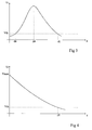
- Figures 3 and 4 illustrate, depending on the distance d (difference between the transponder and the terminal), the amplitudes Vr of the signal recovered, at output s (figure 1) on the terminal side, following retromodulations, respectively resistive and capacitive, for a system in which the oscillating circuits are (in no modulation) granted.
- FIG. 3 shows an example of a characteristic in resistive retromodulation.
- the amplitude of the retromodulation has a shape approximately in bell, centered on a gap d4 corresponding to an optimal coupling (curve g4 in Figure 2).
- the amplitude of the retromodulation is below a Vth threshold of detection by the demodulator. This corresponds to the dl limit of scope of the system.
- the amplitude is below the terminal detection threshold Vth, where the drop in voltage linked to the modulation is superimposed on a remote feed hole.
- Figure 4 shows a similar example, but for capacitive modulation.
- the shape of the amplitude-distance characteristic here has an approximately linear decrease since a maximum Vmax until passing below the detection threshold Vth when the distance reaches the system range limit dl. So the remote feed holes have no effect on capacitive retromodulation.
- a first solution would be to connect a capacitor in series with a control switch between the terminals 11 and 12, that is to say in parallel on the capacitor C2 of the oscillating circuit.
- an object of the present invention is to propose a new solution allowing a modification of the capacity equivalent of the oscillating circuit by simple means.
- the present invention aims to allow the control, by means of simple MOS transistors, of a means of capacitive modulation of the oscillating circuit of the transponder.
- the present invention also aims to ensure that it is not no need to modify the type of classic command operated at circuit means (17, figure 1) in the case of a modulation stage resistive.
- the present invention provides a electromagnetic transponder of the type comprising a circuit oscillating upstream of a rectification means capable of providing a DC supply voltage of an electronic circuit, the electronic circuit comprising means for transmitting digitally encoded information, and the transponder comprising two capacitive modulation means, respectively associated with each end terminal of the inductive element of the oscillating circuit, a reference terminal of each modulation means being connected to the circuit supply reference potential electronic, downstream of the rectifying means.
- each capacitive modulation means consists of a transistor MOS connected between one of the end terminals of the inductor of the oscillating circuit and the voltage reference terminal continuous supply of the electronic circuit, the grid each transistor receiving the modulation signal emitted by the electric circuit.
- each transistor constitutes a control switch of a capacitor with which it is associated in series, between one of end terminals of the inductive element of the oscillating circuit and the reference terminal of the electronic circuit.
- the inductive element of the oscillating circuit includes a midpoint constituting the reference potential of the electronic circuit.
- the transponder further comprises a resistive modulation means, in parallel on a voltage filtering capacitor rectified delivered by said rectifying means.
- the capacitive and resistive modulation means are controlled to from the same signal.
- the resistive modulation means is controlled through a circuit validation of the control signal of said modulation means capacitive.
- the invention also relates to a transmission system.
- electromagnetic of the type comprising a read-write terminal generating an electromagnetic field suitable for cooperation with at least one transponder when the latter enters this field.
- FIG. 5 represents a first embodiment a 10 'transponder according to the present invention.
- this transponder is made from a circuit oscillating formed by an inductance L2 and a capacitor C2 connected in parallel between two terminals 11, 12 of alternative input of a bridge 13.
- Two rectified output terminals 14, 15 of the bridge 13 provide, via a capacitor Ca filtering, a supply voltage of an electronic unit 17, for example a P processor.
- the voltage block 17 is supplied by a regulator circuit 16 (BACKUP).
- BACKUP regulator circuit 16
- the regulation illustrated as being a series type regulation can also be of type parallel to by means of a regulator connected between terminals 14 and 15.
- two capacitors of modulation C3 and C4 are each associated in series with a switch (for example, a MOS transistor) K1, K2, respectively between terminals 11 and 12 and terminal 15.
- a switch for example, a MOS transistor
- K1, K2 a MOS transistor
- a first terminal of capacitor C3 is connected to terminal 11 while that its other terminal is connected, via the transistor K1, at terminal 15.
- a first terminal of capacitor C4 is connected to terminal 12 while its other terminal is connected, via a transistor K2, to terminal 15.
- two capacities are used respectively associated with each sign of the alternating voltage V2.
- the two capacitors C3 and C4 are therefore of the same value, appropriate to perform the desired modulation.
- the two K1 transistors and K2 are controlled by block 17, preferably from a same signal.
- a feature of the present invention is that thanks to the splitting of the capacitors modulation, you can have a reference point (line 15) for controlling switches K1 and K2. So if switches K1 and K2 are made up of MOS transistors N channel, it is now possible, by a logic signal from the block 17, to control these switches all or nothing so to provide the necessary modulation to transmit data to the fixed read-write terminal.
- a retromodulation circuit resistive consisting, as for a conventional transponder, of a resistance R associated with a switch 18 in series between the terminals 14 and 15.
- R a resistance associated with a switch 18 in series between the terminals 14 and 15.
- FIG. 6 shows a second embodiment a 10 "transponder according to the present invention.
- This transponder 10 "contains substantially the same elements as those of the figure 5.
- a feature of this second embodiment is to provide an inductor L2 'at midpoint 15'. This point medium then serves as a reference line for continuous feeding of the electronic circuit on the transponder side. So, a first terminal 11 of the winding L2 'is connected to the anode of a diode rectifier Dl 'whose cathode constitutes the supply terminal 14 of the transponder side circuit. A second terminal 12 of winding L2 'is connected to the anode of a rectifying diode D4 'whose cathode is connected to terminal 14.
- the capacitor C2 is, as before, connected between terminals 11 and 12. Likewise, each modulation stage capacitive is respectively connected between terminals 11 and 15 ' and between terminals 12 and 15 '.
- a first capacitor C3, associated in series with a first switch K1 is connected between terminals 11 and 15 'while a second capacitor C4, associated in series with a second switch K2, is connected between terminals 12 and 15 '.
- the respective control terminals switches K1 and K2 (for example, the respective grids MOS transistors) are connected to an output terminal of the block electronics 17 (for example, the transponder processor).
- a filtering capacitor Ca is connected between terminals 14 and 15 'to filter the supply voltage of the electronic circuit and, in particular, supply the regulator 16.
- a resistive modulation stage consisting of a resistor R associated in series with a switch 18 between terminals 14 and 15 '. Note however that, as for the embodiment In Figure 5, this resistive modulation stage is optional.
- An advantage of the second embodiment is that two diodes are sufficient to carry out the rectification necessary for the power supply to the electronic circuit of the transponder.
- this embodiment requires a point inductor middle.
- the choice between the first and the second embodiment will depend on the application and, in particular, on the frequency of use which conditions the size of the inductor necessary.
- the modulation capacities are constituted by the intrinsic capacities of MOS transistors constituting switches K1 and K2.
- the drain / source capacitance of MOS transistors we use the drain / source capacitance of MOS transistors, so only two MOS transistors are needed.
- the capacity values required for retromodulation by the transponder are compatible with the capacities intrinsic of the MOS transistors produced. Note that the control signals must then be adapted, the capacities parasites being functionally present only when the transistors are blocked.
- the present invention is capable of various variants and modifications which will appear to the man of art.
- the respective dimensions of the capacitors, resistors and inductors, as well as other components of a transponder according to the present invention are at the scope of the skilled person depending on the application.
- the present invention finds a special interest in electromagnetic transmission systems operating at high frequency. Indeed, at such frequencies, the displacement speeds of the transponders by users are negligible compared to the transmission rate information so the electromagnetic coupling is not significantly changed during an exchange of information.
Landscapes
- Engineering & Computer Science (AREA)
- Computer Networks & Wireless Communication (AREA)
- Computer Hardware Design (AREA)
- Microelectronics & Electronic Packaging (AREA)
- Physics & Mathematics (AREA)
- General Physics & Mathematics (AREA)
- Theoretical Computer Science (AREA)
- Near-Field Transmission Systems (AREA)
- Radar Systems Or Details Thereof (AREA)
Applications Claiming Priority (2)
| Application Number | Priority Date | Filing Date | Title |
|---|---|---|---|
| FR9816383 | 1998-12-21 | ||
| FR9816383A FR2787655B1 (fr) | 1998-12-21 | 1998-12-21 | Modulation capacitive dans un transpondeur electromagnetique |
Publications (2)
| Publication Number | Publication Date |
|---|---|
| EP1014300A1 true EP1014300A1 (de) | 2000-06-28 |
| EP1014300B1 EP1014300B1 (de) | 2007-07-04 |
Family
ID=9534452
Family Applications (1)
| Application Number | Title | Priority Date | Filing Date |
|---|---|---|---|
| EP99410180A Expired - Lifetime EP1014300B1 (de) | 1998-12-21 | 1999-12-20 | Kapazitive Modulation in einem elektromagnetischen Transponder |
Country Status (5)
| Country | Link |
|---|---|
| US (1) | US6356198B1 (de) |
| EP (1) | EP1014300B1 (de) |
| JP (1) | JP4332963B2 (de) |
| DE (1) | DE69936439T2 (de) |
| FR (1) | FR2787655B1 (de) |
Cited By (1)
| Publication number | Priority date | Publication date | Assignee | Title |
|---|---|---|---|---|
| EP1267303B1 (de) * | 2001-06-11 | 2011-07-27 | HID Global GmbH | Transponder |
Families Citing this family (21)
| Publication number | Priority date | Publication date | Assignee | Title |
|---|---|---|---|---|
| DE10004922A1 (de) * | 2000-02-04 | 2001-08-09 | Giesecke & Devrient Gmbh | Transponder, insbesondere für eine kontaktlose Chipkarte |
| FR2808634A1 (fr) * | 2000-05-05 | 2001-11-09 | St Microelectronics Sa | Amelioration de la capacite de demodulation d'un transpondeur electromagnetique |
| EP1474776B1 (de) * | 2002-02-01 | 2008-11-26 | Nxp B.V. | Anpassung der spulenspannung eines transponders an die feldstärke |
| US20050012597A1 (en) * | 2003-07-02 | 2005-01-20 | Anderson Peter Traneus | Wireless electromagnetic tracking system using a nonlinear passive transponder |
| EP1538557B1 (de) * | 2003-12-05 | 2013-02-13 | STMicroelectronics S.A. | Widerstands- und Kapazitätsmodulation in einem elektromagnetischen Transponder |
| TWI315493B (en) * | 2006-08-03 | 2009-10-01 | Holtek Semiconductor Inc | Transponder for rfid |
| AU2008339692B2 (en) | 2007-12-21 | 2014-08-21 | Access Business Group International Llc | Circuitry for inductive power transfer |
| FR2947075A1 (fr) | 2009-06-19 | 2010-12-24 | St Microelectronics Rousset | Evaluation resistive du facteur de couplage d'un transpondeur electromagnetique |
| JP5443650B2 (ja) * | 2010-04-06 | 2014-03-19 | ヴェーデクス・アクティーセルスカプ | モニタリング装置,およびモニタリング装置における無線データおよび電力の送信方法 |
| WO2012149869A1 (zh) * | 2011-05-03 | 2012-11-08 | 国民技术股份有限公司 | 一种通信方法、通信装置及通信系统 |
| FR2976102B1 (fr) | 2011-06-03 | 2013-05-17 | St Microelectronics Rousset | Assistance au positionnement d'un transpondeur |
| FR2976105B1 (fr) | 2011-06-03 | 2013-05-17 | St Microelectronics Rousset | Securisation d'une communication par un transpondeur electromagnetique |
| FR2976103B1 (fr) | 2011-06-03 | 2013-05-17 | St Microelectronics Rousset | Aide au positionnement d'un transpondeur |
| FR2976104B1 (fr) | 2011-06-03 | 2013-11-15 | St Microelectronics Rousset | Securisation d'une communication entre un transpondeur electromagnetique et un terminal |
| KR102022867B1 (ko) | 2012-08-07 | 2019-09-20 | 삼성전자 주식회사 | Nfc 회로 및 이의 동작 방법 |
| CN103714378B (zh) * | 2014-01-08 | 2016-09-07 | 卓捷创芯科技(深圳)有限公司 | 一种无源射频标签的智能化能量管理系统与能量管理方法 |
| CN103679259B (zh) * | 2014-01-08 | 2016-08-17 | 卓捷创芯科技(深圳)有限公司 | 一种具有多种时间常数的整流限幅电路和无源射频标签 |
| US10608471B2 (en) * | 2016-09-16 | 2020-03-31 | Integrated Device Technology, Inc. | Multimode wireless power receiver circuit |
| US10224757B2 (en) | 2016-12-28 | 2019-03-05 | Texas Instruments Incorporated | Methods and apparatus for antenna signal limiter for radio frequency identification transponder |
| US10038579B1 (en) * | 2017-03-15 | 2018-07-31 | Texas Instruments Incorporated | Integrated circuits and transponder circuitry with shared modulation capacitor for 3D transponder uplink modulation |
| DE102024200553A1 (de) * | 2024-01-22 | 2025-07-24 | Fraunhofer-Gesellschaft zur Förderung der angewandten Forschung eingetragener Verein | Modulationsschaltung |
Citations (2)
| Publication number | Priority date | Publication date | Assignee | Title |
|---|---|---|---|---|
| US5287112A (en) * | 1993-04-14 | 1994-02-15 | Texas Instruments Incorporated | High speed read/write AVI system |
| WO1998011504A1 (de) * | 1996-09-12 | 1998-03-19 | Fraunhofer-Gesellschaft zur Förderung der angewandten Forschung e.V. | Passiver transponder |
Family Cites Families (20)
| Publication number | Priority date | Publication date | Assignee | Title |
|---|---|---|---|---|
| WO1993011509A1 (fr) * | 1991-12-04 | 1993-06-10 | Citizen Watch Co., Ltd. | Support de donnees |
| US4075632A (en) * | 1974-08-27 | 1978-02-21 | The United States Of America As Represented By The United States Department Of Energy | Interrogation, and detection system |
| US4580041A (en) * | 1983-12-09 | 1986-04-01 | Walton Charles A | Electronic proximity identification system with simplified low power identifier |
| NL8701565A (nl) * | 1987-07-03 | 1989-02-01 | Nedap Nv | Identificatiesysteem met twee werkingsmodes. |
| NL8702426A (nl) * | 1987-10-12 | 1989-05-01 | Nedap Nv | Werkwijze en inrichting voor het identificeren van metalen pallets en containers. |
| US5701121A (en) * | 1988-04-11 | 1997-12-23 | Uniscan Ltd. | Transducer and interrogator device |
| US5099228A (en) * | 1989-02-09 | 1992-03-24 | Marcia Israel | Electronic anti-theft merchandise tag having means for activating an alarm in response to an attempt to remove the tag from the merchandise |
| US5214409A (en) * | 1991-12-03 | 1993-05-25 | Avid Corporation | Multi-memory electronic identification tag |
| DE4327642C2 (de) * | 1993-05-17 | 1998-09-24 | Anatoli Stobbe | Lesegerät für ein Detektierplättchen |
| US5347280A (en) * | 1993-07-02 | 1994-09-13 | Texas Instruments Deutschland Gmbh | Frequency diversity transponder arrangement |
| US5446447A (en) * | 1994-02-16 | 1995-08-29 | Motorola, Inc. | RF tagging system including RF tags with variable frequency resonant circuits |
| WO1997004201A1 (de) * | 1995-07-24 | 1997-02-06 | Siemens Aktiengesellschaft | Diebstahlschutzsystem für ein kraftfahrzeug |
| US5625341A (en) * | 1995-08-31 | 1997-04-29 | Sensormatic Electronics Corporation | Multi-bit EAS marker powered by interrogation signal in the eight MHz band |
| FR2741978B1 (fr) * | 1995-12-01 | 1998-01-23 | Pierre Raimbault | Circuit d'alimentation et de modulation pour une etiquette interrogeable a distance |
| US6167094A (en) * | 1996-10-15 | 2000-12-26 | Siemens Aktiengesellschaft | Data transmission circuit having a station and a response circuit |
| US5883582A (en) * | 1997-02-07 | 1999-03-16 | Checkpoint Systems, Inc. | Anticollision protocol for reading multiple RFID tags |
| US6208235B1 (en) * | 1997-03-24 | 2001-03-27 | Checkpoint Systems, Inc. | Apparatus for magnetically decoupling an RFID tag |
| ITTO980146A1 (it) * | 1998-02-25 | 1999-08-25 | Alessandro Manneschi | Sistema rivelatore per controllo di accesso e relativo gruppo rivela- tore. |
| US6072383A (en) * | 1998-11-04 | 2000-06-06 | Checkpoint Systems, Inc. | RFID tag having parallel resonant circuit for magnetically decoupling tag from its environment |
| US6054625A (en) * | 1999-05-27 | 2000-04-25 | Witco Corporation | Heteropolyacids as catalysts for a synthesis of ketone peroxides |
-
1998
- 1998-12-21 FR FR9816383A patent/FR2787655B1/fr not_active Expired - Fee Related
-
1999
- 1999-12-20 JP JP36095499A patent/JP4332963B2/ja not_active Expired - Lifetime
- 1999-12-20 EP EP99410180A patent/EP1014300B1/de not_active Expired - Lifetime
- 1999-12-20 US US09/467,603 patent/US6356198B1/en not_active Expired - Lifetime
- 1999-12-20 DE DE69936439T patent/DE69936439T2/de not_active Expired - Lifetime
Patent Citations (2)
| Publication number | Priority date | Publication date | Assignee | Title |
|---|---|---|---|---|
| US5287112A (en) * | 1993-04-14 | 1994-02-15 | Texas Instruments Incorporated | High speed read/write AVI system |
| WO1998011504A1 (de) * | 1996-09-12 | 1998-03-19 | Fraunhofer-Gesellschaft zur Förderung der angewandten Forschung e.V. | Passiver transponder |
Cited By (1)
| Publication number | Priority date | Publication date | Assignee | Title |
|---|---|---|---|---|
| EP1267303B1 (de) * | 2001-06-11 | 2011-07-27 | HID Global GmbH | Transponder |
Also Published As
| Publication number | Publication date |
|---|---|
| DE69936439T2 (de) | 2008-03-13 |
| DE69936439D1 (de) | 2007-08-16 |
| US6356198B1 (en) | 2002-03-12 |
| FR2787655B1 (fr) | 2001-03-09 |
| FR2787655A1 (fr) | 2000-06-23 |
| EP1014300B1 (de) | 2007-07-04 |
| JP4332963B2 (ja) | 2009-09-16 |
| JP2000228637A (ja) | 2000-08-15 |
Similar Documents
| Publication | Publication Date | Title |
|---|---|---|
| EP1014300B1 (de) | Kapazitive Modulation in einem elektromagnetischen Transponder | |
| EP1045336B1 (de) | Enggekoppeltes Betriebsverfahren eines elektromagnetischen Transpondersystem | |
| EP1045325B1 (de) | Entfernungsbestimmung zwischen einem elektromagnetischen Transponder und einem Terminal | |
| EP1043680B1 (de) | Enggekoppelter elektromagnetischer Transponder | |
| EP1617550B1 (de) | Adaptierbare Stromversorgung | |
| EP1043677B1 (de) | Ein mit sehr naher Koppelung arbeitendes Lesegerät für elektromagnetische Transponder | |
| WO1998026371A1 (fr) | Systeme d'echange de donnees a communication par contacts ou sans contact entre une borne et des objets portatifs | |
| FR2768880A1 (fr) | Demodulateur pour carte a puce sans contact | |
| EP1445877B1 (de) | Kommunikation zwischen elektromagnetischen Transpondern | |
| EP1610257A1 (de) | Impedanzanpassung in einem Gerät zum Lesen elektromagnetischer Transpondern | |
| EP1043679B1 (de) | Leser mit Einrichtung zur Bestimmung des Abstandes zwischen dem Leser und einem Transponder | |
| EP1043678B1 (de) | Duplexübertragung in einem elektromagnetischen Transponder-System | |
| EP2107694A1 (de) | Endgerät zur Funksendung und zum Funkempfang durch induktive Kupplung | |
| FR2840742A1 (fr) | Lecteur de transpondeur electromagnetique | |
| FR2796782A1 (fr) | Dimensionnement d'un systeme a transpondeur electromagnetique pour un fonctionnement dedie en couplage lointain | |
| EP1163734B1 (de) | Schaltungsanordnung zum empfangen und senden von daten mit induktiver kopplung | |
| EP1071039A1 (de) | Auslegung eines elektromagnetischen Transponder-Systems für Nahübertragung | |
| EP1672388B1 (de) | Elektromagnetischer Transponder ohne eigenständige Energieversorgung | |
| EP3012980A1 (de) | Verfahren zur steuerung des betriebs, insbesondere der belastungsmodulation, eines objekts, das in der lage ist, kontaktlos mit einem lesegerät zu kommunizieren, entsprechende vorrichtung und entsprechendes objekt | |
| FR2808634A1 (fr) | Amelioration de la capacite de demodulation d'un transpondeur electromagnetique | |
| EP1163718B1 (de) | Verfahren zum modulieren der amplitude eines signals und dessen ausstrahlung durch eine antenne | |
| EP1196926B1 (de) | Spannungserzeugungsschaltung für smart card | |
| US20050175118A1 (en) | Data carrier comprising means for influencing the slope course of the signal edges in an amplitude-modulated signal | |
| EP1039408A1 (de) | Fernspeisung für einen elektromagnetischen Transponder | |
| FR2792133A1 (fr) | Regulation de phase d'un lecteur de transpondeurs electromagnetiques |
Legal Events
| Date | Code | Title | Description |
|---|---|---|---|
| PUAI | Public reference made under article 153(3) epc to a published international application that has entered the european phase |
Free format text: ORIGINAL CODE: 0009012 |
|
| AK | Designated contracting states |
Kind code of ref document: A1 Designated state(s): DE FR GB IT |
|
| AX | Request for extension of the european patent |
Free format text: AL;LT;LV;MK;RO;SI |
|
| 17P | Request for examination filed |
Effective date: 20001215 |
|
| AKX | Designation fees paid |
Free format text: DE FR GB IT |
|
| RAP1 | Party data changed (applicant data changed or rights of an application transferred) |
Owner name: STMICROELECTRONICS S.A. |
|
| GRAP | Despatch of communication of intention to grant a patent |
Free format text: ORIGINAL CODE: EPIDOSNIGR1 |
|
| GRAS | Grant fee paid |
Free format text: ORIGINAL CODE: EPIDOSNIGR3 |
|
| GRAA | (expected) grant |
Free format text: ORIGINAL CODE: 0009210 |
|
| AK | Designated contracting states |
Kind code of ref document: B1 Designated state(s): DE FR GB IT |
|
| REG | Reference to a national code |
Ref country code: GB Ref legal event code: FG4D Free format text: NOT ENGLISH |
|
| REF | Corresponds to: |
Ref document number: 69936439 Country of ref document: DE Date of ref document: 20070816 Kind code of ref document: P |
|
| GBT | Gb: translation of ep patent filed (gb section 77(6)(a)/1977) |
Effective date: 20070917 |
|
| PLBE | No opposition filed within time limit |
Free format text: ORIGINAL CODE: 0009261 |
|
| STAA | Information on the status of an ep patent application or granted ep patent |
Free format text: STATUS: NO OPPOSITION FILED WITHIN TIME LIMIT |
|
| 26N | No opposition filed |
Effective date: 20080407 |
|
| REG | Reference to a national code |
Ref country code: FR Ref legal event code: PLFP Year of fee payment: 17 |
|
| REG | Reference to a national code |
Ref country code: FR Ref legal event code: PLFP Year of fee payment: 18 |
|
| REG | Reference to a national code |
Ref country code: FR Ref legal event code: PLFP Year of fee payment: 19 |
|
| PGFP | Annual fee paid to national office [announced via postgrant information from national office to epo] |
Ref country code: DE Payment date: 20181126 Year of fee payment: 20 |
|
| PGFP | Annual fee paid to national office [announced via postgrant information from national office to epo] |
Ref country code: IT Payment date: 20181122 Year of fee payment: 20 Ref country code: FR Payment date: 20181127 Year of fee payment: 20 Ref country code: GB Payment date: 20181127 Year of fee payment: 20 |
|
| REG | Reference to a national code |
Ref country code: DE Ref legal event code: R071 Ref document number: 69936439 Country of ref document: DE |
|
| REG | Reference to a national code |
Ref country code: GB Ref legal event code: PE20 Expiry date: 20191219 |
|
| PG25 | Lapsed in a contracting state [announced via postgrant information from national office to epo] |
Ref country code: GB Free format text: LAPSE BECAUSE OF EXPIRATION OF PROTECTION Effective date: 20191219 |