EP1014567A2 - Verbesserungen an oder in Bezug auf einen Operationsverstärker - Google Patents
Verbesserungen an oder in Bezug auf einen Operationsverstärker Download PDFInfo
- Publication number
- EP1014567A2 EP1014567A2 EP99204415A EP99204415A EP1014567A2 EP 1014567 A2 EP1014567 A2 EP 1014567A2 EP 99204415 A EP99204415 A EP 99204415A EP 99204415 A EP99204415 A EP 99204415A EP 1014567 A2 EP1014567 A2 EP 1014567A2
- Authority
- EP
- European Patent Office
- Prior art keywords
- current
- coupled
- transistor
- circuit
- guiding region
- Prior art date
- Legal status (The legal status is an assumption and is not a legal conclusion. Google has not performed a legal analysis and makes no representation as to the accuracy of the status listed.)
- Granted
Links
Images


Classifications
-
- H—ELECTRICITY
- H03—ELECTRONIC CIRCUITRY
- H03F—AMPLIFIERS
- H03F1/00—Details of amplifiers with only discharge tubes, only semiconductor devices or only unspecified devices as amplifying elements
- H03F1/32—Modifications of amplifiers to reduce non-linear distortion
- H03F1/3217—Modifications of amplifiers to reduce non-linear distortion in single ended push-pull amplifiers
-
- H—ELECTRICITY
- H03—ELECTRONIC CIRCUITRY
- H03F—AMPLIFIERS
- H03F3/00—Amplifiers with only discharge tubes or only semiconductor devices as amplifying elements
- H03F3/30—Single-ended push-pull [SEPP] amplifiers; Phase-splitters therefor
- H03F3/3083—Single-ended push-pull [SEPP] amplifiers; Phase-splitters therefor the power transistors being of the same type
- H03F3/3086—Single-ended push-pull [SEPP] amplifiers; Phase-splitters therefor the power transistors being of the same type two power transistors being controlled by the input signal
- H03F3/3088—Single-ended push-pull [SEPP] amplifiers; Phase-splitters therefor the power transistors being of the same type two power transistors being controlled by the input signal with asymmetric control, i.e. one control branch containing a supplementary phase inverting transistor
Definitions
- This invention relates generally to the field of operational amplifiers; and, in particular, to an output stage and method having a latchup-free sourcing current booster capable of driving low impedance loads.
- the operational amplifier consists of at least two stages: an input amplifier stage and an output stage.
- the input amplifier stage has the task of deriving the difference between the two inputs.
- the primary purpose of the output stage is voltage amplification.
- the output stage optionally has some sort of current boosting scheme which increases the amplifier's load capacity.
- amplifier output stages have used techniques involving combinations of transistors including npn, pnp and metal oxide semiconductor field effect transistors to satisfy many performance specifications, such as low crossover distortion, large output voltage swings including rail to rail performance, excellent phase and gain margins, low output impedance and symmetrical source and sink capabilities.
- a well-designed output stage should achieve these performance specifications while consuming low quiescent power and not limiting the frequency response of the amplifier.
- an amplifier circuit consumes current from a power supply.
- a portion of this current known as the quiescent current, is used to bias the internal circuitry of the amplifier.
- a low quiescent current is desirable because it reduces power consumption when the amplifier is operating at a light load, or with no load at all.
- FIG. 1 illustrates a conventional output stage 10.
- This circuit schematic illustrates an embodiment of a traditional Class AB output stage 10 of an operational amplifier capable of driving a specified minimum impedance load while possessing a low quiescent current.
- Current source 12 provides quiescent biasing current I Q to drive the control region of sourcing transistor 26.
- Sinking transistor 30 coupled in series with sourcing transistor 26 sinks current from the external load provided at output node 28.
- Current mirror transistor 22 has its control region and first current guiding region coupled to the control region and first current guiding region of the sinking transistor 30, respectively. In addition, the control region of current mirror transistor 22 is coupled to input 16.
- Diode 14 is coupled in series between the second current guiding region of current mirror transistor 22 and the current source 12.
- the resistor 18 is coupled between the diode 14 and the output terminal of output stage 28.
- Diode 20 is coupled in parallel with resistor 18 to provide diode-resistor current limiting. Raising the quiescent current will drive lower impedance loads. This type of design modification, however, leads to too much standby power dissipation and; thus, is inefficient.
- a current mirror circuit 44 formed by transistors 46 and 48 provides a boosting current I boost from the biasing current source 58 to drive the control region of an sourcing transistor 52.
- the first current guiding regions of both current mirror transistors 46 and 48 are coupled to a first power supply rail 42 having power V CC .
- the control regions of both current mirror transistors 46 and 48 are tied together. Accordingly, the current mirror transistor 48 has a directly coupled control region and second current guiding region.
- Resistor 50 has small resistance R coupled in parallel to the current mirror circuit 44 such that when the current of sourcing transistor 52 is small, the resistor 50 does not have any significant voltage drop across it.
- Current source 58 is coupled to the current mirror circuit 44 supplies a bias current Ibias to drive the current mirror circuit 44.
- Current I boost provided by the current mirror 44 through current mirror transistor 46 drives the sourcing transistor 52.
- Boosting current I boost approximately equals the bias current I bias.
- Current I out flows through sourcing transistor 52 to an output node 56.
- Sinking transistor 54 coupled in series with sourcing transistor 52 sinks current from the external load provided at output 56.
- Sinking transistor 54 is coupled to a input amplifier (not shown) at input node 60.
- the current in sourcing transistor 52 increases, the voltage drop across resistor 50 increases.
- the current in first current mirror transistor 46 increases exponentially with the voltage increase across resistor 50.
- first current mirror transistor 46 grows exponentially as the current in sourcing transistor 52 increases linearly, making the boosting current I boost in current mirror circuit 44 non-linear.
- transistor 52 will conduct heavily, raising the output to the power supply voltage level and causing the circuit to latch-up.
- the circuit ceases operation due to latch-up at higher output currents.
- Decreasing the value of resistance 50 in an effort to prevent the occurrence of latch-up results in decreased boosting current Iboost, which defeats the purpose of providing a current boosting scheme.
- a limitation of this particular type of topology exists such that it may be used solely with external loads having a specified limited range. This limitation exists primarily because the biasing signal of this boosting scheme has no dependence upon the input signal; yet, biases the output stage 40 control regiond upon its output signal.
- FIG. 2b illustrates another conventional amplifier design 70 which uses another boosting scheme to generate higher output current I out .
- This amplifier 70 includes an output driver having a sourcing transistor 78 coupled to sinking transistor 80 at a common output node 82.
- Transistor 76 includes a control region coupled to the input signal 74, an first current guiding region coupled to a first power supply reference 72 and a second current guiding region coupled to the control region of the sourcing transistor 78.
- Current through transistor 76 provides ample boosting current I boost for the control region of sourcing transistor 78. Accordingly, this design provides boosting current that is control regiond upon both the input signal and the output signal of the amplifier and, thus, is capable of sourcing a large output current.
- the limitation of this design is the existence of a low power supply rejection ratio.
- a need has been identified by the inventors for a versatile operational amplifier that can be used in a variety of applications, especially low voltage applications and that does not diminish the characteristics of the operational amplifier. Further, a need has been identified for an output stage that provides a variable quiescent current relative to the impedance load without the occurrence of latchup and high output voltage swing. Yet further, need has been identified for an output stage having an energy efficient design for low impedance loads and a stable negative feedback architecture that is linearly controlled.
- An output stage of an operational amplifier having a sourcing current boosting scheme in accordance with the teachings of the present application generates a variable bias current and is capable of driving low impedance loads, while preventing the latch-up phenomenon.
- the bias current adjusts relative to the load.
- the present application further discloses an amplifier circuit that is operable to source a high current level relative to its bias current. Accordingly, this output stage is capable of having low quiescent current, while driving a large output current.
- the amplifier circuit includes an input amplifier stage, a first power supply reference and a second power supply reference.
- the output stage coupled to an external load has an output driver including a sourcing circuit coupled to a sinking circuit.
- the sourcing circuit sources output current to the external load and the sinking circuit sinks current from the external load both through a common output node.
- a sink control circuit couples the input amplifier stage to the sinking circuitry. This sink control circuit mirrors the current in the sinking circuit.
- a translinear loop circuit couples the sink control circuit to a first mirroring circuit. Accordingly, the translinear loop circuit is responsive to the sinking current signal to provide a bias current signal inversely proportional to the sinking current. Ultimately, this circuit adjusts the quiescent current through the sinking and sourcing circuits responsive to the external load.
- the first mirroring circuit couples the translinear loop circuit to the sourcing circuitry. This first mirroring circuit mirrors the bias current signal from the translinear loop circuit, providing adequate boosting current to drive the sourcing circuit.
- the output stage provides a power efficient bias solution with enhanced sourcing capability of high positive power supply rejection ratio, high output voltage swing, and stable negative feedback architecture.
- the circuit disclosed by the present application is capable of sourcing a large output current even though it is biased at a low quiescent to reduce power consumption by the amplifier. This increases the power efficiency of the amplifier, especially at light loads. It also makes the amplifier compatible with the requirements of modern applications.
- Each transistor that can be implemented as either a bipolar or FET transistor is referred to as a general transistor in the following description.
- Each such general transistor has a first current guiding region, a second current guiding region, and a control region for controlling current flow between the first and second current guiding regions.
- Charge carriers either electrons or holes that move between the first and second current guiding regions of each general transistor originate at the first current guiding region and terminate at the second current guiding region.
- Current conduction between first and second current guiding regions begin when the voltage between the control region and the first current guiding region reaches a specified threshold voltage level. The current, if any, flowing in the control region is much smaller than that otherwise moving between the first and second current guiding regions.
- the first current guiding region, second current guiding region, and control region electrodes respectively are the first current guiding region, second current guiding region, and control region.
- These first current guiding region, second current guiding region, and control region respectively correspond to the source, drain, and gate electrode for a FET implementation of a general transistor.
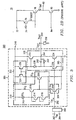
- Figure 3 is a circuit schematic diagram of an amplifier 200 having an output stage 201.
- Amplifier 200 may operate to source and sink an output current to a load 250 attached to output 244.
- Amplifier 200 also includes an input amplifier stage 260 which may comprise any one of a number of conventional input or gain stages that provide an appropriately large gain.
- An input voltage V in is coupled to input terminals 262 and 264 of input amplifier stage 260.
- Output stage 201 is coupled to the input amplifier 260 at input node 202.
- the output stage 201 is powered by a first power supply reference 246 and a second power supply reference 245. Although the second supply voltage reference 245 is shown as ground, it will be recognized that the output stage 201 could be powered via a split supply having positive and negative supply voltage references wherein the first power supply reference 246 remains +V BB and the second power supply reference 245 is designated, for example, -V BB .
- the output stage 201 includes a sink control circuit 204, a translinear loop circuit 210, a current mirror circuit 222 and an output driver 230.
- the output stage 201 includes an input node 202 for receiving an input voltage V in from input amplifier stage 260.
- the sink control circuit 204 includes current sinking sensor transistor 206 having a control region coupled to the input node 202, first current guiding regions coupled to ground, and a second current guiding region. As shown transistor 206 is a single NPN bipolar junction transistor. An input current I in through input node 202 drives transistor 206.
- Translinear loop circuit 210 is coupled in series between the csecond current guiding region of the current sinking sensor transistor 206 and the current mirror circuit 222.
- Translinear loop circuit 210 includes a current source 212, a first diode drop transistor 214, a second diode drop transistor 216, a first bias transistor 218, and a second bias transistor 220.
- Transistors 214, 216, 218 and 220 are NPN bipolar junction transistors.
- Current source 212 establishes the operating point and is coupled to the first power supply reference 246.
- the first diode drop transistor 214 first current guiding region and a directly coupled second current guiding region and control region.
- the current source 212 is coupled to the directly coupled second current guiding and control region of first diode drop transistor 214.
- Second diode drop transistor 216 having a second current guiding region coupled to ground and a directly coupled second current guiding and control regions is coupled in series with the first diode drop transistor 214.
- the second current guiding region of second npn diode drop transistor 216 is coupled to the first current guiding region of the first diode drop transistor 214.
- Current source 212 causes current flow I 1 in the two diode drop transistors 214 and 216.
- First bias transistor 218 has a second current guiding region coupled to first power supply reference 246, a control region coupled to output terminal of current source 212 and a first current guiding region coupled to the second current guiding region of current sinking sensor transistor 206.
- Second bias transistor 220 has a first current guiding region coupled to ground, a control region coupled to the first current guiding region of the first bias transistor 218 and a second current guiding region.
- V be-214 , V be-216 , V be-218 , and V be-220 represent the control region-first current guiding region voltages of transistors 214, 216, 218 and 220, respectively;
- a 214 , A 216 , A 218 and A 220 represent the first current guiding region area of each respective transistor; Is is the
- sinking current I 2 of the first bias transistor 218 is inversely proportional to boosting current I 3 of second bias transistor 220.
- Boosting current I 3 is proportional to the square of the current I 1 provided by current source 212. Accordingly, when the sinking current I 2 increases, the boosting current I 3 decreases.
- the current mirror circuit 222 is coupled in series between translinear loop circuit 210 and output driver 230.
- the current mirror circuit 222 has a first and second current mirror transistor, 224 and 226, respectively.
- Transistors 224 and 226 are PNP bipolar junction transistors.
- Current mirror circuit 222 provides a means of establishing the dc bias levels within the circuit within the accuracy of the matching or tracking properties of its monolithic components.
- the first current mirror transistor 224 has a first current guiding region coupled to the power supply reference 246 and directly coupled control and second current guiding regions.
- the second current guiding region of first current mirror transistor 224 is coupled to the second current guiding region of second bias transistor 220 in translinear loop circuit 210.
- the control region of the second current mirror transistor 226 is coupled to the control region of the first current mirror transistor 224.
- the first current guiding region of the second current mirror transistor 226 is coupled to the first power supply reference 246.
- the output driver includes a pair of diodes, 238 and 242, a sourcing and sinking circuitry, transistors 232 and 234, respectively, a current mirror transistor 236 and a resistor 240.
- Transistors 232, 234, and 236 are NPN bipolar junction transistors.
- the sourcing transistor 232 has a control region coupled to the second current guiding region of the second current mirror transistor 226, a second current guiding region coupled to the first power supply reference 246 and a first current guiding region.
- the sinking transistor 234 has a second current guiding region coupled to the first current guiding region of the sourcing transistor 232, a first current guiding region coupled to the second power supply reference 245 and a control region.
- the current mirror transistor 236 has a control region coupled to the control region of the sinking transistor 234 and the control region of the current sensor transistor 206, a first current guiding region coupled to the second power supply reference 245 and a second current guiding region.
- the diode 238 of output driver 230 is coupled in series between the second current guiding region of the current mirror transistor 226 and the second current guiding region of current mirror transistor 236.
- the resistor 240 is coupled between the diode 238 and the output node 244.
- Diode 242 is coupled in parallel to the resistor 240 to provide diode-resistor current limiting.
- amplifier 200 amplifies an input signal V in at input terminals 262 and 264 to produce an output signal V out for load 250 at node 244.
- the output signal V out of the output stage 201 is fed back into the negative terminal 264 of the input amplifier stage 260.
- An input signal V in is fed into the positive terminal 262 of the input amplifier stage 260.
- the operational amplifier 200 compares the output signal V out with the input signal V in , adjusting the output signal V out to match the magnitude of the input signal.
- the output stage 201 will compensate for the difference in voltage. The difference is eliminated using the sourcing and sinking circuitry 232 and 234 to source and sink current into the output node 244 raising and lowering the output voltage V out , respectively.
- the output stage 201 either sources current to load 250 or sinks current from load 250.
- the output of amplifier stage 201 is brought to a high potential voltage. This causes transistors 234 and 236 to conduct an insignificant amount of current. This is referred to as the "off" state of transistors 234 and 236.
- transistors 234 and 236 are coupled such that the control region current of 234 is mirrored or replicated in transistor 236.
- the current mirror circuit 222 provides a sufficient amount of current to drive sourcing transistor 232.
- the current in second current mirror transistor 226 increases when the current in sourcing transistor 232 decreases and visa versa.
- the boosting scheme prevents latch-up since (1) the boosting scheme depends on the amplifier's 200 input signal Vin and output signal Vout; and (2) the translinear loop 210 within the boosting scheme follows the amplifier's 200 main feedback.
- the current in sinking transistor 234 decreases, it signifies that the output stage 201 is sourcing current. Accordingly, the current in current sinking sensor 206 decreases. Since the sinking current I 2 is inversely proportional to boosting current I 3 , when the sinking current I 2 decreases (turning sinking transistor 234 "OFF"), boost current I 3 increases (turning sourcing transistor 232 "ON").
- the current mirror 222 mirrors the boosting current I 3 and, thus, provides more current to drive the sourcing transistor 232.
- Output stage 201 may also act as a current sink for load 250.
- the biasing provided by translinear loop 210 does not provide current boosting for the sinking capability of the amplifier 200. Accordingly, when the current in sinking transistor 234 increases, the current in current sinking sensor 206 increases, and consequently, the sinking current I 2 in first bias transistor 218 increases. During the sinking operation, the boosting current decreases and, thus, the sourcing transistor 232 turns "OFF" and the quiescent current in the output stage 200 is reduced.
- Current sinking sensor 206, sinking transistor 234 and current mirror transistor 236 are NPN bipolar junction transistors that have their control regions and first current guiding regions tied together to form a current mirror circuit; thus, the current in current sinking sensor transistor 206 and current mirror transistor 236 are equivalent to the current in sinking transistor 234.
- sinking current in sinking transistor 234 increases, the sinking current I 2 through bias transistor 218 increases which triggers the boosting current I 3 to decrease due to the fixed reference voltage across them.
- Resistor 240 provides this additional path for the current.
- the voltage potential across resistor 240 will increase until the diode 238 turns "ON”.
- the current through sourcing transistor 232 is controlled.
- the current through second current mirror transistor 226 flows through diode 238 and transistor 236; and thus, biases the sourcing transistor 232 and sinking transistor 234.
- This embodiment provides a power efficient bias solution with no burdensome positive feedback. Additionally, the disclosed embodiments have high positive power supply rejection ratio having no supply reference capacitors. Characteristics of amplifier 200 include operation at a low quiescent current and an output voltage within the range from approximately the value of a power supply voltage down to a ground potential.
- FIG 4 is an illustration in schematic form of an alternate output stage 300.
- the alternate output stage 300 is substantially identical to the output stage 201 illustrated in Figure 3, except that it provides a level shift transistor 350 to enhance the operating point of the output stage.
- the level shift transistor 350 has a first current guiding region coupled to ground and directly coupled control and second current guiding regions coupled to the first current guiding region of the first bias transistor 218 of the translinear loop circuit 210.
- the translinear loop circuit 210 operates on its own virtual ground which is the second current guiding region and control region of level shift transistor 350.
- the circuit of Figure 3 operates adequately without level shift transistor 350; yet, the current sinking sensor transistor 206 may be placed closer to saturation than desired.
- the voltage potential across current sinking sensor transistor 206 when the translinear loop circuit 210 is grounded is twice the amount of voltage drop from control region to first current guiding region, 2V be .
- the circuit begins sinking and sourcing strongly the control region to second current guiding region junction of current sinking sensor transistor 206 could become transiently forward biased.
- level shift transistor 350 enhances the operating point, raising voltage potential across current sinking sensor transistor 206 to three times the amount of voltage drop from control region to first current guiding region, 3V be .
- the design provides more bandwidth and less chance of saturation. If more second current guiding region to first current guiding region voltage V CE of current sinking sensor 206 is required, inserting at least one diode between second bias transistor 220 and level shift transistor 350 will supply more voltage across the transistor current sinking sensor 206 to keep the control region-second current guiding region junction reversed biased and; thus, supplying more gain.
- the disclosed exemplary embodiments to largely use bipolar transistors. Nonetheless, certain parts of the disclosed exemplary embodiments with the exclusion of the translinear loop 210 can be alternatively implemented with MOSFET devices.
Landscapes
- Engineering & Computer Science (AREA)
- Power Engineering (AREA)
- Physics & Mathematics (AREA)
- Nonlinear Science (AREA)
- Amplifiers (AREA)
Applications Claiming Priority (2)
| Application Number | Priority Date | Filing Date | Title |
|---|---|---|---|
| US11277898P | 1998-12-18 | 1998-12-18 | |
| US112778 | 1998-12-18 |
Publications (3)
| Publication Number | Publication Date |
|---|---|
| EP1014567A2 true EP1014567A2 (de) | 2000-06-28 |
| EP1014567A3 EP1014567A3 (de) | 2003-07-09 |
| EP1014567B1 EP1014567B1 (de) | 2009-10-14 |
Family
ID=22345797
Family Applications (1)
| Application Number | Title | Priority Date | Filing Date |
|---|---|---|---|
| EP99204415A Expired - Lifetime EP1014567B1 (de) | 1998-12-18 | 1999-12-20 | Verbesserungen an oder in Bezug auf einen Operationsverstärker |
Country Status (3)
| Country | Link |
|---|---|
| US (1) | US6292057B1 (de) |
| EP (1) | EP1014567B1 (de) |
| DE (1) | DE69941533D1 (de) |
Cited By (1)
| Publication number | Priority date | Publication date | Assignee | Title |
|---|---|---|---|---|
| CN115248341A (zh) * | 2022-04-08 | 2022-10-28 | 杰华特微电子股份有限公司 | 开关器件的电流检测电路及应用其的开关电源 |
Families Citing this family (8)
| Publication number | Priority date | Publication date | Assignee | Title |
|---|---|---|---|---|
| US6417733B1 (en) * | 1999-07-06 | 2002-07-09 | Texas Instruments Incorporated | High output voltage swing class AB operational amplifier output stage |
| US6930551B2 (en) * | 2003-08-08 | 2005-08-16 | Texas Instruments Incorporated | Zero voltage class AB minimal delay output stage and method |
| DE102004019584B4 (de) * | 2004-04-19 | 2007-03-15 | Detewe Systems Gmbh | Verfahren zum Betreiben einer Telekommunikationsverbindung zwischen zwei Telekommunikationsgeräten |
| US7053699B2 (en) * | 2004-05-11 | 2006-05-30 | Elantec Semiconductor, Inc. | Current output stages |
| US7777569B2 (en) * | 2009-01-21 | 2010-08-17 | Texas Instruments Incorporated | Anti-pop method and apparatus for class AB amplifiers |
| US7777574B1 (en) * | 2009-01-23 | 2010-08-17 | Texas Instruments Incorporated | Closed loop ramp up for pop and click reduction in an amplifier |
| US10090792B2 (en) * | 2016-12-08 | 2018-10-02 | Ford Global Technologies, Llc | Self-balancing parallel power devices with a temperature compensated gate driver |
| US11070181B2 (en) * | 2018-11-20 | 2021-07-20 | Macronix International Co., Ltd. | Push-pull output driver and operational amplifier using same |
Family Cites Families (17)
| Publication number | Priority date | Publication date | Assignee | Title |
|---|---|---|---|---|
| US4403200A (en) * | 1981-08-24 | 1983-09-06 | Motorola, Inc. | Output stage for operational amplifier |
| JP2543872B2 (ja) * | 1986-08-13 | 1996-10-16 | 株式会社東芝 | 増幅回路 |
| US4933645A (en) | 1986-11-21 | 1990-06-12 | Takafumi Kasai | Amplifier having a constant-current bias circuit |
| SG30646G (en) * | 1988-12-10 | 1995-09-01 | Motorola Inc | Amplifier output stage |
| GB9313840D0 (en) | 1993-07-05 | 1993-08-25 | Philips Electronics Uk Ltd | Cascaded amplifier |
| US5442320A (en) | 1994-06-09 | 1995-08-15 | National Semiconductor Corporation | Mirror and bias circuit for class AB output stage with large swing and output drive |
| US5500625A (en) | 1994-12-01 | 1996-03-19 | Texas Instruments Incorporated | Controlled current output stage amplifier circuit and method |
| US5491437A (en) | 1994-12-01 | 1996-02-13 | Texas Instruments Incorporated | Amplifier circuit and method |
| US5646576A (en) | 1995-07-24 | 1997-07-08 | Motorola | Output stage of operational amplifier suitable for mounting on a substrate and method of amplifying therewith |
| US5684432A (en) * | 1995-12-26 | 1997-11-04 | Lucent Technologies Inc. | Amplifier output stage having enhanced drive capability |
| US5798673A (en) | 1996-03-19 | 1998-08-25 | Motorola, Inc. | Low voltage operational amplifier bias circuit and method |
| JP3338280B2 (ja) * | 1996-03-19 | 2002-10-28 | 東芝デジタルメディアエンジニアリング株式会社 | 増幅器及び半導体装置 |
| US5699015A (en) | 1996-03-19 | 1997-12-16 | Motorola, Inc. | Low voltage operational amplifier and method |
| DE69628911D1 (de) * | 1996-04-26 | 2003-08-07 | St Microelectronics Srl | Leistungsstufe für einen Operationsverstärker |
| DE19634052C2 (de) * | 1996-08-23 | 1998-07-30 | Telefunken Microelectron | Verfahren zur Steuerung einer Gegentakt-Endstufe |
| US5963093A (en) * | 1997-02-04 | 1999-10-05 | Texas Instruments Incorporated | Class AB output stage wih reduced distortion |
| JP3120763B2 (ja) * | 1997-11-12 | 2000-12-25 | 日本電気株式会社 | 差動増幅器 |
-
1999
- 1999-12-13 US US09/459,949 patent/US6292057B1/en not_active Expired - Lifetime
- 1999-12-20 DE DE69941533T patent/DE69941533D1/de not_active Expired - Lifetime
- 1999-12-20 EP EP99204415A patent/EP1014567B1/de not_active Expired - Lifetime
Cited By (1)
| Publication number | Priority date | Publication date | Assignee | Title |
|---|---|---|---|---|
| CN115248341A (zh) * | 2022-04-08 | 2022-10-28 | 杰华特微电子股份有限公司 | 开关器件的电流检测电路及应用其的开关电源 |
Also Published As
| Publication number | Publication date |
|---|---|
| DE69941533D1 (de) | 2009-11-26 |
| EP1014567A3 (de) | 2003-07-09 |
| US6292057B1 (en) | 2001-09-18 |
| EP1014567B1 (de) | 2009-10-14 |
Similar Documents
| Publication | Publication Date | Title |
|---|---|---|
| US4570128A (en) | Class AB output circuit with large swing | |
| US5760652A (en) | Integrated circuit device | |
| US5212456A (en) | Wide-dynamic-range amplifier with a charge-pump load and energizing circuit | |
| US4480230A (en) | Large swing CMOS power amplifier | |
| US20040046532A1 (en) | Low dropout voltage regulator using a depletion pass transistor | |
| EP0476365A1 (de) | Adaptive Vorspannungsstromsteuerungsschaltung | |
| KR20030078630A (ko) | 요구응답 전원 부스트를 구비한 증폭기 시스템 | |
| US6891433B2 (en) | Low voltage high gain amplifier circuits | |
| KR0135971B1 (ko) | 회로 입력 신호의 차동 증폭용 전자 회로 | |
| US7262662B2 (en) | Operational amplifier | |
| JPH02162812A (ja) | 相補形カレント・ミラー回路を用いたダイアモンド・フォロワ回路及びゼロ・オフセットの増幅器 | |
| EP1014567B1 (de) | Verbesserungen an oder in Bezug auf einen Operationsverstärker | |
| US7459976B2 (en) | Apparatus and method for biasing cascode devices in a differential pair using the input, output, or other nodes in the circuit | |
| US4336503A (en) | Driver circuit having reduced cross-over distortion | |
| US6583669B1 (en) | Apparatus and method for a compact class AB turn-around stage with low noise, low offset, and low power consumption | |
| US20200007099A1 (en) | Amplifier class ab output stage | |
| US6614280B1 (en) | Voltage buffer for large gate loads with rail-to-rail operation and preferable use in LDO's | |
| JPH07263976A (ja) | バイアス補償及び緩衝手法を有するhbtモノリシック可変利得増幅回路 | |
| US6366169B1 (en) | Fast rail-to-rail class AB output stage having stable output bias current and linear performance | |
| US5880637A (en) | Low-power operational amplifier having fast setting time and high voltage gain suitable for use in sampled data systems | |
| US6741133B2 (en) | High output amplifier for stable operation | |
| US10566933B2 (en) | Low voltage amplifier with gain boost circuit | |
| US6417733B1 (en) | High output voltage swing class AB operational amplifier output stage | |
| US20030076163A1 (en) | Differential amplifying method and apparatus capable of responding to a wide input voltage range | |
| US5570064A (en) | Automatic gain control amplifier for use in radio transmitter-receiver |
Legal Events
| Date | Code | Title | Description |
|---|---|---|---|
| PUAI | Public reference made under article 153(3) epc to a published international application that has entered the european phase |
Free format text: ORIGINAL CODE: 0009012 |
|
| AK | Designated contracting states |
Kind code of ref document: A2 Designated state(s): AT BE CH CY DE DK ES FI FR GB GR IE IT LI LU MC NL PT SE |
|
| AX | Request for extension of the european patent |
Free format text: AL;LT;LV;MK;RO;SI |
|
| PUAL | Search report despatched |
Free format text: ORIGINAL CODE: 0009013 |
|
| AK | Designated contracting states |
Designated state(s): AT BE CH CY DE DK ES FI FR GB GR IE IT LI LU MC NL PT SE |
|
| AX | Request for extension of the european patent |
Extension state: AL LT LV MK RO SI |
|
| 17P | Request for examination filed |
Effective date: 20040109 |
|
| 17Q | First examination report despatched |
Effective date: 20040206 |
|
| AKX | Designation fees paid |
Designated state(s): DE FR GB |
|
| 17Q | First examination report despatched |
Effective date: 20040206 |
|
| GRAP | Despatch of communication of intention to grant a patent |
Free format text: ORIGINAL CODE: EPIDOSNIGR1 |
|
| GRAC | Information related to communication of intention to grant a patent modified |
Free format text: ORIGINAL CODE: EPIDOSCIGR1 |
|
| GRAS | Grant fee paid |
Free format text: ORIGINAL CODE: EPIDOSNIGR3 |
|
| GRAA | (expected) grant |
Free format text: ORIGINAL CODE: 0009210 |
|
| AK | Designated contracting states |
Kind code of ref document: B1 Designated state(s): DE FR GB |
|
| REG | Reference to a national code |
Ref country code: GB Ref legal event code: FG4D |
|
| REF | Corresponds to: |
Ref document number: 69941533 Country of ref document: DE Date of ref document: 20091126 Kind code of ref document: P |
|
| PLBE | No opposition filed within time limit |
Free format text: ORIGINAL CODE: 0009261 |
|
| 26N | No opposition filed |
Effective date: 20100715 |
|
| PGFP | Annual fee paid to national office [announced via postgrant information from national office to epo] |
Ref country code: GB Payment date: 20141124 Year of fee payment: 16 |
|
| PGFP | Annual fee paid to national office [announced via postgrant information from national office to epo] |
Ref country code: FR Payment date: 20141124 Year of fee payment: 16 |
|
| PGFP | Annual fee paid to national office [announced via postgrant information from national office to epo] |
Ref country code: DE Payment date: 20141222 Year of fee payment: 16 |
|
| REG | Reference to a national code |
Ref country code: DE Ref legal event code: R119 Ref document number: 69941533 Country of ref document: DE |
|
| GBPC | Gb: european patent ceased through non-payment of renewal fee |
Effective date: 20151220 |
|
| REG | Reference to a national code |
Ref country code: FR Ref legal event code: ST Effective date: 20160831 |
|
| PG25 | Lapsed in a contracting state [announced via postgrant information from national office to epo] |
Ref country code: GB Free format text: LAPSE BECAUSE OF NON-PAYMENT OF DUE FEES Effective date: 20151220 Ref country code: DE Free format text: LAPSE BECAUSE OF NON-PAYMENT OF DUE FEES Effective date: 20160701 |
|
| PG25 | Lapsed in a contracting state [announced via postgrant information from national office to epo] |
Ref country code: FR Free format text: LAPSE BECAUSE OF NON-PAYMENT OF DUE FEES Effective date: 20151231 |