EP1014705A2 - Dispositif de prise de vue - Google Patents
Dispositif de prise de vue Download PDFInfo
- Publication number
- EP1014705A2 EP1014705A2 EP99309413A EP99309413A EP1014705A2 EP 1014705 A2 EP1014705 A2 EP 1014705A2 EP 99309413 A EP99309413 A EP 99309413A EP 99309413 A EP99309413 A EP 99309413A EP 1014705 A2 EP1014705 A2 EP 1014705A2
- Authority
- EP
- European Patent Office
- Prior art keywords
- image
- inversion
- inverted
- photographing apparatus
- optical lens
- Prior art date
- Legal status (The legal status is an assumption and is not a legal conclusion. Google has not performed a legal analysis and makes no representation as to the accuracy of the status listed.)
- Withdrawn
Links
Images



Classifications
-
- H—ELECTRICITY
- H04—ELECTRIC COMMUNICATION TECHNIQUE
- H04N—PICTORIAL COMMUNICATION, e.g. TELEVISION
- H04N5/00—Details of television systems
- H04N5/222—Studio circuitry; Studio devices; Studio equipment
- H04N5/262—Studio circuits, e.g. for mixing, switching-over, change of character of image, other special effects ; Cameras specially adapted for the electronic generation of special effects
- H04N5/2628—Alteration of picture size, shape, position or orientation, e.g. zooming, rotation, rolling, perspective, translation
-
- H—ELECTRICITY
- H04—ELECTRIC COMMUNICATION TECHNIQUE
- H04N—PICTORIAL COMMUNICATION, e.g. TELEVISION
- H04N23/00—Cameras or camera modules comprising electronic image sensors; Control thereof
- H04N23/10—Cameras or camera modules comprising electronic image sensors; Control thereof for generating image signals from different wavelengths
Definitions
- the present invention relates to an image photographing apparatus for converting an image obtained through an optical lens into an electric signal and outputting it.
- a camera apparatus using a CCD Charge Coupled Device
- an image photographed through an optical lens is imaged on the CCD and is converted into an electric signal, and it is outputted at timing corresponding to a TV system.
- this camera apparatus according to design of an optical system of the lens, there is also a case in which up-and-down and right-and-left relation in imaging is inverted.
- a lens for a video camera is designed so that such a case does not occur.
- Japanese Patent Laid-Open No.78909/1994 discloses an image processing technique for inverting right-and-left relation of a radiation image of a human body obtained through X ray.
- Japanese Patent Laid-Open No.191185/1998 discloses a technique and a camera using a line memory to obtain a mirror image signal in which right-and-left relation is inverted.
- both of the publications do not disclose an image processing technique for inverting up-and-down and right-and-left relation of an image.
- Fig. 1 is a schematic view for explaining a conventional image photographing apparatus.
- an image captured through a lens 1 is projected onto a screen SC of an optical conversion adapter ADP, and is sent to CCDs 2R, 2G, and 2B of a video camera main body 10 in a state inverted in up-and-down and right-and-left relation through a conversion lens CL.
- an image photographing apparatus like this has such a large-scale structure that an image photographed through a lens is once imaged on a screen in a conversion adapter, and it is again inverted through a conversion lens, so that the apparatus becomes difficult to use in view of its size and weight. Besides, since the conversion lens is interposed, there also occurs a problem of deterioration in resolution.
- the image photographing apparatus of the invention comprises an optical lens for converging an image of an object to be captured, a photoelectric conversion portion for receiving the image converged through the optical lens and for converting it into an electric signal, and an image processing portion for electrically performing, on the basis of an inversion/non-inversion control signal, an inversion/non-inversion processing of positional relation which is in the electric signal obtained through conversion at the photoelectric conversion portion and which is at a time when the image was received.
- the image captured through the optical lens is converted into the electric signal at the photoelectric conversion portion, and the positional relation which is in the electric signal obtained through conversion at the photoelectric conversion portion and which is at the time when the image was captured is subjected to the inversion/non-inversion processing at the image processing portion. That is, in the case where an inversion signal is inputted to the image processing portion, the positional relation in the electric signal at the time of capture of the image, which was obtained through conversion at the photoelectric conversion portion, is inverted, and in the case where a non-inversion signal is inputted, the electric signal obtained through conversion at the photoelectric conversion portion is outputted as it is. By this, it becomes possible to electrically perform the inversion/non-inversion of an image according to the kind of the optical lens.
- Fig. 1 is a schematic view for explaining a conventional image photographing apparatus.
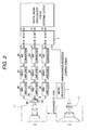
- Fig. 2 is a block diagram for explaining a structure of an image photographing apparatus of an embodiment of the invention.
- Fig. 3 is a block diagram of a main portion for explaining a signal processing portion.
- Fig. 4 is a schematic view for explaining writing/reading positions in each memory.
- Fig. 5 is a block diagram for explaining an address control circuit.
- FIG. 2 is a block diagram for explaining a structure of an image photographing apparatus in an embodiment. That is, this image photographing apparatus has a structure mainly comprising an optical lens 1 for converging an image of a subject as an object to be captured, CCDs 2R, 2G, and 2B for receiving the image converged by this optical lens 1 and for converting it into an electric signal, and an image processing portion 3 for performing an inversion/non-inversion processing of the image.
- an optical lens 1 for converging an image of a subject as an object to be captured
- CCDs 2R, 2G, and 2B for receiving the image converged by this optical lens 1 and for converting it into an electric signal
- an image processing portion 3 for performing an inversion/non-inversion processing of the image.
- this apparatus comprises a prism P for branching and dispersing the image captured through the optical lens 1 in three directions, a CCD 2R for converting a red component among the respective images branched and dispersed in the three directions into an electric signal, a CCD 2G for converting a green component into an electric signal, and a CCD 2B for converting a blue component into an electric signal.
- the electric signals outputted from the respective CCDs 2R, 2G, and 2B there are provided, for the respective output lines of the CCDs 2R, 2G, and 2B, preamplifiers 4R, 4G, and 4B, video amplifiers 5R, 5G, and 5B, and A/D converters 6R, 6G, and 6B, and the electric signals after processing are inputted to the image processing portion 3.
- the image processing portion 3 On the basis of an inversion/non-inversion signal outputted from a microprocessor 7, the image processing portion 3 performs an inversion/non-inversion processing of positional relation (for example, up-and-down and right-and-left relation) which is in the electric signal outputted from each of the CCDs 2R, 2G, and 2B and subjected to a predetermined processing and which is at the time when the image was received.
- positional relation for example, up-and-down and right-and-left relation
- the flow of image capturing will be described. That is, the image photographed through the optical lens 1 is separated into the three primary colors of R (red), G (green), and B (blue) by the prism P, each is imaged on the corresponding CCD 2R, 2G, or 2B in an inverted state, and is converted into an electric signal (analog).
- the electric signals outputted from the respective CCDs 2R, 2G, and 2B are converted into digital signals by the corresponding preamplifiers 4R, 4G, and 4B, the video amplifiers 5R, 5G, and 5B, and the A/D converters 6R, 6G, and 6B.
- the invention is not limited to this.
- a non-inversion control signal is inputted to the image processing portion 3 from the microprocessor 7.
- the digital signals outputted from the A/D converters 6R, 6G, and 6B and inputted to Rin, Gin, and Bin of the image processing portion 3 are outputted from Rout, Gout, and Bout as they are. That is, the inversion processing is not performed, but they are outputted in just the positional relation at the time of capture in the CCDs 2R, 2G, and 2B.
- an inversion control signal is inputted from the microprocessor 7 to the image processing portion 3.
- the digital signals outputted from the A/D converters 6R, 6G, and 6B and inputted to the Rin, Gin, and Bin of the image processing portion 3 are respectively outputted from the Rout, Gout, and Bout in the state where the positional relation (up-and-down and right-and-left relation) at the time when the image was received at the CCDs 2R, 2G, and 2B is inverted. That is, it becomes possible to electrically correct the up-and-down and right-and-left relation in imaging by the film lens 1'.
- Fig. 3 is a block diagram of a main portion for explaining the signal processing portion.
- the signal processing portion 3 includes bus lines corresponding to the three signals of R (red), G (green), and B (blue), and is constituted of, correspondingly to the respective bus lines, flip-flops FFR, FFG, and FFB, pairs of memories M1R and M2R, M1G and M2G, and M1B and M2B, and latches LTR, LTG, and LTB.
- the signals having passed through the respective flip-flops FFR, FFG, and FFB for R (red), G (green), and B (blue) are sent to the bus lines to which the memories M1R, M2R, M1G, M2G, M1B, and M2B are connected.
- the memories M1R, M2R, M1G, M2G, M1B, and M2B are in a standby state, the outputs of the memories M1R, M2R, M1G, M2G, M1B, and M2B are in a high impedance state.
- the input signals are applied to the respective latches LTR, LTG, and LTB as they are, and they are latched and are outputted.
- the signals having passed through the respective flip-flops FFR, FFG, and FFB for R (red), G (green), and B (blue) are written in one of the two memories M1R and M2R connected to the one bus line, one of the memories M1G and M2G, and one of the memories M1B and M2B.
- the other memories M2R or M1R, M2G or M1G, and M2B or M1B perform reading of the inverted signal.
- Writing/reading of the two memories is alternately changed for every field of a TV system. Since the bus line is common, writing/reading of the signal flows in time-sharing. For example, a piece of data for writing into one of the memories M1R and M2R, M1G and M2G, or M1B and M2B is outputted from the flip-flop FFR, FFG, or FFB, and immediately after the one of the memories M1R and M2R, M1G and M2G, or M1B and M2B captures it, the flip-flop FFR, FFG, or FFB comes to have a high impedance, the other memory M2R or M1R, M2G or M1G, or M2B or M1B outputs the read data to the bus line, and the latch LTR, LTG, or LTB latches and outputs it to the subsequent processing.
- Fig. 4 is a schematic view for explaining a writing/reading position in each memory.
- a head address of reading and writing is different according to a TV system (PAL or NTSC) to be handled.
- PAL or NTSC TV system
- FIG. 5 is a block diagram for explaining an address control circuit.
- This address control circuit comprises a counter CV for addresses (ROW addresses) in the vertical (V) direction in a memory, a counter CH for addresses (COLUMN addresses) in the horizontal (H) direction, a multiplexer MP for switching the ROW address/COLUMN address, and an EXOR (exclusive OR) circuit 8 for performing signal inversion for every field.
- the number of the provided EXOR circuits 8 is equal to the number (in this example, ten) corresponding to the number of output bits from the multiplexer MP, and each takes exclusive OR between a bit signal outputted from the multiplexer MP and a signal (FLD) indicating a field.
- FLD signal
- the value of an address is inverted/non-inverted for every field. That is, since the counters CV and CH produce addresses in ascending order, when their values are inverted by the EXOR circuits 8, the addresses are outputted in descending order, and when their values are non-inverted, the addresses are outputted in ascending order.
- an initial value corresponding to the address (see the arrows 1 ⁇ and 2 ⁇ in Fig. 4) of the writing/reading start position of a signal corresponding to a TV system (PAL or NTSC) is given to the counter CV in the vertical direction and the counter CH in the horizontal direction.
- Such inversion/non-inversion of the signal is designed to be switched in the case where the optical lens is exchanged as described before.
- a lens for a large film has a shallow depth of field as compared with a normal lens for a video camera, it is possible to take such a picture that the background of a subject to be photographed is blurred, and only the subject is brought into focus and is accented.
- the image photographing apparatus of the present invention the following effects are obtained. That is, in the case where it is desired to exchange an optical lens, the positional relation of a captured image can be electrically inverted without using an optical converting adapter, so that it becomes possible to use various lenses without increasing the size and weight of the image photographing apparatus. Besides, since a converting adapter is not used, it becomes possible to prevent deterioration of picture quality in the case of exchange of lenses.
Landscapes
- Engineering & Computer Science (AREA)
- Multimedia (AREA)
- Signal Processing (AREA)
- Studio Circuits (AREA)
- Transforming Light Signals Into Electric Signals (AREA)
- Studio Devices (AREA)
- Color Television Image Signal Generators (AREA)
- Image Processing (AREA)
Applications Claiming Priority (2)
| Application Number | Priority Date | Filing Date | Title |
|---|---|---|---|
| JP35708598A JP3307350B2 (ja) | 1998-12-16 | 1998-12-16 | 画像処理装置 |
| JP35708598 | 1998-12-16 |
Publications (2)
| Publication Number | Publication Date |
|---|---|
| EP1014705A2 true EP1014705A2 (fr) | 2000-06-28 |
| EP1014705A3 EP1014705A3 (fr) | 2002-01-30 |
Family
ID=18452315
Family Applications (1)
| Application Number | Title | Priority Date | Filing Date |
|---|---|---|---|
| EP99309413A Withdrawn EP1014705A3 (fr) | 1998-12-16 | 1999-11-25 | Dispositif de prise de vue |
Country Status (3)
| Country | Link |
|---|---|
| US (1) | US6697115B1 (fr) |
| EP (1) | EP1014705A3 (fr) |
| JP (1) | JP3307350B2 (fr) |
Cited By (2)
| Publication number | Priority date | Publication date | Assignee | Title |
|---|---|---|---|---|
| EP1237362A1 (fr) * | 2001-02-28 | 2002-09-04 | Benjamin Gabel | Caméra vidéo et adaptateur pour caméra vidéo |
| EP1699229A1 (fr) * | 2005-03-02 | 2006-09-06 | Thomson Licensing | Méthode, circuiterie et caméra pour l'inversion electronique du balayage |
Families Citing this family (1)
| Publication number | Priority date | Publication date | Assignee | Title |
|---|---|---|---|---|
| JP2002247593A (ja) * | 2001-02-16 | 2002-08-30 | Olympus Optical Co Ltd | 画像処理装置 |
Family Cites Families (8)
| Publication number | Priority date | Publication date | Assignee | Title |
|---|---|---|---|---|
| JPH0827604B2 (ja) * | 1986-06-18 | 1996-03-21 | 株式会社日立製作所 | 画像表示システム |
| JPH03282497A (ja) * | 1990-03-30 | 1991-12-12 | Toshiba Corp | 信号変換方式および装置 |
| EP0456414A3 (en) * | 1990-05-11 | 1992-05-20 | Matsushita Electric Industrial Co., Ltd | Slant correction for a video camera apparatus |
| US5270831A (en) * | 1990-09-14 | 1993-12-14 | Eastman Kodak Company | Storage and playback of digitized images in digital database together with presentation control file to define image orientation/aspect ratio |
| JP3050474B2 (ja) * | 1993-12-01 | 2000-06-12 | シャープ株式会社 | モニタ画面一体型ビデオカメラ |
| JPH0895551A (ja) * | 1994-09-28 | 1996-04-12 | Nikon Corp | 画像表示装置 |
| US6011585A (en) * | 1996-01-19 | 2000-01-04 | Apple Computer, Inc. | Apparatus and method for rotating the display orientation of a captured image |
| US6262769B1 (en) * | 1997-07-31 | 2001-07-17 | Flashpoint Technology, Inc. | Method and system for auto rotating a graphical user interface for managing portrait and landscape images in an image capture unit |
-
1998
- 1998-12-16 JP JP35708598A patent/JP3307350B2/ja not_active Expired - Fee Related
-
1999
- 1999-11-25 EP EP99309413A patent/EP1014705A3/fr not_active Withdrawn
- 1999-12-14 US US09/460,542 patent/US6697115B1/en not_active Expired - Fee Related
Cited By (6)
| Publication number | Priority date | Publication date | Assignee | Title |
|---|---|---|---|---|
| EP1237362A1 (fr) * | 2001-02-28 | 2002-09-04 | Benjamin Gabel | Caméra vidéo et adaptateur pour caméra vidéo |
| WO2002069622A1 (fr) * | 2001-02-28 | 2002-09-06 | P+S Technik Gmbh | Videocamera et adaptateur de videocamera |
| US7092025B2 (en) | 2001-02-28 | 2006-08-15 | P & S Technik | Video camera adapter for providing decreased depth of focus |
| US7719599B2 (en) | 2001-02-28 | 2010-05-18 | P&S Technik Gmbh | Adapter for video camera for providing decreased depth of focus |
| EP1699229A1 (fr) * | 2005-03-02 | 2006-09-06 | Thomson Licensing | Méthode, circuiterie et caméra pour l'inversion electronique du balayage |
| US7855736B2 (en) | 2005-03-02 | 2010-12-21 | Thomson Licensing | Method, circuit arrangement and camera for providing electronic scan reversal |
Also Published As
| Publication number | Publication date |
|---|---|
| JP3307350B2 (ja) | 2002-07-24 |
| EP1014705A3 (fr) | 2002-01-30 |
| US6697115B1 (en) | 2004-02-24 |
| JP2000184296A (ja) | 2000-06-30 |
Similar Documents
| Publication | Publication Date | Title |
|---|---|---|
| US4951135A (en) | Electronic-type endoscope system having capability of setting AGC variation region | |
| US4831453A (en) | Solid-state imaging device having high-speed shutter function and method of realizing high-speed function in solid-state imaging device | |
| US5694165A (en) | High definition image taking apparatus having plural image sensors | |
| US20020158973A1 (en) | Image-taking apparatus and image-taking method | |
| JPH10210367A (ja) | 電子的撮像装置 | |
| JPH1118097A (ja) | 撮像装置及び撮像方法及びその撮像方法を記録した記録媒体 | |
| US7236194B2 (en) | Image signal processing apparatus | |
| JPH06133321A (ja) | Ccd撮像装置 | |
| US6697115B1 (en) | Image photographing apparatus for electrically performing inversion/non-inversion of captured pictures | |
| US7230646B2 (en) | Single sensor electronic video camera technique with diagonally coupled pixels | |
| EP0441345A1 (fr) | Caméra pour les images fixes de haute définition | |
| KR970002141B1 (ko) | 고체컬러촬상장치 | |
| JP3346481B2 (ja) | 動画入力装置 | |
| JP3397397B2 (ja) | 撮像装置 | |
| JPS62190980A (ja) | 高解像度テレビジヨンカメラ | |
| JPH09224180A (ja) | 撮像装置 | |
| JP2713295B2 (ja) | 固体撮像素子の駆動方法と撮像装置 | |
| JP2000244821A (ja) | 撮像装置 | |
| RU98102201A (ru) | Способ получения телевизионного изображения высокой четкости в камере на обычных пзс и устройство для реализации этого способа | |
| JPH01138875A (ja) | カラーテレビカメラ | |
| JPS63123286A (ja) | 電子スチルカメラ | |
| JPH06350904A (ja) | カメラ | |
| JPH08307776A (ja) | 撮像装置 | |
| JPH05276452A (ja) | 撮像装置 | |
| JP2004112723A (ja) | 撮像素子及び撮像装置 |
Legal Events
| Date | Code | Title | Description |
|---|---|---|---|
| PUAI | Public reference made under article 153(3) epc to a published international application that has entered the european phase |
Free format text: ORIGINAL CODE: 0009012 |
|
| AK | Designated contracting states |
Kind code of ref document: A2 Designated state(s): AT BE CH CY DE DK ES FI FR GB GR IE IT LI LU MC NL PT SE Kind code of ref document: A2 Designated state(s): DE FR GB |
|
| AX | Request for extension of the european patent |
Free format text: AL;LT;LV;MK;RO;SI |
|
| PUAL | Search report despatched |
Free format text: ORIGINAL CODE: 0009013 |
|
| AK | Designated contracting states |
Kind code of ref document: A3 Designated state(s): AT BE CH CY DE DK ES FI FR GB GR IE IT LI LU MC NL PT SE |
|
| AX | Request for extension of the european patent |
Free format text: AL;LT;LV;MK;RO;SI |
|
| 17P | Request for examination filed |
Effective date: 20020711 |
|
| AKX | Designation fees paid |
Free format text: DE FR GB |
|
| STAA | Information on the status of an ep patent application or granted ep patent |
Free format text: STATUS: THE APPLICATION IS DEEMED TO BE WITHDRAWN |
|
| 18D | Application deemed to be withdrawn |
Effective date: 20060601 |