EP1016140B1 - Procede de cablage pour composants a semi-conducteur destines a empecher le piratage et la manipulation des produits, composant a semi-conducteur produit selon ce procede et utilisation du composant a semi-conducteur dans une carte a puce - Google Patents
Procede de cablage pour composants a semi-conducteur destines a empecher le piratage et la manipulation des produits, composant a semi-conducteur produit selon ce procede et utilisation du composant a semi-conducteur dans une carte a puce Download PDFInfo
- Publication number
- EP1016140B1 EP1016140B1 EP98951273A EP98951273A EP1016140B1 EP 1016140 B1 EP1016140 B1 EP 1016140B1 EP 98951273 A EP98951273 A EP 98951273A EP 98951273 A EP98951273 A EP 98951273A EP 1016140 B1 EP1016140 B1 EP 1016140B1
- Authority
- EP
- European Patent Office
- Prior art keywords
- substrate
- component
- semiconductor component
- layer
- conducting
- Prior art date
- Legal status (The legal status is an assumption and is not a legal conclusion. Google has not performed a legal analysis and makes no representation as to the accuracy of the status listed.)
- Expired - Lifetime
Links
Images


Classifications
-
- H—ELECTRICITY
- H10—SEMICONDUCTOR DEVICES; ELECTRIC SOLID-STATE DEVICES NOT OTHERWISE PROVIDED FOR
- H10W—GENERIC PACKAGES, INTERCONNECTIONS, CONNECTORS OR OTHER CONSTRUCTIONAL DETAILS OF DEVICES COVERED BY CLASS H10
- H10W20/00—Interconnections in chips, wafers or substrates
- H10W20/01—Manufacture or treatment
- H10W20/021—Manufacture or treatment of interconnections within wafers or substrates
- H10W20/023—Manufacture or treatment of interconnections within wafers or substrates the interconnections being through-semiconductor vias
-
- H—ELECTRICITY
- H10—SEMICONDUCTOR DEVICES; ELECTRIC SOLID-STATE DEVICES NOT OTHERWISE PROVIDED FOR
- H10D—INORGANIC ELECTRIC SEMICONDUCTOR DEVICES
- H10D89/00—Aspects of integrated devices not covered by groups H10D84/00 - H10D88/00
-
- H—ELECTRICITY
- H10—SEMICONDUCTOR DEVICES; ELECTRIC SOLID-STATE DEVICES NOT OTHERWISE PROVIDED FOR
- H10W—GENERIC PACKAGES, INTERCONNECTIONS, CONNECTORS OR OTHER CONSTRUCTIONAL DETAILS OF DEVICES COVERED BY CLASS H10
- H10W42/00—Arrangements for protection of devices
- H10W42/20—Arrangements for protection of devices protecting against electromagnetic or particle radiation, e.g. light, X-rays, gamma-rays or electrons
-
- H—ELECTRICITY
- H10—SEMICONDUCTOR DEVICES; ELECTRIC SOLID-STATE DEVICES NOT OTHERWISE PROVIDED FOR
- H10W—GENERIC PACKAGES, INTERCONNECTIONS, CONNECTORS OR OTHER CONSTRUCTIONAL DETAILS OF DEVICES COVERED BY CLASS H10
- H10W42/00—Arrangements for protection of devices
- H10W42/40—Arrangements for protection of devices protecting against tampering, e.g. unauthorised inspection or reverse engineering
-
- Y—GENERAL TAGGING OF NEW TECHNOLOGICAL DEVELOPMENTS; GENERAL TAGGING OF CROSS-SECTIONAL TECHNOLOGIES SPANNING OVER SEVERAL SECTIONS OF THE IPC; TECHNICAL SUBJECTS COVERED BY FORMER USPC CROSS-REFERENCE ART COLLECTIONS [XRACs] AND DIGESTS
- Y10—TECHNICAL SUBJECTS COVERED BY FORMER USPC
- Y10S—TECHNICAL SUBJECTS COVERED BY FORMER USPC CROSS-REFERENCE ART COLLECTIONS [XRACs] AND DIGESTS
- Y10S438/00—Semiconductor device manufacturing: process
- Y10S438/977—Thinning or removal of substrate
Definitions
- the present invention relates to a method for producing one with one or more conductive structural elements provided semiconductor device with the features of the preamble of claim 1 and one provided with one or more conductive structural elements Semiconductor component that can be produced by such a method.
- a method for producing a metallized semiconductor circuit structure which is feasible with CMOS-compatible standard semiconductor technologies and the use of so-called reverse engineering to acquire foreign technology know-how or for reading out and / or for manipulating the information stored in the component difficult.
- the method according to the invention also makes it possible to compare one Manufacture environmental protected semiconductor device.
- a method with the features of the preamble of claim 1 is, for example, from G. Schumiki, P. Seegebrecht “Process Technology", Springer-Verlag Berlin, ISBN 3-540-17670-5 known.
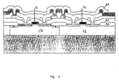
- 5 shows a semiconductor device produced by such a method.
- the passivation or insulator layers designated by reference numeral 11 the layers denoted by reference numeral 12 represent conductive layers, for example are made of doped semiconductor material or doped poly-silicon layers, and the Layers denoted by reference numeral 13 represent metallizations.
- the wiring 13 of the Component is made by means of deposition and structuring of metal layers and in between Insulator layers 11 realized. In this modular process, contact holes are created etched through an insulator layer 11 to a conductive structure 12, 13, then a metal layer deposited and subsequently structured conductor tracks 13 and again with an insulator layer 11 covered.
- semiconductor components can be optically irradiated, and their design can be easily "seen through” by means of electron beam microscopy, either using imaging methods or else by following a flowing current.
- semiconductor components can be optically irradiated, and their design can be easily "seen through” by means of electron beam microscopy, either using imaging methods or else by following a flowing current.
- it is also customary to remove mechanically or chemically layer by layer of a semiconductor component and then to examine the surface that results in each case.
- Chip card manipulation options for third parties are given to the security of chip cards severely affect. For example, it is possible through special techniques in the chip cards read stored information and change it if necessary.
- the component substrate now present is subsequently joined together with a handling substrate from the front to the front, and the component substrate can additionally be thinned from the rear.
- the subsequent provision of electrical contacts to the component i.e. the provision of the metallization level following the component layer within the substrate without metallization, with one or more metallization levels, is carried out by etching contact holes after a corresponding lithography step through the possibly thinned component substrate layer to the areas to be contacted and subsequently metallized.
- the sequence of the steps of the method according to the invention introduces an additional substrate into the component.
- This substrate can either be the component substrate itself or, in the case of an iterative repetition of the method steps according to claim 12, be the handling substrate which was introduced in the preceding iteration step and has accordingly assumed the role of the component substrate.
- the additional substrate can be arranged, for example, between the semiconductor component per se and the metallization level (s) provided for the electrical contacting of the semiconductor component.
- the additional substrate can also be arranged between individual metallization levels provided for the electrical contacting of the semiconductor component.
- the expression “metallization levels” here includes all conductive structural elements of the semiconductor component, for example conductor tracks, wiring, etc.
- the component substrate and the handling substrate are firmly connected to one another in such a way that there can then be no nondestructive separation of the layer stack.
- the substrate additionally introduced into the component is made of a material that is not transparent in the range of visible wavelengths, for example of silicon, so that the use of optical transmission methods is prevented.
- the additional substrate can additionally contain or be made of a material that is not transparent in the region of short-wave radiation, for example X-rays, so that the use of X-ray radiation methods is prevented.
- the additional substrate can also be a so-called SOI substrate, so that the buried insulator layer serves as an etching stop in an etching step. This can further simplify the manufacturing process and reduce its cost. Furthermore, when using an SOI substrate, it is possible to etch the additional substrate more uniformly.
- the The front side of the component substrate is preferably provided with an adhesive layer.
- the adhesive layer can take on a passivating and / or planarizing function at the same time.
- the component substrate is thinned from the back.
- the thinning can for example by wet chemical etching or by mechanical or chemomechanical Loops are done.
- the substrate stack present after the joining and thinning can then be processed as a standard substrate, with the surface of the thinned Component substrate now represents the front. This is done first by deposition a dielectric layer isolated, under certain circumstances when using an SOI substrate this insulation can be dispensed with.
- the substrate wafer can be reduced to the necessary thickness by the substrate stack from the handling substrate side is thinned mechanically and / or chemically.
- the possibilities of product piracy and product manipulation are advantageously countered compared to the methods for multilayer wiring known according to the current state of the art, since parts of the component wiring are shifted to the side of the component substrate which are part of the component itself or also other parts of the component Component wiring is opposite.
- structured metal layers arranged one above the other are insulated from one another by optically transparent dielectric layers, for example SiO 2 , as shown in FIG. 5.
- the additional substrate which, as explained above, the component substrate itself or even a handling substrate can be the complexity of the wiring can be increased, as a result of which the commonly used techniques for analyzing the circuit structure and techniques for manipulating the information stored in the components are prevented or become more difficult. If the additional substrate is also not optically transparent is a method for optical fluoroscopy or analysis using electron beam microscopy prevented, on the other hand, procedures for manipulation or reading out the information contained in the circuit or in the chip card is no longer applicable.
- the method according to the invention can be used to compare one Manufacture environmental protected semiconductor device.
- the first serves Substrate layer, which is now an intermediate layer within the semiconductor component, as a protective layer against environmental influences. By choosing a suitable material this protective function can be increased for the first substrate.
- protective layers can be applied before the step of providing the or one of the plurality of conductive structural elements in order to increase the protective function.
- protective layers can be passivation layers, for example made of SiO 2 .
- FIG. 1 shows a component substrate with completely processed MOS circuits and a metallization level before connecting to an auxiliary substrate.
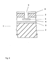
- FIG. 2 shows the component substrate shown in FIG. 1 after connection to the auxiliary substrate and Thinning the device substrate.
- FIG. 3 shows the disk stack shown in FIG. 2, which is processed like a standard disk.
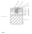
- FIG. 4 shows the disk stack shown in FIG. 3, which has now been provided with a wiring level on its surface.
- FIG. 5 shows a typical layer structure of a semiconductor component with a plurality of conductive structural elements, which is produced according to standard methods.
- reference numeral 1 denotes a component substrate, which comprises, for example, a silicon wafer 2 with finished MOS circuits and a metallization level 3.
- the metallization level 3 is passivated with an oxide protective layer.
- the metallization comprises, for example, an aluminum alloy.
- a polyimide layer 5 is spun onto the component wafer as an adhesive layer, so that the surface topography is leveled.
- the surface topography can also have been leveled by a planarization step before the adhesive layer is applied.
- the component wafer is then connected to an auxiliary substrate 6, for example a further silicon wafer.
- the stack of wafers now present is then thinned mechanically, post-chemically and / or chemomechanically from the side of the component substrate, so that the silicon remaining thickness of the component substrate is a few micrometers.
- the disk stack 7, which is shown for example in FIG. 2, can be like one Standard slice can be processed.
- the silicon surface is passivated, e.g. with an oxide layer 8.
- contact holes 9 are after a corresponding lithography step down to the areas to be contacted Metallization etched as shown in FIG. 3. Then, as shown in Fig. 4, are preferred the side walls of the contact holes are insulated with insulating layers 10. According to one particularly In a preferred embodiment, this is done by a so-called spacer oxide process sequence, conformal oxide deposition and subsequent anisotropic etching back includes.
- the circuits are wired, for example, by depositing a titanium nitride layer 11 as an adhesive and barrier layer for the subsequent tungsten metallization 12, which can be done, for example, by UV deposition.
- the tungsten / titanium nitride layer is then removed from the substrate surface using chemomechanical grinding with a CMP device, so that the remaining tungsten / titanium nitride "plugs" (so-called plugs) realize the vertical connection to the component metallization level.
- the wiring of the component is carried out by a standard metallization process, for example with an aluminum alloy 13 and subsequent passivation 14, as shown in FIG. 4.
- the wiring of the component can also comprise several metallization levels.
- the stack of discs is preferably mechanically from the auxiliary substrate side to the necessary residual thickness, for. B. 180 microns, thinned.
- the auxiliary substrate 6 and / or the component substrate 1 can be processed and / or structured in various ways after possibly thinning the component substrate.
- virtual interconnects that have no connections to the component can be produced in these substrates in order to deliberately supply incorrect information during reverse engineering. It is also possible to connect the planarized surface of the component processed according to FIG. 4 to a further auxiliary substrate in order to introduce a further auxiliary substrate layer into the resulting component.
- the multiple wiring levels comprises, these are separated from each other by an additional auxiliary substrate added.
- the semiconductor component produced by the method according to the invention can be particularly suitable use advantageously in chip cards, because of its special structure the manipulation possibilities are severely restricted from the outside. It is particularly difficult for counterfeiters, for example penetrate with metal pins through the individual component layers, thereby thereby the in read out and / or falsify information stored on the chip.
Landscapes
- Internal Circuitry In Semiconductor Integrated Circuit Devices (AREA)
- Semiconductor Integrated Circuits (AREA)
- Storage Device Security (AREA)
- Metal-Oxide And Bipolar Metal-Oxide Semiconductor Integrated Circuits (AREA)
Claims (20)
- Procédé pour fabriquer un composant semi-conducteur pourvu d'un ou de plusieurs éléments structurels conducteurs selon les étapes suivantes :application et structuration de couches (3, 4, 5) présentes dans le composant semi-conducteur, sur un premier substrat (1), caractérisé par les étapes suivantes :liaison tellement ferme de la surface supérieure du premier substrat (1) sur laquelle ces différentes couches sont appliquées, à un second substrat (6) qu'une séparation sans endommagement des deux substrats soit impossible,la mise à disposition du ou d'un des multiples éléments structurels (12, 13) conducteurs sur la surface supérieure libre du premier substrat ; cette étape étant réalisée de manière à créer directement un contact électrique fonctionnel à travers le premier substrat ( 1 ) entre l'élément structurel conducteur (13) et les couches (3, 4, 5), etréalisation du composant semi-conducteur.
- Procédé selon la revendication 1, caractérisé en ce que le premier substrat (1) n'est pas transparent dans les zones de longueurs d'ondes visibles.
- Procédé selon la revendication 1 ou 2, caractérisé en ce que le premier substrat (1) est un substrat Si.
- Procédé selon la revendication 1 ou 2, caractérisé en ce que le premier substrat (1) est un substrat SOI.
- Procédé selon une des revendications 1 à 4, caractérisé par l'étape où on rend mince le premier substrat (1) après l'étape de liaison de la surface supérieure du premier substrat (1) avec le second substrat (6).
- Procédé selon la revendication 5, caractérisé en ce que l'on rend mince par décapage, un ponçage mécanique ou chimico-mécanique ou une combinaison de ces procédés.
- Procédé selon une des revendications 1 à 6, caractérisé en ce que l'étape pour lier la surface supérieure du premier substrat (1) avec le second substrat (6), comprend l'étape d'application d'une couche (5) transmettant l'adhésion.
- Procédé selon la revendication 7, caractérisé en ce que la couche (5) transmettant l'adhésion est une couche polyamide.
- Procédé selon une des revendications 1 à 8, caractérisé en ce que l'étape pour lier la surface supérieure du premier substrat (1) au second substrat (6) est réalisée de manière à ce que la première couche de substrat (1) soit disposée dans le composant semi-conducteur entre le composant semi-conducteur lui-même et les plans de métallisation prévus pour le contact électrique du composant semi-conducteur.
- Procédé selon une des revendications 1 à 8, caractérisé en ce que l'étape pour relier la surface supérieure du premier substrat (1) avec le second substrat (6) est réalisée de manière à ce que la première couche de substrat (1) soit disposée dans le composant semi-conducteur entre différents plans de métallisation prévus pour le contact électrique du semi-conducteur.
- Procédé selon une des revendications 1 à 8, caractérisé en ce que l'étape pour relier la surface supérieure du premier substrat (1) avec le second substrat (6) est réalisé de manière à ce que la première couche de substrat (1) soit disposée dans le composant semi-conducteur entre les plans de métallisation prévus pour le contact électrique du composant semi-conducteur et un câblage prévu pour le contact électrique des plans de métallisation.
- Procédé selon une des revendications 1 à 8, caractérisé en ce que l'étape pour réaliser le composant semi-conducteur comprend une ou plusieurs étapes pour :relier la surface supérieure de la succession de couches mises à disposition avec un nième substrat (n > 2) ,etla mise à disposition d'un élément structurel conducteur supplémentaire sur la surface supérieure libre du substrat (n-1); cette étape étant réalisée de manière à ce qu'un contact électrique fonctionnel soit créée de façon directe à travers le substrat (n-1) entre l'élément structurel conducteur et le composant.
- Procédé selon une des revendications 1 à 8 et 12, caractérisé par l'étape pour structurer le premier ou le (n-1)ième substrat avant l'étape de mise à disposition du ou d'un des multiples éléments structurels sur la surface supérieure libre du premier ou du (n-1) substrat.
- Procédé selon une des revendications 1 à 8, 12 et 13, caractérisé par l'étape pour appliquer (en partie) une couche conductrice supplémentaire sur la surface supérieure libre du premier ou (n-1)ième substrat.
- Procédé selon la revendication 14, caractérisé par l'étape de liaison de la surface supérieure de substrat pourvue d'une couche conductrice supplémentaire avec un autre substrat.
- Procédé selon une des revendications 1 à 8, 12 et 13, caractérisé par plusieurs étapes se suivant destinées à appliquer (en partie) une couche conductrice supplémentaire sur la surface supérieure libre du premier ou (n-1)ième substrat et pour relier la surface supérieure du substrat pourvue d'une couche conductrice supplémentaire avec un autre substrat.
- Procédé selon une des revendications 1 à 16 pour fabriquer un composant semi-conducteur pourvu d'un ou de plusieurs éléments structurels conducteurs, lequel est protégé des influences de l'environnement.
- Procédé selon la revendication 17, caractérisé par l'étape d'application d'une ou de plusieurs couches de protection supplémentaires avant l'étape de mise à disposition du ou d'un des multiples éléments structurels conducteurs sur la surface supérieure libre du premier substrat.
- Avec un ou plusieurs composant semi-conducteur pourvu de multiples éléments structurels conducteurs, susceptibles d'être fabriqués par le procédé selon une des revendications 1 à 18, composé au moins d'un premier substrat (1) avec une première surface supérieure sur laquelle des couches (3, 4, 5) structurées sont appliquées en tant que couches de composants, et d'un second substrat (6) qui est relié avec la première surface supérieure du premier substrat ( 1) de manière tellement ferme qu'aucune séparation sans endommagement des deux substrats n'intervienne ; un ou plusieurs éléments structurels (12, 13) conducteurs se trouvant appliqués sur une surface supérieure libre du premier substrat et un contact électrique fonctionnel entre les éléments structurels (13) conducteurs et la couche des composants (3, 4, 5) étant ainsi créée.
- Utilisation du composant semi-conducteur selon la revendication 19 dans une carte à puce.
Applications Claiming Priority (5)
| Application Number | Priority Date | Filing Date | Title |
|---|---|---|---|
| DE19741507 | 1997-09-19 | ||
| DE19741507 | 1997-09-19 | ||
| DE19746641A DE19746641B4 (de) | 1997-09-19 | 1997-10-22 | Verdrahtungsverfahren für Halbleiter-Bauelemente zur Verhinderung von Produktpiraterie und Produktmanipulation und Verwendung des Halbleiter-Bauelements in einer Chipkarte |
| DE19746641 | 1997-10-22 | ||
| PCT/DE1998/002645 WO1999016131A1 (fr) | 1997-09-19 | 1998-09-04 | Procede de cablage pour composants a semi-conducteur destines a empecher le piratage et la manipulation des produits, composant a semi-conducteur produit selon ce procede et utilisation du composant a semi-conducteur dans une carte a puce |
Publications (2)
| Publication Number | Publication Date |
|---|---|
| EP1016140A1 EP1016140A1 (fr) | 2000-07-05 |
| EP1016140B1 true EP1016140B1 (fr) | 2003-11-19 |
Family
ID=26040160
Family Applications (1)
| Application Number | Title | Priority Date | Filing Date |
|---|---|---|---|
| EP98951273A Expired - Lifetime EP1016140B1 (fr) | 1997-09-19 | 1998-09-04 | Procede de cablage pour composants a semi-conducteur destines a empecher le piratage et la manipulation des produits, composant a semi-conducteur produit selon ce procede et utilisation du composant a semi-conducteur dans une carte a puce |
Country Status (5)
| Country | Link |
|---|---|
| US (1) | US6284627B1 (fr) |
| EP (1) | EP1016140B1 (fr) |
| JP (1) | JP2001517874A (fr) |
| AT (1) | ATE254803T1 (fr) |
| WO (1) | WO1999016131A1 (fr) |
Families Citing this family (8)
| Publication number | Priority date | Publication date | Assignee | Title |
|---|---|---|---|---|
| DE10043955A1 (de) * | 2000-09-06 | 2002-04-04 | Infineon Technologies Ag | Halbleiterchip mit einer Schutzabdeckung und zugehöriges Herstellungsverfahren |
| DE10058078C1 (de) * | 2000-11-23 | 2002-04-11 | Infineon Technologies Ag | Integrierte Schaltungsanordnung mit Analysierschutz und Verfahren zur Herstellung der Anordnung |
| DE10105725B4 (de) * | 2001-02-08 | 2008-11-13 | Infineon Technologies Ag | Halbleiterchip mit einem Substrat, einer integrierten Schaltung und einer Abschirmvorrichtung |
| JP4071615B2 (ja) * | 2002-12-20 | 2008-04-02 | 株式会社フジクラ | 貫通電極の形成方法及び貫通電極付き基板 |
| DE10323394B4 (de) * | 2003-05-20 | 2006-09-28 | Fraunhofer-Gesellschaft zur Förderung der angewandten Forschung e.V. | Verfahren zum Erzeugen einer elektrischen Kontaktierung zwischen zwei Halbleiterstücken und Verfahren zum Herstellen einer Anordnung von Halbleiterstücken |
| DE102004056970B4 (de) * | 2004-11-25 | 2008-07-03 | Fraunhofer-Gesellschaft zur Förderung der angewandten Forschung e.V. | Verfahren und Vorrichtung zum Erzeugen einer elektrischen Kontaktierung zwischen zwei Halbleiterstücken durch ein mechanisches Element |
| US7994042B2 (en) * | 2007-10-26 | 2011-08-09 | International Business Machines Corporation | Techniques for impeding reverse engineering |
| US8017514B2 (en) * | 2008-05-05 | 2011-09-13 | International Business Machines Corporation | Optically transparent wires for secure circuits and methods of making same |
Family Cites Families (10)
| Publication number | Priority date | Publication date | Assignee | Title |
|---|---|---|---|---|
| US3762038A (en) * | 1970-09-09 | 1973-10-02 | Texas Instruments Inc | Thermal displays using air isolated integrated circuits and methods of making same |
| US5030796A (en) | 1989-08-11 | 1991-07-09 | Rockwell International Corporation | Reverse-engineering resistant encapsulant for microelectric device |
| US5072331A (en) | 1991-04-26 | 1991-12-10 | Hughes Aircraft Company | Secure circuit structure |
| US5489554A (en) * | 1992-07-21 | 1996-02-06 | Hughes Aircraft Company | Method of making a 3-dimensional circuit assembly having electrical contacts that extend through the IC layer |
| US5818095A (en) | 1992-08-11 | 1998-10-06 | Texas Instruments Incorporated | High-yield spatial light modulator with light blocking layer |
| US5258334A (en) | 1993-01-15 | 1993-11-02 | The U.S. Government As Represented By The Director, National Security Agency | Process of preventing visual access to a semiconductor device by applying an opaque ceramic coating to integrated circuit devices |
| US5399441A (en) | 1994-04-12 | 1995-03-21 | Dow Corning Corporation | Method of applying opaque coatings |
| DE4433846C2 (de) * | 1994-09-22 | 1999-06-02 | Fraunhofer Ges Forschung | Verfahren zur Herstellung einer vertikalen integrierten Schaltungsstruktur |
| DE4433845A1 (de) | 1994-09-22 | 1996-03-28 | Fraunhofer Ges Forschung | Verfahren zur Herstellung einer dreidimensionalen integrierten Schaltung |
| EP0771023A3 (fr) | 1995-10-27 | 1999-03-24 | Honeywell Inc. | Procédé pour appliquer une couche de protection sur un circuit intégré semi-conducteur |
-
1998
- 1998-09-04 AT AT98951273T patent/ATE254803T1/de active
- 1998-09-04 EP EP98951273A patent/EP1016140B1/fr not_active Expired - Lifetime
- 1998-09-04 US US09/508,712 patent/US6284627B1/en not_active Expired - Lifetime
- 1998-09-04 JP JP2000513325A patent/JP2001517874A/ja active Pending
- 1998-09-04 WO PCT/DE1998/002645 patent/WO1999016131A1/fr not_active Ceased
Also Published As
| Publication number | Publication date |
|---|---|
| ATE254803T1 (de) | 2003-12-15 |
| EP1016140A1 (fr) | 2000-07-05 |
| JP2001517874A (ja) | 2001-10-09 |
| US6284627B1 (en) | 2001-09-04 |
| WO1999016131A1 (fr) | 1999-04-01 |
Similar Documents
| Publication | Publication Date | Title |
|---|---|---|
| DE19516487C1 (de) | Verfahren zur vertikalen Integration mikroelektronischer Systeme | |
| DE19813239C1 (de) | Verdrahtungsverfahren zur Herstellung einer vertikalen integrierten Schaltungsstruktur und vertikale integrierte Schaltungsstruktur | |
| DE4433846C2 (de) | Verfahren zur Herstellung einer vertikalen integrierten Schaltungsstruktur | |
| DE69531244T2 (de) | Vereinfachter doppel-damaszenen prozess für die herstellung einer mehrlagen-metallisierung und einer verbindungsstruktur | |
| DE10256346B4 (de) | Halbleiterbauelement mit MIM-Kondensator und Zwischenverbindung und Herstellungsverfahren dafür | |
| DE69226819T2 (de) | Metallische Planar-Bondfläche mit mehreren Schichten und Verfahren zu ihrer Herstellung | |
| WO1996009648A1 (fr) | Structures a semi-conducteurs presentant des proprietes haute frequence avantageuses et leur procede de production | |
| DE60132152T2 (de) | Herstellungsverfahren von einem randlosen Kontakt auf Bitleitungskontaktstutzen mit einer Ätzstopschicht | |
| WO2000031796A1 (fr) | Procede de production d'un circuit integre traite sur ses deux faces | |
| EP1454344A1 (fr) | Element integre a semiconducteurs comportant un condensateur metal-isolant-metal | |
| EP1016140B1 (fr) | Procede de cablage pour composants a semi-conducteur destines a empecher le piratage et la manipulation des produits, composant a semi-conducteur produit selon ce procede et utilisation du composant a semi-conducteur dans une carte a puce | |
| DE10334416A1 (de) | Halbleiterbaugruppe | |
| DE10224160A1 (de) | Eine Diffusionsbarrierenschicht in Halbleitersubstraten zur Reduzierung der Kupferkontamination von der Rückseite her | |
| DE19748666C2 (de) | Verdrahtungsverfahren für mikroelektronische Systeme zur Verhinderung von Produktpiraterie und Produktmanipulation, durch das Verfahren hergestelltes mikroelektronisches System und Verwendung des mikroelektronischen Systems in einer Chipkarte | |
| EP1421619B1 (fr) | Mise en contact du contact d'emetteur d'un dispositif a semi-conducteur | |
| DE19746641B4 (de) | Verdrahtungsverfahren für Halbleiter-Bauelemente zur Verhinderung von Produktpiraterie und Produktmanipulation und Verwendung des Halbleiter-Bauelements in einer Chipkarte | |
| DE19746642C2 (de) | Verfahren zur Herstellung eines Halbleiterbauelements sowie dessen Verwendung in einer Chipkarte | |
| WO2004109591A1 (fr) | Module de plaquette | |
| DE19918671B4 (de) | Vertikal integrierbare Schaltung und Verfahren zu ihrer Herstellung | |
| DE102021200519A1 (de) | Landungsplatz für eine Silizium-Durchkontaktierung, Substrat, Verfahren | |
| EP0221351A1 (fr) | Circuit intégré comprenant un élément électroconducteur plan | |
| DE68914080T2 (de) | Kontaktständerstruktur für Halbleitervorrichtungen. | |
| DE102004050476B3 (de) | Verfahren zum Herstellen einer Umverdrahtungs-Leiterplatte | |
| WO2003007355A2 (fr) | Procede de realisation de contacts pour circuits integres et dispositif a semiconducteur pourvu desdits contacts | |
| DE102018124699A1 (de) | Halbleiterstruktur und Herstellungsverfahren dafür |
Legal Events
| Date | Code | Title | Description |
|---|---|---|---|
| PUAI | Public reference made under article 153(3) epc to a published international application that has entered the european phase |
Free format text: ORIGINAL CODE: 0009012 |
|
| 17P | Request for examination filed |
Effective date: 20000309 |
|
| AK | Designated contracting states |
Kind code of ref document: A1 Designated state(s): AT BE DE FR GB |
|
| 17Q | First examination report despatched |
Effective date: 20011011 |
|
| GRAH | Despatch of communication of intention to grant a patent |
Free format text: ORIGINAL CODE: EPIDOS IGRA |
|
| GRAS | Grant fee paid |
Free format text: ORIGINAL CODE: EPIDOSNIGR3 |
|
| GRAA | (expected) grant |
Free format text: ORIGINAL CODE: 0009210 |
|
| AK | Designated contracting states |
Kind code of ref document: B1 Designated state(s): AT BE DE FR GB |
|
| RAP1 | Party data changed (applicant data changed or rights of an application transferred) |
Owner name: FRAUNHOFER-GESELLSCHAFT ZUR FOERDERUNG DERANGEWAND |
|
| REG | Reference to a national code |
Ref country code: GB Ref legal event code: FG4D Free format text: NOT ENGLISH |
|
| REF | Corresponds to: |
Ref document number: 59810231 Country of ref document: DE Date of ref document: 20031224 Kind code of ref document: P |
|
| GBT | Gb: translation of ep patent filed (gb section 77(6)(a)/1977) |
Effective date: 20040206 |
|
| ET | Fr: translation filed | ||
| PLBE | No opposition filed within time limit |
Free format text: ORIGINAL CODE: 0009261 |
|
| STAA | Information on the status of an ep patent application or granted ep patent |
Free format text: STATUS: NO OPPOSITION FILED WITHIN TIME LIMIT |
|
| 26N | No opposition filed |
Effective date: 20040820 |
|
| PGFP | Annual fee paid to national office [announced via postgrant information from national office to epo] |
Ref country code: AT Payment date: 20110922 Year of fee payment: 14 |
|
| PGFP | Annual fee paid to national office [announced via postgrant information from national office to epo] |
Ref country code: BE Payment date: 20110926 Year of fee payment: 14 |
|
| REG | Reference to a national code |
Ref country code: GB Ref legal event code: 732E Free format text: REGISTERED BETWEEN 20120112 AND 20120118 |
|
| REG | Reference to a national code |
Ref country code: DE Ref legal event code: R082 Ref document number: 59810231 Country of ref document: DE Representative=s name: ROLAND GAGEL, DE |
|
| REG | Reference to a national code |
Ref country code: DE Ref legal event code: R082 Ref document number: 59810231 Country of ref document: DE Representative=s name: GAGEL, ROLAND, DIPL.-PHYS.UNIV. DR.RER.NAT., DE Effective date: 20120425 Ref country code: DE Ref legal event code: R081 Ref document number: 59810231 Country of ref document: DE Owner name: CAMBRIDGE PLATEAU HOLDINGS LLC, US Free format text: FORMER OWNER: FRAUNHOFER-GESELLSCHAFT ZUR FOERDERUNG DER ANGEWANDTEN FORSCHUNG E.V., 80686 MUENCHEN, DE Effective date: 20120425 |
|
| REG | Reference to a national code |
Ref country code: FR Ref legal event code: TP Owner name: CAMBRIDGE PLATEAU HOLDINGS LLC, US Effective date: 20120703 Ref country code: FR Ref legal event code: TP |
|
| PGFP | Annual fee paid to national office [announced via postgrant information from national office to epo] |
Ref country code: GB Payment date: 20120829 Year of fee payment: 15 |
|
| PGFP | Annual fee paid to national office [announced via postgrant information from national office to epo] |
Ref country code: FR Payment date: 20120910 Year of fee payment: 15 |
|
| PGFP | Annual fee paid to national office [announced via postgrant information from national office to epo] |
Ref country code: DE Payment date: 20120928 Year of fee payment: 15 |
|
| BERE | Be: lapsed |
Owner name: *FRAUNHOFER-GESELLSCHAFT ZUR FORDERUNG DER ANGEWAN Effective date: 20120930 |
|
| REG | Reference to a national code |
Ref country code: AT Ref legal event code: MM01 Ref document number: 254803 Country of ref document: AT Kind code of ref document: T Effective date: 20120904 |
|
| PG25 | Lapsed in a contracting state [announced via postgrant information from national office to epo] |
Ref country code: AT Free format text: LAPSE BECAUSE OF NON-PAYMENT OF DUE FEES Effective date: 20120904 Ref country code: BE Free format text: LAPSE BECAUSE OF NON-PAYMENT OF DUE FEES Effective date: 20120930 |
|
| GBPC | Gb: european patent ceased through non-payment of renewal fee |
Effective date: 20130904 |
|
| REG | Reference to a national code |
Ref country code: FR Ref legal event code: ST Effective date: 20140530 |
|
| REG | Reference to a national code |
Ref country code: DE Ref legal event code: R119 Ref document number: 59810231 Country of ref document: DE Effective date: 20140401 |
|
| PG25 | Lapsed in a contracting state [announced via postgrant information from national office to epo] |
Ref country code: GB Free format text: LAPSE BECAUSE OF NON-PAYMENT OF DUE FEES Effective date: 20130904 |
|
| PG25 | Lapsed in a contracting state [announced via postgrant information from national office to epo] |
Ref country code: FR Free format text: LAPSE BECAUSE OF NON-PAYMENT OF DUE FEES Effective date: 20130930 Ref country code: DE Free format text: LAPSE BECAUSE OF NON-PAYMENT OF DUE FEES Effective date: 20140401 |