EP1016882A2 - Ladungsdetektor-Ausgangsschaltung - Google Patents
Ladungsdetektor-Ausgangsschaltung Download PDFInfo
- Publication number
- EP1016882A2 EP1016882A2 EP00300018A EP00300018A EP1016882A2 EP 1016882 A2 EP1016882 A2 EP 1016882A2 EP 00300018 A EP00300018 A EP 00300018A EP 00300018 A EP00300018 A EP 00300018A EP 1016882 A2 EP1016882 A2 EP 1016882A2
- Authority
- EP
- European Patent Office
- Prior art keywords
- circuit
- signal
- coupled
- pixel
- active
- Prior art date
- Legal status (The legal status is an assumption and is not a legal conclusion. Google has not performed a legal analysis and makes no representation as to the accuracy of the status listed.)
- Withdrawn
Links
Images




Classifications
-
- G—PHYSICS
- G01—MEASURING; TESTING
- G01T—MEASUREMENT OF NUCLEAR OR X-RADIATION
- G01T1/00—Measuring X-radiation, gamma radiation, corpuscular radiation, or cosmic radiation
- G01T1/16—Measuring radiation intensity
- G01T1/17—Circuit arrangements not adapted to a particular type of detector
-
- H—ELECTRICITY
- H04—ELECTRIC COMMUNICATION TECHNIQUE
- H04N—PICTORIAL COMMUNICATION, e.g. TELEVISION
- H04N25/00—Circuitry of solid-state image sensors [SSIS]; Control thereof
- H04N25/60—Noise processing, e.g. detecting, correcting, reducing or removing noise
- H04N25/67—Noise processing, e.g. detecting, correcting, reducing or removing noise applied to fixed-pattern noise, e.g. non-uniformity of response
- H04N25/671—Noise processing, e.g. detecting, correcting, reducing or removing noise applied to fixed-pattern noise, e.g. non-uniformity of response for non-uniformity detection or correction
-
- G—PHYSICS
- G01—MEASURING; TESTING
- G01R—MEASURING ELECTRIC VARIABLES; MEASURING MAGNETIC VARIABLES
- G01R29/00—Arrangements for measuring or indicating electric quantities not covered by groups G01R19/00 - G01R27/00
- G01R29/24—Arrangements for measuring quantities of charge
Definitions
- This invention relates to a charge detector for reading charge produced by an active pixel in the detector.
- a known diagnostic technique used in tomography for locating tumors involves injecting into a patient's bloodstream a radioactive isotope which targets the tumor, so that the location of the tumor can be derived by detecting the location of the radioactive isotope.
- the radioactive isotope emits high energy ⁇ -rays which are dispersed from the tumor site.
- the Compton camera may be regarded as just another type of 2-dimensional image sensor having a plurality of addressable pixels, one of which emits a signal when stimulated by a ⁇ -ray.
- each pixel is a diode which generates a charge signal when hit by a ⁇ -ray.
- a ⁇ -ray emitted by the radioisotope will be detected only if it creates a Compton effect by creating a charge signal thereby giving up some of its energy.
- the multilayer sensor module constitutes a first detector of the Compton camera. Having thus produced a Compton effect, the ⁇ -ray then emerges from the first detector. However, in order to calculate the angle of the incident ⁇ -ray, the emergent ⁇ -ray is directed to a second detector in which it is absorbed completely, thereby giving up all of its residual energy.
- Compton scattering results from a collision between a first photon and an atom of the semiconductor whereby the first photon is converted into a second photon emitted by the collision at an angle varying between zero and 180° with the original path of the first photon.
- Compton scattering collision causes the emitted photon it produces to have less energy than the incident photon which causes the collision.
- the second type of collision which a photon can have with a semiconductor is photoelectric absorption, whereby the photon is arrested by the collision thus giving up all of its energy to the formation of electron-hole pairs.
- photoelectric absorption occurs, the energy of the photon which has been absorbed can be determined by detecting the number of electron-hole pairs produced.
- the third type of collision which a photon can have with a semiconductor is pair production, whereby the photon is absorbed and its energy converted into the production of an electron-positron pair. This, however, can occur only at very high energy levels of incident radiation exceeding that of ⁇ -rays which are most commonly employed.
- ⁇ -ray cameras When used for medical imaging, ⁇ -ray cameras must be able, after suitable processing, to provide an indication of a tumor's position in the body.
- the tumor is rendered radioactive using a radioactive tracer and is bombarded with ⁇ -radiation in order to produce Compton scattering.
- the resulting first and second photons are detected by respective detectors.
- the energy of the second photon is always less than that of the first incident photon by an amount which is a function of the angle of Compton scattering.
- the charge detector essentially comprises two components: a pixel array and a reading circuit built as an ASIC (application-specific integrated circuit).
- Each pixel in the pixel array is constituted by a reverse biased diode having an associated reverse leakage current of approximate amplitude 1 nA.
- the effective width of the depletion layer corresponds to an energy gap of 3.6eV.
- ⁇ -rays have an energy typically in the order of 140 keV, thus yielding approximately 40,000 free charges per ⁇ -ray.
- These charges give rise to a current whose value is inversely proportional to the time taken to collect the charges, being typically 20 ns.
- the resultant current signal appears as a sharp peak typically in the order of 300 nA in amplitude above the baseline of 1 nA produced by the leakage current.
- Fig. 1 shows schematically part of a prior art reading circuit depicted generally as 10 for reading a pixel constituted by a reverse biased diode 11.
- the ASIC includes an OP-AMP 12 having a feedback resistor 13 and capacitor 14 operating as a charge integrator that outputs an electric current proportional to the charge produced by the ⁇ -ray striking the diode 11.
- the reverse leakage current of the diode 11 is shown as I L
- I S the current produced when a ⁇ -ray strikes the diode 11
- I S the current produced when a ⁇ -ray strikes the diode 11
- the value of the feedback resistor 13 is in excess of 100 M ⁇ in order to achieve low noise.
- the voltage drop across the feedback resistor is a significant 0.1 volt.
- the leakage current I L may well be somewhat higher than the optimum value of 1 nA in which case, of course, the voltage drop across the feedback resistor will be greater than 0.1 volt. This not only increases the power dissipation of the OP-AMP 12 but, much more seriously, wrongly biases the OP-AMP 12 causing saturation and degrading its ability to measure the actual signal I S when a ⁇ -ray strikes the pixel.
- Fig. 2 shows schematically a conventional prior art solution to this problem.
- a circuit 20 is depicted operationally equivalent to the circuit 10 shown in Fig. 1 but having a slightly re-arranged topology.
- a pixel constituted by a reverse-biased diode 21 whose cathode is connected to the input of an OP-AMP 22 via a DC blocking capacitor 23.
- a feedback capacitor 24 is connected across the OP-AMP 22 so as to form a conventional charge integrator, similar to that shown in Fig. 1.
- the feedback resistor is constituted by a resistor 25 connected between GND and the cathode of the diode 21 so as to feed the reverse leakage current I L therethrough.
- an input circuit for a charge detector comprising:
- Fig. 3 is a circuit diagram showing schematically a detail of an input circuit 30 for a charge detector reading charge produced when a high energy particle such as a ⁇ -ray strikes a pixel constituted by a reverse biased diode 31.
- a variable current source 32 is coupled to a cathode of the diode 31 for feeding reverse leakage current thereto.
- An OP-AMP 33 having a feedback resistor 34 and capacitor 35 operates as a charge integrator that outputs an electric current proportional to the charge produced by the ⁇ -ray striking the diode 31.
- the OP-AMP 33 functions as a charge-sensitive amplifier and, typically, the feedback resistor 34 has a value in excess of 100 M ⁇ in order to achieve low noise.
- the reverse leakage current of the diode 31 is shown as I L
- I S the current produced when a ⁇ -ray strikes the diode 31
- I L the current produced when a ⁇ -ray strikes the diode 31
- I S the current produced when a ⁇ -ray strikes the diode 31
- the voltage across the feedback resistor 34 is monitored using a voltmeter 35 and the current source 32 is regulated until the voltage shown on the voltmeter 35 is zero. When this happens, all of the leakage current is provided by the current source 32 and none flows through the feedback resistor 34.
- Fig. 4 shows a practical implementation of the circuit described above with reference to Fig. 3 wherein the current source is self-regulating, thus avoiding the need to monitor externally the voltage across the feedback resistor.
- a p-type MOSFET 40 (constituting an active element) is coupled to the cathode of a diode 41 for feeding reverse leakage current thereto.
- An OP-AMP 42 having a feedback resistor 43 and capacitor 44 operates as a charge integrator that outputs an electric current proportional to the charge produced by a ⁇ -ray striking the diode 41.
- the voltage across the feedback resistor 43 is fed to an OP-AMP 45 such that the low voltage point is fed to the non-inverting input thereof and the high voltage point is fed to the inverting input thereof
- An output of the OP-AMP 45 acts as a control voltage fed to a gate terminal 46 of the MOSFET 40 (and constituting a control terminal thereof).
- the reverse leakage current of the diode 41 is shown as I L
- I S the current produced when a ⁇ -ray strikes the diode 41
- the circuit operates as follows. Any increase in the voltage across the feedback resistor 43 is fed to the inverting input of the OP-AMP 45 whose output consequently falls.
- the MOSFET 40 behaves as a linear resistor whose resistance is proportional to the control voltage fed to the gate terminal thereof Thus, as the gate voltage supplied by the OP-AMP 45 falls, so too does the resistance of the MOSFET 40 which, as a result, feeds more current therethrough.
- the current fed by the MOSFET 40 constitutes a major component of the leakage current I L , a residual component being supplied via the feedback resistor 45.
- the MOSFET 40 acts as a self-regulating current source tending to restore the voltage across the feedback resistor to its equilibrium value.
- Fig. 5 shows an alternative embodiment of the circuit described above with reference to Fig. 4 wherein an n-type MOSFET 50 (constituting an active element) is coupled to the anode of a diode 51 for feeding reverse leakage current thereto.
- An OP-AMP 52 having a feedback resistor 53 and capacitor 54 operates as a charge integrator that outputs an electric current proportional to the charge produced by a ⁇ -ray striking the diode 51.
- the voltage across the feedback resistor 53 is fed to an OP-AMP 55 such that the high voltage point is fed to the non-inverting input thereof and the low voltage point is fed to the inverting input thereof
- An output of the OP-AMP 55 acts as a control voltage fed to a gate terminal 56 of the MOSFET 50 (and constituting a control terminal thereof).
- the current I S produced when a ⁇ -ray strikes a sensor pixel (constituted by the diode 41 or 51) does not participate in the stabilizing loop. Such participation, if not prevented, would tend to reduce the signal current fed to the amplifier OP-AMP, thereby giving a false detector signal.
- the signal magnitude serves as an indication as to whether the signal derives from Compton scattering by a tumor, and is therefore genuine, or derives from secondary scattering, and must therefore be ignored. Therefore, any reduction in the detector signal must be avoided.
- the stabilization loop is transient and has no long-term effect on a genuine sensor signal produced when a ⁇ -ray strikes a pixel.
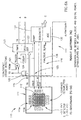
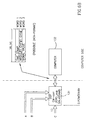
- Figs. 6a and 6b are a schematic diagram showing a system depicted generally as 110 comprising a sensor module 111 having an array of 512 pixels 112 constituted by silicon diodes which are responsive to an incident ⁇ -ray for producing a charge signal.
- the sensor module 111 may be part of a Compton camera for use in tomographic imaging of a patient's body.
- Such a Compton camera is provided with two separate detectors: one of which is a multilayer sensor whose multiple layers serve to increase the Compton effect and each of which is provided with its own independent readout circuit for enabling the data signal to be read out.
- the second detector which is not itself a feature of the invention, may be a similar pixel array or any other suitable sensor for absorbing the ⁇ -ray which emerges from the first detector.
- the ⁇ -ray gives up its residual energy in the second detector thereby allowing the angle of the ⁇ -ray to be calculated in known manner.
- the present invention is thus applicable primarily to the first detector in which the pixel arrays 112 are arranged into 16 groups of pixels each having 32 pixels.
- the sensor module 111 includes on-chip discrimination circuitry in respect of each of the 16 groups of pixels in the pixel array 112, in the form of a pair of application specific integrated circuits (ASICs) 113a and 113b which may, if desired, be combined in a single ASIC. Details of the ASICs 113a and 113b are given below with reference to Fig. 10 of the drawings.
- Respective output channels of the discrimination circuitry are fed to a readout circuit 114 for sequentially selecting a different group of pixels and coupling the pixels in the selected group to respective first and second data buses 115 and 116.
- the pixels in each group are fed to a multi-input discriminator so as to derive a composite signal which is fed to a corresponding data line in the first data bus 115.
- the composite signal level is derived from all of the pixels in the respective group and is HIGH if any of the pixels in the group is "active" and is otherwise LOW. Consequently, only one data line will be HIGH indicating which of the 16 groups of pixels is "active” whilst the other 15 data lines corresponding to the remaining 15 groups containing, in total, some 480 pixels, are LOW, showing that none of the 480 pixels is "active".
- the location of the one "active" pixel is very significantly narrowed down; although of course, at this stage, it is not yet known which of the 32 pixels in this group is the "active" pixel.
- All 16 data lines in the first data bus 115 are connected to respective inputs of a 16 input OR-gate 120 (constituting a first logic circuit) whose output is consequently HIGH (constituting a first logic level) if any one or more of the 16 data lines is HIGH indicating that the corresponding group is "active". If none of the 512 pixels in the sensor module 111 is "active", then the output of the OR-gate 120 is LOW (constituting a second logic level).
- several sensor modules may be assembled so as to form a multi-layer image sensor each having a plurality of sensor modules.
- Each sensor module has an associated OR-gate 120 and the output of the OR-gate in each module is fed to one input of a 2-input AND-gate 121 (constituting a second logic circuit) to whose second input is fed an output from a second detector (not shown). Consequently, the output of the AND-gate 121 in each sensor module is HIGH only if the outputs of at least one of the OR-gates 120 in the respective sensor module is HIGH, and at the same time the output of the second detector is HIGH.
- the AND-gate 121 thus allows time coincidence of charge emissions emanating from both the first and second detectors to be established in real time. A ⁇ -ray may strike the image sensor obliquely and if it is partially absorbed in one layer then its angle will change thus permitting its subsequent detection.
- a decoding circuit 122 is coupled to the first data bus 115 and is responsive to the composite signal on each of the data lines thereof for determining which of the data line is HIGH thereby establishing an identity of the active group.
- a a timing circuit 123 is coupled to the output of the OR-gate 120 via the AND-gate 121 and is responsive to the output of the OR-gate 120 being HIGH (i.e. the first logic level) for generating a time stamp corresponding to a time of creation of the first logic level which is substantially coincident with the pixel response.
- the second data bus 116 is constituted by an analog data line 126 which is coupled via a sequencer 127 (constituting a selection circuit) to each of the pixels in a selected one of the groups for receiving thereon respective signal levels of each of the pixels in the selected group.
- the sequencer 127 is responsive to a start signal which is fed to a start input thereof via the delay line 125 for cycling through the pixel addresses in the active group so as to output serially on the analog data line 126 an analog signal corresponding to the signal level of each pixel in turn in the active group.
- the analog data line 126 is coupled to an analog-to-digital converter (ADC) 130, the output of which is a digital signal representative of the signal level of the corresponding pixel in the active group.
- ADC analog-to-digital converter
- the digital signal output by the ADC 130 is fed to a digital signal processor (DSP) 131 (constituting a discriminating circuit) which is programmed to compare the signal level of each pixel in the selected group with a discriminating threshold so as to identify the active pixel as that pixel whose signal level exceeds the discriminating threshold.
- DSP digital signal processor
- the DSP 131 also functions as a common mode noise level determination circuit for determining an average common mode noise level associated with the 131 pixels in the selected group whose signal levels are not commensurate with an "active" pixel.
- the common mode noise levels of the 131 inactive pixels is averaged and then subtracted from the signal level of the "active" pixel so as to correct for common mode noise.
- the DSP 131 produces a digital data stream containing data representative of the module number, the active group identity, the active pixel identity, the time stamp of the active pixel and the common mode noise-corrected signal level thereof.
- the resulting digital data stream is then transmitted to a computer 132 where it is processed as required: this not being a feature of the present invention.
- the module number is a pre-programmed code, which is down-loaded into the corresponding sensor module 111 and which thus identifies from which sensor module a data signal was emitted.
- the time stamp specifies the time based on a common real time clock (not shown) at which a charge emission occurred by the identified pixel. These data are relevant when coincident data from the first detector is combined with the corresponding data from the second detector so as to calculate the location of the incident ⁇ -ray and its angle of incidence. It should, however, be noted that the time stamps are not used to establish time coincidence of a charge emission from the first and second detectors: this being established in real time using logic gates as explained above with reference to Figs. 6a and 6b of the drawings.
- Fig. 7 shows pictorially a multi-layer sensor 140 being part of a first detector for a Compton camera and having five parallel identical sensor planes each designated 141 and comprising an array of nine sensor modules 111 as described above with reference to Fig. 6a of the drawings.
- Each of the sensor modules 111 in each sensor plane 141 is coupled to a respective reading circuit 142, so that nine reading circuits are required for each sensor plane.
- Respective outputs 143 of each of the reading circuits 142 are coupled via a data bus 144 to a computer 145.
- a ⁇ -ray impinging on the sensor 140 has sufficient energy to penetrate through all the layers 141 thereof, but produces a charge data signal only if it is partially absorbed by a pixel in at least one sensor plane.
- the provision of multiple layers increases the probability that a Compton effect will occur in at least one pixel of the sensor. It should be noted that the same objective can also be realized by increasing the surface area of each sensor plane.
- Fig. 8 shows graphically three curves 150, 151 and 152 representing respective charge signals emanating at the same time t 0 and each having a different peak value V P .
- a time delay t D is fed via a delay line 125 to a latch in a sample and hold circuit (shown as 164 in Fig. 10) within the ASIC 113a so that the data signal generated by the "active" pixel may be sampled at a time delay t P after its generation.
- the time delay t D may be predetermined based on the value of ⁇ t and the peak tine t P which is known from the RC time-constant of the shaper, so that if the start of the signal at time t 0 is known, then the curve may be sampled exactly at the peak time t P so as to obtain the peak value V P .
- Figs. 9a and 9b show graphically a solution to the problem of time walk by means of which the desired compensation can be effected.
- Fig. 9a shows a typical integrated charge curve 155 having a known peak time t P .
- this in itself is not sufficient to measure accurately the peak value V P because it is first necessary to determine a reliable time origin t 0 using a threshold discriminator as explained above.
- the invention provides a second shaper having a very much faster time constant so as to produce a sharp curve 156 (shown in Fig. 9b) which crosses the threshold after a time ⁇ t very much less than the peak time t P of the slow shaper. Having thus determined from the curve 156 that the signal corresponds to pixel data and not the signal baseline level, the first curve 155 may be sampled after a time delay t D equal to t P - ⁇ t .
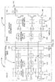
- Fig. 10 shows a detail of the reading circuit 142 illustrating the application of duplicated shapers having different time constants in order to compensate for time walk.
- each pixel 112 in a selected group is fed via a solder pad 159 to an integrator 160 formed by a preamplifier 161 having a feedback capacitor 162 and resistor 162'.
- the integrated output of the preamplifier 161 is filtered by a first CR-RC shaper 163 (constituting a slow shaper) and then passed to a sample and hold unit 164.
- the analog output of the sample and hold unit 164 is multiplexed by a multiplexer 165 so that the signal corresponding to each of the 132 pixels in each group can be sampled and processed.
- the pixel 112 is referenced in the first ASIC 113a for the sake of clarity only.
- the pixel 112 is contained within the sensor module 111 which is a physically distinct unit from the ASIC 113a and each of whose pixels 112 is hard-wired to the respective solder pad 159 within the ASIC 113a.
- the input circuit shown in either Fig. 4 or 5 is likewise connected to the same solder pad 159 and ensures that the current flowing through the feedback resistor 162' is maintained at its equilibrium value equal to the offset of the preamplifier 161.
- the output of the preamplifier 161 is also fed to a second CR-RC shaper 166 (constituting a fast shaper) having an integration time (i.e. peak time) which is in the order of ten times shorter than that of the first shaper 163.
- the output of the second shaper 166 is fed to a level discriminator 167 whose threshold is of sufficient magnitude to discriminate between a genuine signal and the signal baseline level.
- the output of the level discriminator 167 is fed to a monostable 168 whose output is coupled to the gate of a MOSFET 169.
- the monostable 168 is thus responsive to an "active" pixel within the respective group for producing a short trigger pulse for switching on the MOSFET 169.
- the MOSFETs 169 of each group are connected in wired OR configuration so that if any of the pixels in the selected group is "active" the combined output of the MOSFETs 169 will be HIGH.
- the second shaper 166 permits very fast discrimination in respect of an "active" pixel whereafter the slow integrated signal generated by the first shaper 163 may be accurately sampled after a constant delay time t D in order to establish its peak value V P .
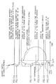
- Figs. 11a to 11f summarize the various signal levels associated with an "active" pixel all drawn according to a common time base.
- Fig. 11a shows the actual charge signal emitted by a pixel consequent to being struck by a ⁇ -ray.
- this signal is a sharp current pulse starting at time t 0 , almost instantaneously rising to a peak value and then trailing off to zero.
- Fig. 11b represents the corresponding waveform after pre-amplification.
- the preamplifier integrates the charge data signal so as to produce an analog voltage signal having a sharp change in level upon emission of the data signal.
- the sharp change in level defines the start time t 0 of the data signal.
- Figs. 11c and 11d show respectively the slow and fast shaped data signals.
- the shaped signal rises to a peak value V P at a time t P after the start time t 0 and then trails off to zero as shown by the dotted line.
- the waveform must be sampled and held at the time t P in order to capture the peak value V P .
- the fast shaped signal rises through the threshold alter a time interval ⁇ t following the start time t 0 .
- Fig. 11e shows the output of the monostable 168 (shown in Fig. 10) which is a sharp square wave pulse generated at time t 0 + ⁇ t and which is fed via the MOSFET 169 to the delay circuit 124 (shown in Fig. 6a) so as to trigger the delay circuit 124 whereby after a further delay time t D equal to t P - ⁇ t the slow integrated signal shown in Fig. 11c is sampled at its peak value V P .
- each pixel is effectively a diode.
- other semiconductor sensors may also be employed in which case the pixels are high resistive elements.
Landscapes
- Physics & Mathematics (AREA)
- Health & Medical Sciences (AREA)
- Life Sciences & Earth Sciences (AREA)
- General Physics & Mathematics (AREA)
- High Energy & Nuclear Physics (AREA)
- Molecular Biology (AREA)
- Spectroscopy & Molecular Physics (AREA)
- Engineering & Computer Science (AREA)
- Multimedia (AREA)
- Signal Processing (AREA)
- Other Investigation Or Analysis Of Materials By Electrical Means (AREA)
- Measurement Of Radiation (AREA)
- Investigating Or Analyzing Materials By The Use Of Electric Means (AREA)
- Nuclear Medicine (AREA)
Applications Claiming Priority (2)
| Application Number | Priority Date | Filing Date | Title |
|---|---|---|---|
| IL12787998 | 1998-12-31 | ||
| IL12787998A IL127879A0 (en) | 1998-12-31 | 1998-12-31 | Improved input circuit for a charge detector |
Publications (2)
| Publication Number | Publication Date |
|---|---|
| EP1016882A2 true EP1016882A2 (de) | 2000-07-05 |
| EP1016882A3 EP1016882A3 (de) | 2002-03-20 |
Family
ID=11072327
Family Applications (1)
| Application Number | Title | Priority Date | Filing Date |
|---|---|---|---|
| EP00300018A Withdrawn EP1016882A3 (de) | 1998-12-31 | 2000-01-05 | Ladungsdetektor-Ausgangsschaltung |
Country Status (4)
| Country | Link |
|---|---|
| EP (1) | EP1016882A3 (de) |
| JP (1) | JP2000206249A (de) |
| IL (1) | IL127879A0 (de) |
| NO (1) | NO996539L (de) |
Cited By (8)
| Publication number | Priority date | Publication date | Assignee | Title |
|---|---|---|---|---|
| FR2857545A1 (fr) * | 2003-07-08 | 2005-01-14 | Commissariat Energie Atomique | Dispositif de detection de rayonnement electromagnetique et de lecture d'un signal representatif du rayonnement detecte a dispositif de polarisation integre. |
| WO2006018692A3 (en) * | 2004-08-18 | 2006-07-06 | Uni Degli Studi Brescia | Apparatus and method for conditioning signals produced by physico-chemical sensors |
| EP2372098A2 (de) | 2009-12-23 | 2011-10-05 | Rolls-Royce plc | Ringförmige Füllerbaugruppe für einen Rotor einer Turbomaschine |
| WO2012036496A3 (ko) * | 2010-09-17 | 2012-06-07 | 주식회사 룩센테크놀러지 | Dc 누설 전류를 보상하는 전하 감지 증폭 회로, 이를 이용한 엑스선 독출 집적 회로 및 엑스선 센서 |
| JP2013039306A (ja) * | 2011-08-19 | 2013-02-28 | Toshiba Corp | X線コンピュータ断層撮影装置 |
| CN107238771A (zh) * | 2017-06-15 | 2017-10-10 | 中国汽车技术研究中心 | 一种电动汽车直流高压母线残余电能测量装置及方法 |
| CN113433584A (zh) * | 2021-06-28 | 2021-09-24 | 哈尔滨工业大学 | 可兼容电子收集和空穴收集的像素探测器中的像素电路 |
| EP4004604A4 (de) * | 2019-07-29 | 2023-04-19 | Shenzhen Xpectvision Technology Co., Ltd. | Verstärker für dunkelrauschkompensation |
Families Citing this family (4)
| Publication number | Priority date | Publication date | Assignee | Title |
|---|---|---|---|---|
| US7800439B2 (en) * | 2006-10-27 | 2010-09-21 | Ut-Battelle, Llc | High speed preamplifier circuit, detection electronics, and radiation detection systems therefrom |
| JP6214031B2 (ja) * | 2013-07-19 | 2017-10-18 | 国立研究開発法人理化学研究所 | 放射線検出器のための信号データ処理方法、信号データ処理装置、および放射線検出システム |
| US10162066B2 (en) * | 2017-02-06 | 2018-12-25 | General Electric Company | Coincidence-enabling photon-counting detector |
| US20260072183A1 (en) * | 2022-08-31 | 2026-03-12 | Dai Nippon Printing Co., Ltd. | Detecting apparatus and radiation identification apparatus |
Family Cites Families (2)
| Publication number | Priority date | Publication date | Assignee | Title |
|---|---|---|---|---|
| US4672207A (en) * | 1985-08-21 | 1987-06-09 | The United States Of America As Represented By The United States Department Of Energy | Readout system for multi-crystal gamma cameras |
| US4893018A (en) * | 1986-05-21 | 1990-01-09 | Kabushiki Kaisha Toshiba | Radiation detecting circuit including positional error calibrator |
-
1998
- 1998-12-31 IL IL12787998A patent/IL127879A0/xx unknown
-
1999
- 1999-12-28 JP JP11373941A patent/JP2000206249A/ja active Pending
- 1999-12-29 NO NO996539A patent/NO996539L/no not_active Application Discontinuation
-
2000
- 2000-01-05 EP EP00300018A patent/EP1016882A3/de not_active Withdrawn
Cited By (12)
| Publication number | Priority date | Publication date | Assignee | Title |
|---|---|---|---|---|
| FR2857545A1 (fr) * | 2003-07-08 | 2005-01-14 | Commissariat Energie Atomique | Dispositif de detection de rayonnement electromagnetique et de lecture d'un signal representatif du rayonnement detecte a dispositif de polarisation integre. |
| WO2005006741A1 (fr) * | 2003-07-08 | 2005-01-20 | Commissariat A L'energie Atomique | Dispositif de detection de rayonnement electromagnetique et de lecture d'un signal representatif du rayonnement detecte a dispositif de polarisation integre. |
| WO2006018692A3 (en) * | 2004-08-18 | 2006-07-06 | Uni Degli Studi Brescia | Apparatus and method for conditioning signals produced by physico-chemical sensors |
| EP2372098A2 (de) | 2009-12-23 | 2011-10-05 | Rolls-Royce plc | Ringförmige Füllerbaugruppe für einen Rotor einer Turbomaschine |
| WO2012036496A3 (ko) * | 2010-09-17 | 2012-06-07 | 주식회사 룩센테크놀러지 | Dc 누설 전류를 보상하는 전하 감지 증폭 회로, 이를 이용한 엑스선 독출 집적 회로 및 엑스선 센서 |
| JP2013039306A (ja) * | 2011-08-19 | 2013-02-28 | Toshiba Corp | X線コンピュータ断層撮影装置 |
| CN107238771A (zh) * | 2017-06-15 | 2017-10-10 | 中国汽车技术研究中心 | 一种电动汽车直流高压母线残余电能测量装置及方法 |
| CN107238771B (zh) * | 2017-06-15 | 2023-11-03 | 中国汽车技术研究中心 | 一种电动汽车直流高压母线残余电能测量装置及方法 |
| EP4004604A4 (de) * | 2019-07-29 | 2023-04-19 | Shenzhen Xpectvision Technology Co., Ltd. | Verstärker für dunkelrauschkompensation |
| US12146999B2 (en) | 2019-07-29 | 2024-11-19 | Shenzhen Xpectvision Technology Co., Ltd. | Amplifier for dark noise compensation |
| CN113433584A (zh) * | 2021-06-28 | 2021-09-24 | 哈尔滨工业大学 | 可兼容电子收集和空穴收集的像素探测器中的像素电路 |
| CN113433584B (zh) * | 2021-06-28 | 2022-11-04 | 哈尔滨工业大学 | 可兼容电子收集和空穴收集的像素探测器中的像素电路 |
Also Published As
| Publication number | Publication date |
|---|---|
| JP2000206249A (ja) | 2000-07-28 |
| IL127879A0 (en) | 1999-10-28 |
| NO996539D0 (no) | 1999-12-29 |
| NO996539L (no) | 2000-07-03 |
| EP1016882A3 (de) | 2002-03-20 |
Similar Documents
| Publication | Publication Date | Title |
|---|---|---|
| US7512210B2 (en) | Hybrid energy discriminating charge integrating CT detector | |
| US6509565B2 (en) | Discriminator circuit for a charge detector | |
| US8148695B2 (en) | Nuclear medical diagnosis apparatus | |
| US6657200B2 (en) | Readout system for solid-state detector arrays | |
| US8247780B2 (en) | High density, proportional-mode, APD arrays for individual scintillator readout in PET applications | |
| US6153882A (en) | Method and system for reading a data signal emitted by an active pixel in a sensor | |
| EP3049827B1 (de) | Gemischtes photonenzählendes datenerfassungssystem | |
| EP1016882A2 (de) | Ladungsdetektor-Ausgangsschaltung | |
| US9869781B2 (en) | Active pulse shaping of solid state photomultiplier signals | |
| RU2010130183A (ru) | Интегрирующий детектор с регистрацией счета | |
| CN101680955A (zh) | 谱光子计数探测器 | |
| EP2176684A2 (de) | Vorrichtung und verfahren zur erzeugung zählbarer impulse aus auftreffenden röntgenphotonen sowie entsprechende abbildungsvorrichtung | |
| WO2007099395A2 (en) | Methods and systems for medical imaging | |
| JPH1172564A (ja) | ガンマカメラシステム | |
| FI114270B (fi) | Elektroninen säteilykuvantamisjärjestelmä | |
| US7518102B2 (en) | Calibration method and apparatus for pixilated solid state detector | |
| CN114902301B (zh) | 文件认证 | |
| TWI769263B (zh) | X射線檢測器,用於檢測x射線之方法,x射線系統,x射線貨物掃描或非侵入式檢查系統,x射線全身掃描系統,x射線計算機斷層掃描系統,以及電子顯微鏡 | |
| US4413183A (en) | Gamma camera | |
| WO2006080004A2 (en) | Method and system for x-ray radiation imaging | |
| TWI849518B (zh) | 成像系統及利用其的方法 | |
| US20220354444A1 (en) | Imaging system using x-ray fluorescence | |
| US11112511B2 (en) | Radiation detector and compton camera | |
| US7564040B2 (en) | Device for correcting a signal derived from a detector | |
| CN119156551A (zh) | 时间延迟求和模式下的光子计数检测器 |
Legal Events
| Date | Code | Title | Description |
|---|---|---|---|
| PUAI | Public reference made under article 153(3) epc to a published international application that has entered the european phase |
Free format text: ORIGINAL CODE: 0009012 |
|
| AK | Designated contracting states |
Kind code of ref document: A2 Designated state(s): AT BE CH CY DE DK ES FI FR GB GR IE IT LI LU MC NL PT SE |
|
| AX | Request for extension of the european patent |
Free format text: AL;LT;LV;MK;RO;SI |
|
| RIN1 | Information on inventor provided before grant (corrected) |
Inventor name: NYGARD, EINAR |
|
| PUAL | Search report despatched |
Free format text: ORIGINAL CODE: 0009013 |
|
| RIC1 | Information provided on ipc code assigned before grant |
Free format text: 7G 01T 1/29 A, 7G 01T 1/17 B |
|
| AK | Designated contracting states |
Kind code of ref document: A3 Designated state(s): AT BE CH CY DE DK ES FI FR GB GR IE IT LI LU MC NL PT SE |
|
| AX | Request for extension of the european patent |
Free format text: AL;LT;LV;MK;RO;SI |
|
| STAA | Information on the status of an ep patent application or granted ep patent |
Free format text: STATUS: THE APPLICATION HAS BEEN WITHDRAWN |
|
| 18W | Application withdrawn |
Withdrawal date: 20020429 |