EP1016980A2 - Système d'interconnexion distribué à noeuds de commutation intégrés - Google Patents
Système d'interconnexion distribué à noeuds de commutation intégrés Download PDFInfo
- Publication number
- EP1016980A2 EP1016980A2 EP99309766A EP99309766A EP1016980A2 EP 1016980 A2 EP1016980 A2 EP 1016980A2 EP 99309766 A EP99309766 A EP 99309766A EP 99309766 A EP99309766 A EP 99309766A EP 1016980 A2 EP1016980 A2 EP 1016980A2
- Authority
- EP
- European Patent Office
- Prior art keywords
- interconnection network
- fabrics
- fabric
- stage
- concentrator
- Prior art date
- Legal status (The legal status is an assumption and is not a legal conclusion. Google has not performed a legal analysis and makes no representation as to the accuracy of the status listed.)
- Granted
Links
Images




Classifications
-
- H—ELECTRICITY
- H04—ELECTRIC COMMUNICATION TECHNIQUE
- H04L—TRANSMISSION OF DIGITAL INFORMATION, e.g. TELEGRAPHIC COMMUNICATION
- H04L49/00—Packet switching elements
- H04L49/15—Interconnection of switching modules
-
- H—ELECTRICITY
- H04—ELECTRIC COMMUNICATION TECHNIQUE
- H04L—TRANSMISSION OF DIGITAL INFORMATION, e.g. TELEGRAPHIC COMMUNICATION
- H04L49/00—Packet switching elements
- H04L49/10—Packet switching elements characterised by the switching fabric construction
- H04L49/111—Switch interfaces, e.g. port details
-
- H—ELECTRICITY
- H04—ELECTRIC COMMUNICATION TECHNIQUE
- H04L—TRANSMISSION OF DIGITAL INFORMATION, e.g. TELEGRAPHIC COMMUNICATION
- H04L49/00—Packet switching elements
- H04L49/10—Packet switching elements characterised by the switching fabric construction
-
- H—ELECTRICITY
- H04—ELECTRIC COMMUNICATION TECHNIQUE
- H04L—TRANSMISSION OF DIGITAL INFORMATION, e.g. TELEGRAPHIC COMMUNICATION
- H04L49/00—Packet switching elements
- H04L49/15—Interconnection of switching modules
- H04L49/1515—Non-blocking multistage, e.g. Clos
- H04L49/1523—Parallel switch fabric planes
Definitions
- This invention relates in general to computer systems, and in particular, to a distributed multi-fabric interconnect for massively parallel processing computer systems.
- An interconnection network is the key element in a Massively Parallel Processing (MPP) system that distinguishes the system from other types of computers.
- An interconnection network, or just interconnect refers to the collection of hardware and software that form the subsystem through which the processors communicate with each other.
- An interconnect is comprised of Processor/Network (P/N) interfaces and one or more switching fabrics.
- a switching fabric comprises a collection of, switching elements, or switches, and links.
- Each switching element contains a minimum of three I/O ports: two or more inputs and one or more outputs, or one or more inputs and two or more outputs.
- Said element also contains a means for dynamically establishing arbitrary connections between inputs and outputs under the control of a routing mechanism.
- Each link establishes a permanent connection between the output of one switching element (or P/N interface) and the input of another.
- the pattern of connections formed by links and switches define the topology of the fabric.
- the performance of the interconnect is either limited by the speed of the links between the switches or the speed of the switches themselves.
- Current semiconductor technology limits the speed of the links and the physical distance between the switching elements.
- the speed of the switches is limited by semiconductor technology and the complexity of the design.
- the scalability of the MPP system is also an important characteristic. Not only must connectivity scale, but performance must scale linearly as well.
- the MPP system size demanded by customers can vary from two to 1024 or more processing nodes, where each node may contain one or more processors. It is essential that the interconnect be able to grow in size incrementally. It is undesirable but common for MPP interconnects to double in size to accommodate the addition of one processing node as the total number of ports required crosses powers of two (e.g., an interconnect with 128 ports is required to support 65 processing nodes, which is at least twice as much hardware as 64 nodes require, depending on the topology used).
- MPP systems are typically comprised of large collections of processor/memory subsystems made by other manufacturers. Access to the processor is limited to the provided I/O bus, and it is generally no longer possible to gain access via the processor/memory bus.
- the I/O bus typically operates at a fraction of the speed of the processor/memory bus; however, multiple I/O busses are often provided. This situation favors interconnects that exploit parallelism rather than single, very high bandwidth interconnects.
- the first is centralized, in which all switching fabric hardware is housed in one physical location. Cables must be run from the P/N interface in each processing node to each fabric in the interconnect. In cases where there is more than one fabric, usually for providing fault tolerance, each fabric is centralized with respect to the processing nodes and independent of the other. Providing more fabrics using this arrangement multiplies all the hardware, cables and cost.
- the other approach is distributed, in which portions of the switching fabric are physically distributed among the processing nodes.
- An example of this is the Y-Net interconnect used in the TeradataTM DBC 1012 and NCRTM 3600 systems. This is also a popular arrangement for mesh and hypercube interconnects.
- each of the individual submodules and cables are duplicated. Since the packaging typically allocates a fixed amount of space for the portion of the fabric that coexists with each processing node, replicating fabrics to increase performance requires a redesign of the system packaging. In the case of typical mesh and hypercube interconnects, one switch is an integral part of the processor electronics, and is often co-located on the same board. Replicating the fabric is completely impractical, requiring the redesign of boards and packaging.
- the present invention resides in an interconnection network comprising a plurality of identical fabrics for interconnecting a plurality of processing nodes for communication therebetween, each of the fabrics comprised of at least one stage, each stage comprised of a plurality of switching elements, one or more of the switching elements from a first stage of each of the fabrics being combined together in at least one concentrator, the concentrator allowing all links from each processor to the fabrics to be combined into a single cable coupled to the concentrator.
- the invention resides in a massively parallel processing system comprising the above interconnection network.
- the invention also resides in a concentrator for the above interconnection network.
- the present invention provides a method for partitioning the switching elements of multiple fabrics, so that many links can be combined into single cables, thereby enabling higher density packaging and making the implementation of multiple fabrics practical.
- the partitioning method disclosed is applicable to any multistage interconnect constructed from a x b bidirectional switching elements, where a >1, b >0 or a >0, b >1.
- one or more of the switching elements from the first stage of each of several identical fabrics are physically packaged on to the same board called a concentrator, and these concentrators are physically distributed among the processing nodes.
- This concentrator approach allows all the links from each processing node to a concentrator, each of which need to be connected to different fabrics, to be combined into a single cable. Furthermore, it allows all the links emanating from a single switching element in the first stage to be combined into a single cable to be connected to the second and subsequent stages of that fabric in larger configurations.
- each fabric can be implemented independently of other fabrics in a centralized location. This partitioning of the collection of all the fabrics in the interconnect is what leads to all the benefits that have been described.
- the invention is advantageous in that it leads to reduction of the cable count in MPP systems, and also eases the installation effort. Moreover, implementation of the interconnect is distributed, so that the switching hardware can consume otherwise unused space, power and cooling resources by being co-located with processor hardware.
- a typical MPP system can be considered to be comprised of an interconnection network, a number of processing nodes, and mass storage attached to the nodes.
- storage can be considered just another node from the point of view of the interconnect.
- the partitioning method taught by this invention is broadly applicable to a very large class of interconnects. To characterize those for which it is suitable, the following parameters are defined.
- the basic building block is assumed to be an a port by b port, or a x b , bidirectional switching element, where a> 1, b >0 (or a >0, b> 1). By convention, it is assumed that, logically, the a ports are on the left side of the switching element and the b ports are on the right side of the switching element.
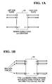
- FIG. 1A illustrates a generic bidirectional a x b crossbar switching element 100 and FIGS. 1B, 1C, and 1D illustrate three possible implementations of the element.
- Each port of the element 100 is a bidirectional port that can either be comprised of (1) a single physical port that can move data in either direction under the control of an associated direction control line and is designated TYPE I (FIG. 1B); or (2) can be implemented as independent input and output ports and is designated TYPE II (FIGS. 1C and 1D).
- TYPE II switching elements can be implemented in two different ways.
- the second designated TYPE IIb (FIG. 1D) uses an ( a+b ) x ( a+b ) unidirectional switching element. It can be arranged to behave as an a x b bidirectional switching element. To do so, a input ports and a output ports are associated with the left side and b input ports and b output ports are associated with the right side.
- the second form simply has a + b bidirectional ports, a on the left and b on the right. This implementation allows a message's path to turn around at any stage because any input port, i , can be connected to output port, i .
- FIG. 2 illustrates a fabric 200 constructed from a x b switching elements, wherein a , b , and n are positive integers, a + b ⁇ 3.
- a fabric 200 can take one of two forms.
- the first form uses only the left side ports of the left most stage for external connection to processing (or other) nodes.
- the right side ports of the right most stage use a "loop-back" mode, automatically sending any message reaching the right side of the fabric back in the direction from which it came.
- All messages in such a fabric 200 implemented with TYPE IIa switching elements will always pass through the loop-back connections in the right most stage.
- these fabrics 200 there are as many paths between any pair of left side ports as there are right side ports. Hence, these fabrics 200 are highly fault tolerant. If TYPE IIb switching elements are implemented, messages in FORM I fabrics 200 may turn around before reaching the loop-back stage.
- the second form, FORM II use both sides of the fabric 200 for external connection to processor (or other) nodes. When used this way, it is more efficient to use either TYPE I or TYPE IIb switching elements which allow early turn-around to minimize the path length of messages entering and exiting the same side of the fabric 200.
- any interconnection network with K fabrics, K >1, where the fabrics use a multistage topology constructed from the a x b switching elements (as defined above), can benefit from the partitioning method described herein.
- a very useful and practical to implement subset of all possible such interconnects can be characterized as follows.
- N log a ( N ) , numbered from 0 to n -1, left to right.
- the first stage of each fabric requires N/ a or a n -1 switching elements, numbered from 0 to a n -1 -1 (see FIG. 2). It has a n left side ports and a n -1 b right side ports.
- the i th stage, 0 ⁇ i ⁇ n has a n-i -1 b i switching elements, a n-i b i left side ports and a n-i -1 b i +1 right side ports.
- the n -1 st or last stage has b n -1 switching elements, ab n -1 left side ports and b n right side ports. (Depending on the form of the interconnect, there are either b" loop-back points, or b n I/O ports for external connection to processor or other nodes.)
- the first method is by (Stage : Level) and the second method is by the triplet (Stage : Switch-Element-Number : Switch-Element-Port-Number).
- X right / i represent the level of a right side port in the i th stage, then X can be represented by a combination of a -ary and b -ary digits as follows.
- Such a notation is referred to as a mixed radix representation.
- the number of right side ports in stage j must be equal to the number of left side ports in stage j +1 so that a permutation of the links can be formed. That is equivalent to determining that the maximum value representable by each X is the same.
- MAX( X right / j ) MAX( X left / j +1), 0 ⁇ j ⁇ n -1, must be true.
- the following conversion formula can be used to verify that this is true:
- Base r is typically 10, but any base could be used.
- the maximum value of a four digit base 10 number is represented by setting all the digits to "9”
- the notation ( i : ⁇ i -1 ... ⁇ 1 ⁇ 0 ⁇ n - i -1 ... ⁇ 1 ⁇ 0 ) left is used, and by the second method, ( i : ⁇ i -1 ... ⁇ 1 ⁇ 0 ⁇ n - i -1 ... ⁇ 1: ⁇ 0 ) left .
- the first method specifies ( i : ⁇ n - i -2 ... ⁇ 1 ⁇ 0 ⁇ 1 ... ⁇ 1 ⁇ 0 ) right
- the second ( i : ⁇ n - i -2 ... ⁇ 1 ⁇ 0 ⁇ i ... ⁇ 1 : ⁇ 0 ) right
- the second ( i : ⁇ n - i -2 ... ⁇ 1 ⁇ 0 ⁇ i ... ⁇ 1 : ⁇ 0 ) right .
- left side port numbers must end with an ⁇ radix digit and right side port numbers must end with a ⁇ radix digit. Because of this one to one relationship, where it is not essential for clarity, the "left" and “right” designations are omitted from some mixed radix representations.
- each radix is grouped together and numbered from 0 to the number of digits required minus one. However, except for the least significant digit, all other digits can appear in the representation in any order, but their quantity cannot change.
- any multistage interconnect must be constructed in such a way that the address (level) of the entry port can be "transformed" into the address of the exit port. There is a one-to-one relationship between the transformation required and the path taken. When addresses are represented symbolically, the effect of passing through a switching element or moving from one stage to the next can be readily characterized.
- this is equivalent, for example, to transforming ( i : ⁇ i -1 ... ⁇ 1 ⁇ 0 ⁇ n - i -1 ... ⁇ 1 ⁇ 0 ) left into ( i : ⁇ i -1 ... ⁇ 1 ⁇ 0 ⁇ n - i -1 ... ⁇ 1 ⁇ i ) right , that is, the least significant digit is converted from an ⁇ to a ⁇ .
- the higher order digits are preserved. Depending on the actual topology of the fabric, the higher order digits will be in some radix order, not necessarily that shown in this example. Whatever the order is, it will be preserved.
- the permutation connections between stages must be designed so that every a in the original address is moved to the least significant digit position, one per stage. Upon exit from the right most stage of the fabric, every ⁇ in the original address will have been transformed into a ⁇ . (Assuming the implementation supports turning around at any stage, turn-around is allowed whenever the unprocessed higher order digits of the entry address match the same digits of the exit address, and there is no need to process those digits.)
- the pattern of connections between each Stage can be completely specified by permuting the digits of the Level number.
- the total set of switching element right side ports numbered ( i : ⁇ n -1 / n - i -2... ⁇ i +2 / 1 ⁇ i +1 / 0 ⁇ i / i ...
- ⁇ 1 / 1 ⁇ 0 / 0) right are connected to the switching element left side ports numbered ( i +1: PERMUTE n / i ⁇ ( ⁇ n -1 / n - i -2... ⁇ i +2 / 1 ⁇ i +1 / 0 ⁇ i / i ... ⁇ 1 / 1 ⁇ 0 / 0) right ⁇ ) left .
- the permutation function is subscripted with an " i " to indicate that the function is associated with a specific Stage, and typically, is different in each Stage.
- the " n " superscript refers to the number of Stages in the interconnect. Superscripts have been added to indicate digit position.
- n digits There are always n digits numbered from 0 to n -1.
- PERMUTE n / i must rearrange the digits in such a way that the least significant digit is always an ⁇ , meeting the requirement for representing a left side level and assuring that a new ⁇ is presented at each stage for transformation by the switching elements there into a ⁇ .
- two digit permutations that start with ( ⁇ n -1 / n - i -2... ⁇ i +2 / 1 ⁇ i +1 / 0 ⁇ i / i ... ⁇ 1 / 1 ⁇ 0 / 0) right and both place ⁇ i +1 / 0 in the least significant digit position are ( ⁇ i / i ... ⁇ 1 / 1 ⁇ 0 / 0 ⁇ n -1 / n - i -2... ⁇ i +2 / 1 ⁇ i +1 / 0) left and ( ⁇ n -1 / n - i -2... ⁇ i +2 / 1 ⁇ i / i ... ⁇ 1 / 1 ⁇ 0 / 0 ⁇ i +1 / 0) left .
- they cause the same digit to be processed by switching elements in the i +1 st stage, they have significantly different topologies.
- a tracer can be used to track the movement of digits caused by applying a permutation.
- a tracer is constructed of a sequence of n digits which each represent the value of their original position in a mixed radix number.
- a tracer is simply the sequence of superscripts shown in the mixed radix representations, i.e., [( n -1),( n -2) ,... i,...2,1,0].
- Right side port numbers in stage 2 are represented by ( ⁇ 4 / 1 ⁇ 3 / 0 ⁇ 2 / 2 ⁇ 1 / 1 ⁇ 0 / 0) right .
- Digit number 3 (the fourth most significant digit) is ⁇ 0 .
- the two permutations are ( ⁇ 2 / 2 ⁇ 1 / 1 ⁇ 0 / 0 ⁇ 4 / 1 ⁇ 3 / 0) left and ( ⁇ 4 / 1 ⁇ 2 / 2 ⁇ 1 / 1 ⁇ 0 / 0 ⁇ 3 / 0) left :
- the input tracer is [43210] (commas are omitted from the tracer when each digit position can be represented by a single decimal digit).
- Tracers can be used in different ways.
- One way is to illustrate the effect of a single permutation used in one stage, say stage i .
- the input tracer is "injected" at the right side ports of stage i and the resultant output tracer appears at the left side ports of stage i +1.
- the third use of a tracer is to inject it into the left side ports of stage 0 and track its transformation as it passes through switching elements and the permutations between stages until it emerges from the right side ports in stage n -1.
- the tracer that emerges from one stage serves as input to the next, it is not reinitialized to be an input tracer.
- a tracer that started in stage 0 may look different when it arrives at the left side ports in stage i +1 than one that originated at the right side ports in stage i .
- a and b can take three forms, each of which defines a different class of interconnect. If a ⁇ b , a trapezoidal shaped fabric is formed in which there are b n paths between every pair of a n fabric left side ports. When implemented as a FORM I fabric, there are more paths internal to the fabric than external. Assuming a message routing scheme that exploits this property, this class of fabrics would have less internal contention among messages which would produce lower latency and higher throughput. A FORM II version of this class would be suitable for an architecture in which storage is attached to the interconnect. In cases in which the ratio of storage nodes to processing nodes is greater than one, processor nodes would be attached to the left side and storage nodes to the right. If the converse were true, the attachment sides would be reversed.
- the NCR Y-Net is an example of a FORM I binary tree.
- the switching elements are "square" having equal numbers of ports on each side and thus, produce square fabrics.
- This class is a special case, because all digits used in numbers representing levels have the same arity or radix. This leads to simplification of the notation needed to describe the characteristics of this class of fabrics.
- the first is preferred because ⁇ 1 does not change position. That implies the worst case physical "distance" the links must span is minimal.
- PERMUTE 3 / 1 ⁇ X ⁇ There are only two legal possibilities for PERMUTE 3 / 1 ⁇ X ⁇ , but which two depends on what was selected for PERMUTE 3 / 0 ⁇ X ⁇ . If either (I) or (II) was selected, so the mixed radix representation of the right side port level in stage 0 is of the form ⁇ , then PERMUTE 3 / 1 ⁇ 0 ⁇ 1 ⁇ 0 ⁇ is either ⁇ 1 ⁇ 0 ⁇ 0 ([1 ⁇ 0 ⁇ 2 ⁇ ]) or ⁇ 0 ⁇ 1 ⁇ 0 ([0 ⁇ 1 ⁇ 2 ⁇ ]), neither of which has any particular advantage over the other.
- the form of the mixed radix representation for the right side level number i.e. the order in which the higher order (>0) digits appear at the right side ports, has a definite bearing on the topology generated in this stage. This is made clear by the tracers which track the movement of the digits. For example, even though ⁇ 1 ⁇ 0 ⁇ 0 is a desired form of left side address (of switching elements in stage i +1) for all four possible PERMUTE 3 / 0 ⁇ X ⁇ permutations, if the form of right side address (of switching elements in stage i ) is ⁇ 0 ⁇ 1 ⁇ 0 , tracer [1 ⁇ 0 ⁇ 2 ⁇ ] results.
- the underlined digits show the order in which the ⁇ 's are processed, i.e., 0, 2, 1.
- X 0 is the level of a right side port in stage 0 and Y 0 is the level of a left side port in stage 1, then they each have (2) 2 •3 or 12 possible values that range from 0 10 to 11 10 (subscripts on numbers indicate their base or radix).
- X 0 is represented in mixed radix notation by ( ⁇ 1 ⁇ 0 ⁇ 0 ) and Y 0 by ( ⁇ 0 ⁇ 0 ⁇ 1 ).
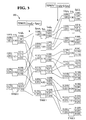
- FIG. 3 illustrates an example of a three stage fabric 300 constructed from 2 x 3 switching elements.
- every port level and switching element level is numbered in both decimal and mixed radix notation, wherein the mixed radix notation is shown in parentheses.
- the radix type for each number is shown at the top of the stages in FIG. 3. Notice that in each stage, the first two digits of every left side and right side port level are identical to the two digits representing the level of the switching element to which they connect. The least significant digit of left side ports is always an a and of the right side, a ⁇ .
- each processing node has K bidirectional links connecting it to the interconnect, with one link per fabric. Assuming the interconnect is implemented in a centralized fashion this provides an opportunity to consolidate the links into fewer cables (possibly one) depending on the value of K and the number of bidirectional links per cable, W , as selected technology permits.
- the number of cables per node, C is K/W . Assume all the links associated with a node are bundled into a trunk, then each node side trunk, or N-trunk, contains C N-trunk cables.
- the problem with this approach is that it is impractical to distribute the K links to K different fabrics and at the same time implement the fabrics so that they scale up to very large numbers of ports, even for nominal values of K (e.g., as few as 4).
- the solution is to partition the interconnect so that each switching element j 0 , 0 ⁇ j 0 ⁇ a n -1 in stage 0 is physically located with every other corresponding switching element j 0 from each other fabric. This creates a n -1 concentrators. Each concentrator has a incoming N-trunks, each trunk containing K links on the left side and K outgoing concentrator-trunks, or C-trunks, each containing b links, on the right. This is illustrated in FIG.
- the crux of this is that all of the links in a C-trunk go to the same fabric. That means the remaining stages of each fabric can be implemented and physically packaged independent of the other fabrics.
- one function of a concentrator 400 is to accept N-trunks from multiple nodes and regroup them into multiple C-trunks that each connect to different fabrics.
- the concentrators 400 are also K self-contained fabrics for up to a nodes.
- one concentrator is the entire interconnect.
- the concentrators reduce the number of cables needed to link clusters of nodes and concentrators to the centralized portion of the interconnect. If packaging constraints don't permit housing all K switching elements in one concentrator, multiple concentrators can be employed.
- the concentrators require a relatively small volume and can be co-located with the processing nodes. If C N-trunk > 1 or C C-trunk > 1, it may be appropriate to distribute the switching elements among C N-trunk or C C-trunk concentrators.
- the key point is that, technology permitting, there is the opportunity to reduce node cables by a factor of K and concentrator-to-central-switch cables by a factor of b. Since it is the connectors on the cables that tend to limit packaging density, this also enables higher density packaging of each fabric.
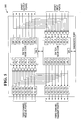
- the BiSN 500 of FIG. 5 is a TYPE IIa switching element (see FIG. 1C) and includes Fibre Channel Receive Ports (labeled as FC-Rx), Fibre Channel Transmit Ports (labeled as FC-Tx), Input Port Logic (labeled as IPLx), Output Port Logic (labeled as OPLx), Diagnostic Port Logic (labeled as DPL), BYNETTM Output Ports, and BYNETTM Input Ports.
- Selectable loop-back connections are provided internally, as illustrated in FIG. 5.
- some of the links that traverse short distances are parallel byte wide paths, while those that traverse longer distances are serial and use high speed Fibre Channel physical layer components and protocol.
- crossbar switches are cascaded in multiple stages to achieve the expanded connectivity for any number of processing nodes required by the system size. For example, one fabric in a system of 64 nodes would require 2 stages of 8 crossbar ASICs (16 crossbar ASICs) and one fabric in a system of 512 nodes would require 3 stages of 64 crossbar ASICs each (192 crossbar ASICs).
- crossbar switches are connected with a topology that allows communication between any two end points possible according to the methods described earlier.
- Current packaging technology requires the interconnect to be partitioned among multiple printed circuit boards, back planes and cabinets.
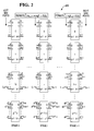
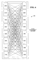
- FIG. 6 illustrates a two stage interconnect 600 implementing a folded banyan topology, which shows the typical logical interconnect 600 wiring pattern of a 64 port MPP fabric.
- FIG. 7 shows the logical connection between a processing node 700 and four fabrics 702.
- the concentrator solves this problem by transforming the grouping of links from multiple fabrics per cable to multiple links from the same fabric per cable. This then allows the portion of each fabric beyond the first stage to be packaged independently of the others.
- the interconnect in a large system resides in multiple cabinets connected together with cables.
- a 512 node system required 8 cabinets for one fabric.
- the physical dimension of the interconnect networks expands significantly.
- the expanded dimension may make the distance between the processing node and the interconnect stretch beyond the limits permitted by the technology.
- the number of cables between the interconnect and the processing nodes also increases as a multiple of the number of fabrics.
- the present invention reduces the number of cabinets and the cable counts by distributing the first stage of the interconnect networks.
- the 8x8 crossbar switches of the first stage of each fabric can be located on a new board type called a concentrator. Because the concentrator is small, it can occupy a chassis in the processor cabinet for an 8 node system or in a separate cabinet of multiple concentrators for the larger system .
- FIG. 8 illustrates the partitioning of switches from multiple fabrics 800 to form a concentrator 802, and also shows the logical connections between a processing node 804 and the four fabrics 800.
- the dotted box representing the concentrator 802 separates the switch nodes labeled BISN0 in each fabric 800 and places them on one concentrator 802 board.
- the cables (labeled as A, B, C, D) from the processing node 804 to the concentrator 802 can now be bundled together to reduce the number of individual cables. This is possible because all cables come from the same physical source (the processing node 804) and terminate at the same physical destination (the concentrator 802).
- the 8 outputs from switch node BISN0 of each fabric 800 can also be bundled into one cable to go to the next stage. This distribution of the first stage replaces 4 long cables between the processing node 804 and the first stages of the four fabrics 800 with one cable. It also replaces the 8 cables between the first stage and the second stage with a single cable.
- FIG. 9 illustrates a four fabric concentrator 900 with 8x8 switching elements 902, including the arrangement of crossbar switches and wiring connection on the concentrator 900.
- the four individual cables connecting the processing node 904 and the first stage switching elements 902 of the four fabrics (not shown) are now bundled into one cable 906 resulting in a 4-to-1 reduction in cables.
- the bundles are redistributed and routed to the four crossbar switches 902 comprising the first stages of the four fabrics.
- the outputs of each switch node 902 are bundled together at 908 to connect to the second stage resulting in an 8-to-1 reduction in cables.
- FIG. 10 illustrates the logical connection of an eight node 1000 cluster communicating with a single concentrator 1002 for four fabrics (not shown). Each of the nodes 1000 uses a different adapter 1004 to communicate with a different one of the fabrics.
- FIG. 11 shows the arrangement of crossbar switches 1100 and wiring connection for the second stage of a 64x64 port fabric.
- the second stage is comprised of 8 different switching elements 1100 that communicate with 8 different concentrators (not shown) via 8 bidirectional links per connector 1102.
- the switching elements 1100 are paired together into four printed circuit boards 1104 that communicate with each other through a back plane 1106.
- each fabric is constructed from a x b switching elements, a >1, b >0 (or a >0, b >1).
- the interconnects most practical to implement are those constructed using the large class of topologies as taught above, the technique to be described is applicable to any multistage interconnect.
Landscapes
- Engineering & Computer Science (AREA)
- Computer Networks & Wireless Communication (AREA)
- Signal Processing (AREA)
- Data Exchanges In Wide-Area Networks (AREA)
- Multi Processors (AREA)
- Small-Scale Networks (AREA)
- Structure Of Telephone Exchanges (AREA)
Applications Claiming Priority (2)
| Application Number | Priority Date | Filing Date | Title |
|---|---|---|---|
| US09/218,954 US6473827B2 (en) | 1998-12-22 | 1998-12-22 | Distributed multi-fabric interconnect |
| US218954 | 1998-12-22 |
Publications (3)
| Publication Number | Publication Date |
|---|---|
| EP1016980A2 true EP1016980A2 (fr) | 2000-07-05 |
| EP1016980A3 EP1016980A3 (fr) | 2003-03-19 |
| EP1016980B1 EP1016980B1 (fr) | 2007-02-28 |
Family
ID=22817174
Family Applications (1)
| Application Number | Title | Priority Date | Filing Date |
|---|---|---|---|
| EP99309766A Expired - Lifetime EP1016980B1 (fr) | 1998-12-22 | 1999-12-06 | Système d'interconnexion distribué à noeuds de commutation intégrés |
Country Status (3)
| Country | Link |
|---|---|
| US (1) | US6473827B2 (fr) |
| EP (1) | EP1016980B1 (fr) |
| DE (1) | DE69935306D1 (fr) |
Cited By (8)
| Publication number | Priority date | Publication date | Assignee | Title |
|---|---|---|---|---|
| WO2002013458A3 (fr) * | 2000-08-07 | 2003-05-01 | Inrange Tech Corp | Architecture de canaux a fibres |
| WO2002029592A3 (fr) * | 2000-10-05 | 2003-07-10 | Sun Microsystems Inc | Matrice de commutation pour le transfert asynchrone de donnees dans un circuit |
| US6700825B1 (en) | 2000-09-29 | 2004-03-02 | Sun Microsystems, Inc. | Implementation of a multi-dimensional, low latency, first-in first-out (FIFO) buffer |
| US7042842B2 (en) | 2001-06-13 | 2006-05-09 | Computer Network Technology Corporation | Fiber channel switch |
| US7072298B2 (en) | 2001-06-13 | 2006-07-04 | Computer Network Technology Corporation | Method and apparatus for rendering a cell-based switch useful for frame based protocols |
| US7394814B2 (en) | 2001-06-13 | 2008-07-01 | Paul Harry V | Method and apparatus for rendering a cell-based switch useful for frame based application protocols |
| US7623519B2 (en) | 2004-06-21 | 2009-11-24 | Brocade Communication Systems, Inc. | Rule based routing in a switch |
| US7773622B2 (en) | 2001-12-19 | 2010-08-10 | Mcdata Services Corporation | Deferred queuing in a buffered switch |
Families Citing this family (24)
| Publication number | Priority date | Publication date | Assignee | Title |
|---|---|---|---|---|
| US6646984B1 (en) * | 1999-03-15 | 2003-11-11 | Hewlett-Packard Development Company, L.P. | Network topology with asymmetric fabrics |
| US6760783B1 (en) * | 1999-05-21 | 2004-07-06 | Intel Corporation | Virtual interrupt mechanism |
| US6591309B1 (en) * | 1999-11-24 | 2003-07-08 | Intel Corporation | I/O bus abstraction for a cluster interconnection fabric |
| DE10001874A1 (de) * | 2000-01-18 | 2001-07-19 | Infineon Technologies Ag | Multi-Master-Bus-System |
| US7106728B1 (en) | 2000-05-01 | 2006-09-12 | Industrial Technology Research Institute | Switching by multistage interconnection of concentrators |
| US6591285B1 (en) | 2000-06-16 | 2003-07-08 | Shuo-Yen Robert Li | Running-sum adder networks determined by recursive construction of multi-stage networks |
| US6675254B1 (en) * | 2000-09-29 | 2004-01-06 | Intel Corporation | System and method for mid-plane interconnect using switched technology |
| US6894970B1 (en) * | 2000-10-31 | 2005-05-17 | Chiaro Networks, Ltd. | Router switch fabric protection using forward error correction |
| US7103059B2 (en) * | 2001-06-15 | 2006-09-05 | Industrial Technology Research Institute | Scalable 2-stage interconnections |
| US7609695B2 (en) * | 2001-06-15 | 2009-10-27 | Industrial Technology Research Institute | Optimizing switching element for minimal latency |
| US7376811B2 (en) * | 2001-11-06 | 2008-05-20 | Netxen, Inc. | Method and apparatus for performing computations and operations on data using data steering |
| US6976112B2 (en) * | 2002-11-27 | 2005-12-13 | International Business Machines Corporation | Apparatus, method and program product for automatically distributing power to modules inserted in live chassis |
| KR20050079563A (ko) * | 2004-02-06 | 2005-08-10 | 삼성전자주식회사 | 응답 지연 시간을 단축시킨 버스 시스템 |
| US20050251608A1 (en) * | 2004-05-10 | 2005-11-10 | Fehr Walton L | Vehicle network with interrupted shared access bus |
| US8452929B2 (en) | 2005-04-21 | 2013-05-28 | Violin Memory Inc. | Method and system for storage of data in non-volatile media |
| US9582449B2 (en) | 2005-04-21 | 2017-02-28 | Violin Memory, Inc. | Interconnection system |
| US9286198B2 (en) | 2005-04-21 | 2016-03-15 | Violin Memory | Method and system for storage of data in non-volatile media |
| US9384818B2 (en) | 2005-04-21 | 2016-07-05 | Violin Memory | Memory power management |
| US8112655B2 (en) | 2005-04-21 | 2012-02-07 | Violin Memory, Inc. | Mesosynchronous data bus apparatus and method of data transmission |
| CN103116565A (zh) | 2005-04-21 | 2013-05-22 | 提琴存储器公司 | 可配置的开关原件、互连网络及布局网络间相互连接方法 |
| US8028186B2 (en) * | 2006-10-23 | 2011-09-27 | Violin Memory, Inc. | Skew management in an interconnection system |
| US8085659B2 (en) * | 2007-08-28 | 2011-12-27 | Universidad Politecnica De Valencia | Method and switch for routing data packets in interconnection networks |
| US8255607B2 (en) * | 2009-11-05 | 2012-08-28 | Emulex Design & Manufacturing Corporation | SAS expander-based SAS/SATA bridging |
| US9148348B2 (en) * | 2011-10-31 | 2015-09-29 | Hewlett-Packard Development Company, L.P. | Generating network topologies |
Family Cites Families (17)
| Publication number | Priority date | Publication date | Assignee | Title |
|---|---|---|---|---|
| US4445171A (en) | 1981-04-01 | 1984-04-24 | Teradata Corporation | Data processing systems and methods |
| US4925311A (en) | 1986-02-10 | 1990-05-15 | Teradata Corporation | Dynamically partitionable parallel processors |
| US4939509A (en) | 1988-01-25 | 1990-07-03 | At&T Company | Data conferencing arrangement for stations having keyboards and displays, using a keyboard buffer and a screen buffer |
| US5041971A (en) * | 1988-11-30 | 1991-08-20 | Bolt Beranek And Newman Inc. | Memory accessing switch network |
| US5065394A (en) * | 1989-08-03 | 1991-11-12 | Pacific Bell | Packet routing switch |
| US5396635A (en) * | 1990-06-01 | 1995-03-07 | Vadem Corporation | Power conservation apparatus having multiple power reduction levels dependent upon the activity of the computer system |
| US5321813A (en) * | 1991-05-01 | 1994-06-14 | Teradata Corporation | Reconfigurable, fault tolerant, multistage interconnect network and protocol |
| US5313649A (en) * | 1991-05-28 | 1994-05-17 | International Business Machines Corporation | Switch queue structure for one-network parallel processor systems |
| US5243699A (en) * | 1991-12-06 | 1993-09-07 | Maspar Computer Corporation | Input/output system for parallel processing arrays |
| JPH06314264A (ja) * | 1993-05-06 | 1994-11-08 | Nec Corp | セルフ・ルーティング・クロスバー・スイッチ |
| US5606317A (en) * | 1994-12-09 | 1997-02-25 | Lucent Technologies Inc. | Bandwidth efficiency MBNB coding and decoding method and apparatus |
| US5875314A (en) * | 1996-11-01 | 1999-02-23 | Northern Telecom Limited | Configurable connection fabric for providing serial backplanes with adaptive port/module bandwidth |
| KR100259276B1 (ko) * | 1997-01-27 | 2000-06-15 | 윤종용 | 대역폭확장이 가능한 상호연결망 |
| US6343067B1 (en) * | 1997-08-29 | 2002-01-29 | Intel Corporation | Method and apparatus for failure and recovery in a computer network |
| US6105122A (en) * | 1998-02-06 | 2000-08-15 | Ncr Corporation | I/O protocol for highly configurable multi-node processing system |
| US6223242B1 (en) * | 1998-09-28 | 2001-04-24 | Sifera, Inc. | Linearly expandable self-routing crossbar switch |
| US6138185A (en) * | 1998-10-29 | 2000-10-24 | Mcdata Corporation | High performance crossbar switch |
-
1998
- 1998-12-22 US US09/218,954 patent/US6473827B2/en not_active Expired - Lifetime
-
1999
- 1999-12-06 DE DE69935306T patent/DE69935306D1/de not_active Expired - Lifetime
- 1999-12-06 EP EP99309766A patent/EP1016980B1/fr not_active Expired - Lifetime
Cited By (12)
| Publication number | Priority date | Publication date | Assignee | Title |
|---|---|---|---|---|
| WO2002013458A3 (fr) * | 2000-08-07 | 2003-05-01 | Inrange Tech Corp | Architecture de canaux a fibres |
| US6895528B2 (en) | 2000-08-07 | 2005-05-17 | Computer Network Technology Corporation | Method and apparatus for imparting fault tolerance in a switch or the like |
| US6981078B2 (en) | 2000-08-07 | 2005-12-27 | Computer Network Technology Corporation | Fiber channel architecture |
| US6700825B1 (en) | 2000-09-29 | 2004-03-02 | Sun Microsystems, Inc. | Implementation of a multi-dimensional, low latency, first-in first-out (FIFO) buffer |
| WO2002029592A3 (fr) * | 2000-10-05 | 2003-07-10 | Sun Microsystems Inc | Matrice de commutation pour le transfert asynchrone de donnees dans un circuit |
| US6741616B1 (en) | 2000-10-05 | 2004-05-25 | Sun Microsystems, Inc. | Switch fabric for asynchronously transferring data within a circuit |
| US7042842B2 (en) | 2001-06-13 | 2006-05-09 | Computer Network Technology Corporation | Fiber channel switch |
| US7072298B2 (en) | 2001-06-13 | 2006-07-04 | Computer Network Technology Corporation | Method and apparatus for rendering a cell-based switch useful for frame based protocols |
| US7394814B2 (en) | 2001-06-13 | 2008-07-01 | Paul Harry V | Method and apparatus for rendering a cell-based switch useful for frame based application protocols |
| US7773622B2 (en) | 2001-12-19 | 2010-08-10 | Mcdata Services Corporation | Deferred queuing in a buffered switch |
| US8379658B2 (en) | 2001-12-19 | 2013-02-19 | Brocade Communications Systems, Inc. | Deferred queuing in a buffered switch |
| US7623519B2 (en) | 2004-06-21 | 2009-11-24 | Brocade Communication Systems, Inc. | Rule based routing in a switch |
Also Published As
| Publication number | Publication date |
|---|---|
| US20020138683A1 (en) | 2002-09-26 |
| EP1016980A3 (fr) | 2003-03-19 |
| DE69935306D1 (de) | 2007-04-12 |
| EP1016980B1 (fr) | 2007-02-28 |
| US6473827B2 (en) | 2002-10-29 |
Similar Documents
| Publication | Publication Date | Title |
|---|---|---|
| EP1016980B1 (fr) | Système d'interconnexion distribué à noeuds de commutation intégrés | |
| JP3163069B2 (ja) | スイッチ構造のアップグレード方法 | |
| US7486619B2 (en) | Multidimensional switch network | |
| US5768270A (en) | ATM switch using synchronous switching by groups of lines | |
| Yang | A class of interconnection networks for multicasting | |
| KR100634463B1 (ko) | 다차원의 절단된 그물 스위칭 네트워크 | |
| Yang et al. | Optimal all-to-all personalized exchange in a class of optical multistage networks | |
| Yang et al. | A new self-routing multicast network | |
| Hui | Switching integrated broadband services by sort-banyan networks | |
| US20080101395A1 (en) | System and Method for Networking Computer Clusters | |
| Lei et al. | Galaxyfly: A novel family of flexible-radix low-diameter topologies for large-scales interconnection networks | |
| US5136579A (en) | Digital communications network with unlimited channel expandability | |
| Barabanova et al. | Two-stage dual photon switches in an extended scheme basis | |
| Thamarakuzhi et al. | 2-dilated flattened butterfly: A nonblocking switching network | |
| Yang et al. | Routing permutations on baseline networks with node-disjoint paths | |
| KR100383604B1 (ko) | 비동기 전송모드 교환망 구조 및 자기 경로 설정 방법 | |
| Chlamtac et al. | An HIPPI interconnection system | |
| Yang et al. | Design of scalable and multicast capable cut-through switches for high-speed LANs | |
| Chandramouli et al. | Nonblocking properties of interconnection switching networks | |
| Chong et al. | Building a better butterfly: the multiplexed metabutterfly | |
| Jiang et al. | A new scheme to realize crosstalk-free permutation in vertically stacked optical mins | |
| Zheng et al. | A Parallel Self-Routing Rearrangeable Nonblocking Multi-$\log_ {2} N $ Photonic Switching Network | |
| Tripathi et al. | New multicasting algorithm for a modified-cyclic-Banyan based ATM switch | |
| De et al. | Wormhole routing for complete exchange in Multi-Mesh | |
| Jiang et al. | Vertically stacked Benes networks for crosstalk-free permutation |
Legal Events
| Date | Code | Title | Description |
|---|---|---|---|
| PUAI | Public reference made under article 153(3) epc to a published international application that has entered the european phase |
Free format text: ORIGINAL CODE: 0009012 |
|
| AK | Designated contracting states |
Kind code of ref document: A2 Designated state(s): AT BE CH CY DE DK ES FI FR GB GR IE IT LI LU MC NL PT SE |
|
| AX | Request for extension of the european patent |
Free format text: AL;LT;LV;MK;RO;SI |
|
| PUAL | Search report despatched |
Free format text: ORIGINAL CODE: 0009013 |
|
| AK | Designated contracting states |
Kind code of ref document: A3 Designated state(s): AT BE CH CY DE DK ES FI FR GB GR IE IT LI LU MC NL PT SE |
|
| AX | Request for extension of the european patent |
Extension state: AL LT LV MK RO SI |
|
| 17P | Request for examination filed |
Effective date: 20030919 |
|
| AKX | Designation fees paid |
Designated state(s): DE FR GB |
|
| GRAP | Despatch of communication of intention to grant a patent |
Free format text: ORIGINAL CODE: EPIDOSNIGR1 |
|
| GRAS | Grant fee paid |
Free format text: ORIGINAL CODE: EPIDOSNIGR3 |
|
| GRAA | (expected) grant |
Free format text: ORIGINAL CODE: 0009210 |
|
| AK | Designated contracting states |
Kind code of ref document: B1 Designated state(s): DE FR GB |
|
| REG | Reference to a national code |
Ref country code: GB Ref legal event code: FG4D |
|
| REF | Corresponds to: |
Ref document number: 69935306 Country of ref document: DE Date of ref document: 20070412 Kind code of ref document: P |
|
| EN | Fr: translation not filed | ||
| PLBE | No opposition filed within time limit |
Free format text: ORIGINAL CODE: 0009261 |
|
| STAA | Information on the status of an ep patent application or granted ep patent |
Free format text: STATUS: NO OPPOSITION FILED WITHIN TIME LIMIT |
|
| PG25 | Lapsed in a contracting state [announced via postgrant information from national office to epo] |
Ref country code: DE Free format text: LAPSE BECAUSE OF FAILURE TO SUBMIT A TRANSLATION OF THE DESCRIPTION OR TO PAY THE FEE WITHIN THE PRESCRIBED TIME-LIMIT Effective date: 20070530 |
|
| 26N | No opposition filed |
Effective date: 20071129 |
|
| PG25 | Lapsed in a contracting state [announced via postgrant information from national office to epo] |
Ref country code: FR Free format text: LAPSE BECAUSE OF FAILURE TO SUBMIT A TRANSLATION OF THE DESCRIPTION OR TO PAY THE FEE WITHIN THE PRESCRIBED TIME-LIMIT Effective date: 20071019 |
|
| REG | Reference to a national code |
Ref country code: FR Ref legal event code: TP |
|
| REG | Reference to a national code |
Ref country code: GB Ref legal event code: 732E |
|
| PG25 | Lapsed in a contracting state [announced via postgrant information from national office to epo] |
Ref country code: FR Free format text: LAPSE BECAUSE OF FAILURE TO SUBMIT A TRANSLATION OF THE DESCRIPTION OR TO PAY THE FEE WITHIN THE PRESCRIBED TIME-LIMIT Effective date: 20070228 |
|
| PGFP | Annual fee paid to national office [announced via postgrant information from national office to epo] |
Ref country code: GB Payment date: 20171012 Year of fee payment: 19 |
|
| GBPC | Gb: european patent ceased through non-payment of renewal fee |
Effective date: 20181206 |
|
| PG25 | Lapsed in a contracting state [announced via postgrant information from national office to epo] |
Ref country code: GB Free format text: LAPSE BECAUSE OF NON-PAYMENT OF DUE FEES Effective date: 20181206 |