EP1017068A2 - Procédé de fabrication d' un dispositif comprenant des supports magnétiques métallisés - Google Patents
Procédé de fabrication d' un dispositif comprenant des supports magnétiques métallisés Download PDFInfo
- Publication number
- EP1017068A2 EP1017068A2 EP00107371A EP00107371A EP1017068A2 EP 1017068 A2 EP1017068 A2 EP 1017068A2 EP 00107371 A EP00107371 A EP 00107371A EP 00107371 A EP00107371 A EP 00107371A EP 1017068 A2 EP1017068 A2 EP 1017068A2
- Authority
- EP
- European Patent Office
- Prior art keywords
- conductive material
- copper
- ferrite
- ink
- particles
- Prior art date
- Legal status (The legal status is an assumption and is not a legal conclusion. Google has not performed a legal analysis and makes no representation as to the accuracy of the status listed.)
- Withdrawn
Links
Images



Classifications
-
- C—CHEMISTRY; METALLURGY
- C25—ELECTROLYTIC OR ELECTROPHORETIC PROCESSES; APPARATUS THEREFOR
- C25D—PROCESSES FOR THE ELECTROLYTIC OR ELECTROPHORETIC PRODUCTION OF COATINGS; ELECTROFORMING; APPARATUS THEREFOR
- C25D7/00—Electroplating characterised by the article coated
- C25D7/001—Magnets
-
- C—CHEMISTRY; METALLURGY
- C25—ELECTROLYTIC OR ELECTROPHORETIC PROCESSES; APPARATUS THEREFOR
- C25D—PROCESSES FOR THE ELECTROLYTIC OR ELECTROPHORETIC PRODUCTION OF COATINGS; ELECTROFORMING; APPARATUS THEREFOR
- C25D5/00—Electroplating characterised by the process; Pretreatment or after-treatment of workpieces
- C25D5/02—Electroplating of selected surface areas
- C25D5/022—Electroplating of selected surface areas using masking means
-
- H—ELECTRICITY
- H01—ELECTRIC ELEMENTS
- H01F—MAGNETS; INDUCTANCES; TRANSFORMERS; SELECTION OF MATERIALS FOR THEIR MAGNETIC PROPERTIES
- H01F41/00—Apparatus or processes specially adapted for manufacturing or assembling magnets, inductances or transformers; Apparatus or processes specially adapted for manufacturing materials characterised by their magnetic properties
- H01F41/02—Apparatus or processes specially adapted for manufacturing or assembling magnets, inductances or transformers; Apparatus or processes specially adapted for manufacturing materials characterised by their magnetic properties for manufacturing cores, coils, or magnets
- H01F41/04—Apparatus or processes specially adapted for manufacturing or assembling magnets, inductances or transformers; Apparatus or processes specially adapted for manufacturing materials characterised by their magnetic properties for manufacturing cores, coils, or magnets for manufacturing coils
- H01F41/041—Printed circuit coils
- H01F41/043—Printed circuit coils by thick film techniques
-
- H—ELECTRICITY
- H01—ELECTRIC ELEMENTS
- H01F—MAGNETS; INDUCTANCES; TRANSFORMERS; SELECTION OF MATERIALS FOR THEIR MAGNETIC PROPERTIES
- H01F41/00—Apparatus or processes specially adapted for manufacturing or assembling magnets, inductances or transformers; Apparatus or processes specially adapted for manufacturing materials characterised by their magnetic properties
- H01F41/02—Apparatus or processes specially adapted for manufacturing or assembling magnets, inductances or transformers; Apparatus or processes specially adapted for manufacturing materials characterised by their magnetic properties for manufacturing cores, coils, or magnets
- H01F41/04—Apparatus or processes specially adapted for manufacturing or assembling magnets, inductances or transformers; Apparatus or processes specially adapted for manufacturing materials characterised by their magnetic properties for manufacturing cores, coils, or magnets for manufacturing coils
- H01F41/041—Printed circuit coils
- H01F41/046—Printed circuit coils structurally combined with ferromagnetic material
-
- H—ELECTRICITY
- H01—ELECTRIC ELEMENTS
- H01F—MAGNETS; INDUCTANCES; TRANSFORMERS; SELECTION OF MATERIALS FOR THEIR MAGNETIC PROPERTIES
- H01F41/00—Apparatus or processes specially adapted for manufacturing or assembling magnets, inductances or transformers; Apparatus or processes specially adapted for manufacturing materials characterised by their magnetic properties
- H01F41/14—Apparatus or processes specially adapted for manufacturing or assembling magnets, inductances or transformers; Apparatus or processes specially adapted for manufacturing materials characterised by their magnetic properties for applying magnetic films to substrates
- H01F41/16—Apparatus or processes specially adapted for manufacturing or assembling magnets, inductances or transformers; Apparatus or processes specially adapted for manufacturing materials characterised by their magnetic properties for applying magnetic films to substrates the magnetic material being applied in the form of particles, e.g. by serigraphy, to form thick magnetic films or precursors therefor
-
- H—ELECTRICITY
- H01—ELECTRIC ELEMENTS
- H01F—MAGNETS; INDUCTANCES; TRANSFORMERS; SELECTION OF MATERIALS FOR THEIR MAGNETIC PROPERTIES
- H01F17/00—Fixed inductances of the signal type
- H01F17/0006—Printed inductances
- H01F17/0033—Printed inductances with the coil helically wound around a magnetic core
Definitions
- the invention relates to fabrication of devices formed from metallized magnetic substrates, e.g., inductors, transformers, and substrates for power applications.
- Magnetic components such as inductors and transformers are widely employed in circuits requiring energy storage and conversion, impedance matching, filtering, electromagnetic interference suppression, voltage and current transformation, and resonance. These components tend to be bulky and expensive compared to the other components of a circuit.
- Early manufacturing methods typically involved wrapping conductive wire around a magnetic core element or an insulating body containing magnetic core material. These early methods resulted in circuit components with tall profiles, and such profiles restricted minaturization of the devices in which the components were used. The size restriction was particularly problematic in power circuits such as power converters.
- a sequence of thick film screen print operations are performed using a ferrite paste and a conductor paste. Specifically, individual ferrite layers are deposited as a paste to form a substrate, while the conductor paste is deposited between the individual ferrite paste layers to form conductive patterns through the interior of the substrate. Conductor paste is also printed onto the surfaces of the resulting multilayer ferrite substrate to connect the vias, thereby forming spiral windings. Upon firing, a consolidated body containing numerous devices is typically formed.
- the green tape technique uses green tape layers composed of ferrite particles and organic binder to form the substrate.
- numerous holes 22 are punched through each of several green tape layers 20 (for simultaneous formation of numerous devices).
- the side walls of the holes 22 are subsequently coated with a conductive material 24, and then the green tape layers 20 are stacked and laminated to form a substrate 30.
- conductor material 32 is printed onto the opposing surfaces of the multilayer substrate 30, and connected to the conductive material 24 coated onto the side walls of the holes 22, such that continuous, conductive windings are formed.
- the substrate 30 is fired to form a consolidated ceramic, and, typically, a metal such as copper is electroplated onto the windings to provide improved conductivity.
- a metal such as copper
- Such green tape techniques experience problems, however. For example, due to the numerous, relatively small vias, it is sometimes difficult to attain a uniform electroplated layer in the vias due to mass transport limitations from the electroplating bath to the via surfaces. In addition, the adhesion of the electroplated layer on the conductive material is often problematic in green tape techniques.
- Improved methods for forming devices that incorporate metallized magnetic substrates, such as inductors and transformers, are desired. Particularly desired are methods that offer improved fabrication speeds and device yields from a single multilayer substrate.
- the invention is defined in the claims and provides an improved process for fabricating devices containing metallized magnetic ceramic material, such as inductors and transformers.
- the invention relates to use of an improved conductive material to coat the surfaces of ferrite substrates and the inner walls of vias.
- the conductive material which is applied as a conductive ink, contains silver/palladium particles, ferrite particles, or organic based binder (advantageously cellulose-based), and a solvent.
- silver/palladium particles indicates the presence of silver particles and palladium particles or of silver-palladium alloy particles.
- the plated copper advantageously exhibits a pull strength of about 5 kpsi.
- a conventional copper sulfate acid bath typically provides pull strengths of about 2 kpsi or less.
- Pull strength indicates the strength of 0.08 inch diameter, 125 ⁇ m thick copper dots electroplated onto fired conductive material, the strength measured by attaching copper studs to the dots with epoxy and measuring the pull strength by conventional methods.
- the copper pyrophosphate bath was effective in uniformly electroplating the side walls of multilayer laminates, i.e., uniformly electroplating narrow, deep vias.
- Figs. 1A to 1D show one embodiment of the invention.
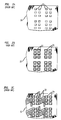
- Figs 2A to 2C show a prior art method for forming devices.
- Figs 3A to 3D show an alternative green tape method for forming devices.
- Figs. 1A-1D An embodiment of the process of the invention is shown in Figs. 1A-1D.
- Several green tape layers of a magnetic material are provided. It is possible to use a single layer, but greater than two layers are typically used.
- the magnetic material is selected from any magnetic material capable of being metallized, e.g., magnetic ceramics and polymers loaded with magnetic particles, and typically has a magnetic permability of about 400 to about 10000, and an electrical resistivity greater than about 10 6 ohm-cm.
- Green tape indicates a flexible material containing an organic binder and particles of the magnetic material. Typically, the tape contains about 8 to about 10 weight percent binder, based on the weight of the tape, with the remainder composed of a ceramic powder.
- the magnetic material is a spinel ferrite of the form M 1+x Fe 2-x 0 4-z , where x and z range from -0.1 to +0.1.
- M is typically at least one of manganese, magnesium, nickel, zinc, iron, copper, cobalt, vanadium, cadmium, and chromium.
- Advantageous ferrites are those exhibiting relatively high resistivities, e.g., about 10 4 ohm-cm or higher, such as nickel-zinc ferrites and certain manganese-zinc ferrites, which are also known as soft ferrites.
- Soft magnetic materials such as soft ferrites have coercivity less than about 10 Oe and are typically demagnetized in the absence of an external magnetic field.
- Other suitable ferrites include so-called microwave ferrites, e.g., the garnet structure, or so-called square-loop ferrites, e.g., where M is manganese or mangesium.
- Microwave ferrites are used for devices such as microwave circulators at frequencies in the range of 0.5 to 50 GHz.
- Square-loop ferrites exhibit a hysteresis loop with moderate coercivity and moderate remanence, and thus are capable of both regaining a flux density and being demagnetized in moderate magnetic fields.
- vias 12, 13 are punched into each green tape layer, at the same locations in each, and the layers are then stacked and laminated to form a multilayer substrate 10.
- Some of the vias 13 will be located along outer edges of the substrate (the left and right edges of the substrate shown in Fig. 1A). As mentioned previously, these vias 13 along the outer edges are referred to herein as outer vias, in contrast to the inner vias 12.
- These outer vias 13, due to their location along the edges of the substrate, are not intended to contact two opposing windings of devices. Typically, however, as reflected in Figs. 1C and 1D, an outer via 13 will contact both a winding 16 of a device and an opposing connection 15 to a bus 17.
- the bus distributes the needed current during electroplating. While rectangular vias are shown in the Figs. it is possible to form vias of a variety of geometries, e.g., square, circular, eliptical. Vias having aspect ratios (i.e., the ratio of the long to short axis) of about 1 to about 4 have been found to be useful. Vias 12, 13 are typically formed by placing the green tape layers in a suitable punch press. For green tapes formed from ceramic powder and organic binder, it is possible to laminate several layers of tape by pressing the layers together at a relatively low pressure, e.g., 250-3000 psi, at a temperature of about 50-100°C. To provide proper alignment of multiple layers, registration holes are typically punched in each layer during via formation, and registration rods are then placed through the holes to align the layers prior to lamination.
- a relatively low pressure e.g. 250-3000 psi
- the side walls of the vias 12, 13 are coated with a first conductive material 14, e.g., a conductive ink.
- a first conductive material 14 e.g., a conductive ink.
- the conductive material typically has a resistivity less than 10 -4 ohm-cm after firing).
- the coating step advantageously results in formation of continuous side walls. (A few discontinuities, e.g. pinholes, are acceptable as long as the post-fired conductive material is capable of being electroplated.)
- Useful conductive inks include those containing silver and/or palladium particles, or silver-palladium alloy particles (the silver and palladium generally used in a 70Ag:30Pd weight ratio).
- conductive inks typically contain the metal as a particular suspension in an organic binder, such that the ink is capable of being coated or screen printed.
- the first conductive material 14 is normally drawn through the vias using vacuum suction, optionally using a coating mask cut to match the via pattern in substrate 10. Other coating or deposition methods are also possible.
- the top and bottom surfaces of the substrate 10 are coated with a second conductive material 16, having post-fired properties similar to the first conductive material 14.
- the second conductive material 16 is screen printed to form a desired metallization pattern e.g., windings, circuit lines, and surface mount pads.
- the pattern formed from the second conductive material 16 contacts the material 14 coated onto the side walls of the vias 12, 13, thereby forming continuous, conductive windings.
- no expansion of the dimensions of the vias are needed, e.g., the vias 12, as initially punched, are capable of contacting two opposing windings.
- no expansion of the dimensions of the vias means that no affirmative expansion is performed, e.g., by further punching steps. Expansion of the vias due to other process steps, e.g., heat expansion during firing, is contemplated.) It is also possible to provide the surface coating of conductive material prior to lamination, and/or prior to via side wall coating. A bus 17 is also formed, along with contacts 15 from the bus 17 to the first conductive material 14 deposited in the outer vias 13.
- the second conductive material 16 is advantageously a conductive ink similar to the first conductive material 14 used to coat the inner side walls of the vias 12.
- the first conductive material 14 and the second conductive material 16 are silver-and palladium-containing ink that contains ferrite particles and an organic binder, advantageously a cellulose-based binder, this conductive ink discussed in detail below.
- the ink contains the same type ferrite as the substrate to improve adhesion to the substrate upon firing.
- the ink is typically screen printed to a wet thickness of 25 to 75 ⁇ m.
- scribe dice lines 18 into the green tape 10, as shown in Fig. 1D it is advantageous to scribe dice lines 18 into the green tape 10, as shown in Fig. 1D, to facilitate separation of devices subsequent to sintering of the article. It is also possible to omit the dice lines, and instead saw the devices apart after sintering is complete.
- the substrate 10 is fired. Firing drives solvent and binder from the first and second conductive material 14, 16, thereby adhering the metal particles to the substrate 10, and the firing also sinters the substrate 10 to a dense ceramic. Copper is then electroplated onto the fired conductive material 14, 16, generally to a thickness of about 1 to about 10 mils, to form the final devices.
- the bus 17 and contacts 15 to the outer vias 13 provide the needed current during electroplating. It is possible to use a variety of conventional electroplating baths to deposit the copper onto the conductive material, and such baths are discussed generally in Metal Finishing Guidebook, Vol. 94, No. 1A, 1996. Other conductive plating materials are also possible. Electroless plating is possible, but is typically slower and incapable of adequately providing a plating of desired thickness.
- the first and second conductive materials discussed in the embodiment above are advantageously a conductive ink containing silver/palladium particles, ferrite particles, an organic binder, and a solvent, where the solvent primarily solvates the binder.
- Use of ferrite particles are advantageous for improving adhesion of subsequent electroplating deposits on the conductive material, and for reducing the amount of costly silver and palladium material that is required.
- the silver/palladium particles are typically used in a weight ratio of 60-80 Ag:40-20 Pd (typically 70 Ag:30 Pd), and have an average diameter of about ⁇ m.
- the improved ink advantageously contains about 10 to about 50 wt.% ferrite particles, more advantageously about 20 to about 40 wt.%, in the post-fired material (i.e., based on the weight of the ferrite and conductive particles). Less than 10 wt.% ferrite particles typically results in an undesirably small increase in adhesion strength and cost reduction, while greater than 50 wt.% ferrite particles typically results in undesirably high electrical resistivity, which interferes with subsequent electroplating.
- the ferrite particles typically have an average diameter of about 0.2 to about 2.0 ⁇ m, advantageously about 1.5 ⁇ m.
- the ink typically contains about 1 to 3 wt.% of the organic binder, and about 10 to about 40 wt.% of the solvent, based on the weight prior to firing. At lower amounts of binder and solvent, the viscosity of the ink is typically too high to use in the process described above, while at higher amounts, the viscosity is typically too low.
- the organic binder provides desired rheology and strength to the green structure.
- the binder is advantageously cellulose-based and more advantageously ethyl cellulose.
- a variety of solvents are useful, including ⁇ -terpineol and mineral spirits.
- the binder is dissolved in a first solvent until substantially wet by the solvent.
- Particles of the ferrite and the conductive material are separately mixed with a second solvent (which is the same or different than the first solvent), e.g., ethanol, and typically a small amount, e.g., less than 1 wt.%, of a dispersant material such as oleic acid or another fatty acid.
- a second solvent which is the same or different than the first solvent
- a second solvent which is the same or different than the first solvent
- typically a small amount, e.g., less than 1 wt.%, of a dispersant material such as oleic acid or another fatty acid.
- Viscosity of the ink is typically adjusted by altering the arnount of solvent and/or binder. It is possible to use a control sample to determine the appropriate amounts of the components to provide a desired result. Normally, a less viscous ink is desired when plating the side walls of vias, e.g., 5,000 to 50,000 cp, whereas a more viscous ink, e.g., 30,000 to 300,000 cp, is useful for screen printing onto a surface of a ferrite substrate.
- a copper pyrophosphate bath generally contains four components. Copper pyrophosphate is the source of copper and a complexing ion. Potassium pyrophosphate further provides a complexing ion, and an amount of free pyrophosphate required for plating. Potassium nitrate provides for good anode corrosion. And ammonia (typically introduced as ammonium hydroxide) provides morphology control of the plated deposit. Typically, conventional pH adjusting compounds are also used. A useful, commercially-available pH lowering compound is "Compound 4A" available from ATOTECH, and pyrophosphoric acid is similarly suitable. A useful pH raising compound is potassium hydroxide.
- an additive is included to provide leveled, bright deposits, such additives commercially known and available. One such additive is additive PY61H, available from ATOTECH. Typically, leveler/brighteners consist of materials having organic backbones with attached alkoxy and/or hydroxyl groups.
- the temperature of the bath is advantageously 50 to 55°C. Below 50°C, the quality of the deposit is reduced, and above 55°C, pyrophosphate undesirably begins rapid conversion to orthophosphate.
- the pH of the bath is advantageously 7.8 to 8.5, more advantageously 8.0 to 8.5. At pH values below 7.8, pyrophosphate undesirably begins rapid conversion to orthophosphate. At pH values above 8.5 the quality of the deposit is reduced.
- Anodes are advantageously oxygen-free copper.
- the ammonia is advantageously present in an amount ranging from 6 to 10mL per L of bath solution.
- the orthophosphate concentration is advantageously less than 60 g/L, above which the orthophosphate lowers the quality of the plated deposit.
- the ammonium nitrate is advantageously present at a concentration of 8 to 12 g/L. within which desirable plating efficiency is attained.
- the ratio of pyrophosphate to copper is advantageously 7.7 to 8.5.
- the copper concentration is advantageously 19.0 to 25.0 g/L.
- Plating is advantageously performed at a current density of 25 to 50 ASF (amperes per square foot). It is possible to use a control sample to determine the particular parameters that will provide a desired result.
- a useful, commercially available copper pyrophosphate bath is the UNICHROMETM bath made by ATOTECH.
- a binder solution was formed by dissolving ethyl cellulose in ⁇ -terpineol, at a cellulose-terpineol weight ratio of between 1:10 and 1:12. The mixture was allowed to stand until the ethyl cellulose was substantially wet. The mixture was then passed through a 3-roll mill to further mix and homogenize the solution.
- Silver and palladium particles (70:30 weight ratio) and ferrite particles (the metal particles having average diameters of about 1 ⁇ m) were mixed with ethanol, in an amount approximately half the total weight of the metal particles, and 0.5 wt.% oleic acid was then added. (The amount of each type of metal was determined based on the desired ferrite loading). The mixture was then ultrasonicated for about 5 minutes. After several hours of settling of the metal particle mixture about 60 wt.% solvent was extracted. The metal powder, however, was not allowed to dry.
- the amount of binder solution needed to provide about 1.8 wt.% ethyl cellulose, based on the weight of the total ink (metal, ferrite, binder, and solvent) was determined and that determined amount was added to the metal powder.
- the mixture was manually mixed and placed onto a slow roller mill for homogenization.
- the mixture was placed onto a 3-roll mill to evaporate the ethanol and obtain a desired viscosity. If necessary, additional ⁇ -terpineol was added to adjust the viscosity.
- the ink contained 74 ⁇ 2 wt.% metal powders and 1.8 ⁇ 0.1 wt.% ethyl cellulose, based on the weight of the overall ink composition.
- An array of four turn, three layer surface mountable inductors was prepared in the following manner. Three 5" x 5" x 0.29" green, nickel-zinc ferrite (approximately Ni 0.4 Zn 0.6 Fe 2 0 4 ) tape layers were provided. Each tape contained ferrite powder and about 8 to about 10 wt.% organic binder. Vias having dimensions of 0.30" x 0.35" were punched in each tape layer individually, such that two adjacent devices would share four vias. Registration holes were also punched in each layer to allow subsequent stacking of the layers.
- Planar conductor patterns for windings and surface mount pads of the inductors), plating buss interconnects, and reference marks for scoring between the devices (to promote later separation) were provided on the top surface of the first tape layer and the bottom surface of the third tape layer.
- the planar conductor patterns and buss interconnects were formed from a silver-and palladium-containing ink made according to Example 1, containing 35 wt.% ferrite particles and 2 wt.% ethyl cellulose binder, with ⁇ -terpineol included to provide a desired viscosity.
- the three tape layers were then stacked on a steel registration fixture and laminated together at a temperature of about 80 to about 90°C and a pressure of about 250 to about 500 psi. Lamination caused the binder of the three layers to soften and fuse, thereby forming a relatively strong monolithic array.
- the side walls of the vias were then coated with the same metal ink used for the surface metallization. The viscosity of the ink was reduced beyond that used for the above printing step by addition of ⁇ -terpineol. The side walls were coated by drawing the ink through the vias with vacuum, to leave a coating on the side walls. After the ink dried, the array was scored on its top and bottom surfaces (as reflected in Fig. 1D) to promote singulation of the inductors subsequent to sintering and electroplating.
- the array was placed on a flat Alundum® setter that was dusted with a sintered ferrite powder of the same composition (to prevent the substrate from sticking to the AlundumTM).
- the array was then heated from room temperature to 500°C over about 24 hours to volatilize the organic components of the tape and ink in a controlled manner.
- the temperature was further raised to about 1100°C over about 24 hours, including a four hour treatment at about 1100°C and cooling to room temperature. All heating was performed in a flowing air atmosphere (2.5 L/minute).
- Plating of the fired array was performed in a copper pyrophosphate bath similar to the bath of Example 3, at 25 ASF, to a thickness of 0.005".
- a set of 0.08 inch diameter dots was patterned onto a green ferrite tape, using conductive ink made according to the process of Example 1, having the ferrite loading discussed below.
- the tape was then fired in air at about 1100°C for 4 hours.
- Copper was electroplated onto the dots to a thickness of 125 ⁇ m.
- the electroplating was performed in a copper sulphate acid bath at 25 ASF and room temperature.
- the bath contained 58.9 g/L of CuSO 4 , 120.0 mL/L of H 2 SO 4 , 3.0 mL/L of ATOTECH Cupracid Brightener, 15 mL/L of ATOTECH Cupracid BL-CT Basic Leveler, and 0.14 mL/L of HCI.
- Plating was performed at 25 ASF and room temperature. Copper studs were then attached to the copper dots with epoxy, and the pull strength was measured in a conventional manner using a Sebastian pull test apparatus.
- a set of 0.08 inch dots was patterned onto a green ferrite tape, using conductive ink made according to the process of Example 1 with a ferrite loading of 25 wt.% based on the weight of the fired ink.
- the tape was then fired in air at 1115°C for 4 hours. Copper was plated onto the dots to a thickness of 125 ⁇ m. The plating was performed in a copper pyrophosphate bath under the following conditions:
- Copper studs were then attached to the copper dots with epoxy, and the pull strength was measured in a conventional manner using a Sebastian pull test apparatus.
Landscapes
- Engineering & Computer Science (AREA)
- Power Engineering (AREA)
- Chemical & Material Sciences (AREA)
- Manufacturing & Machinery (AREA)
- Organic Chemistry (AREA)
- Metallurgy (AREA)
- Materials Engineering (AREA)
- Electrochemistry (AREA)
- Chemical Kinetics & Catalysis (AREA)
- Parts Printed On Printed Circuit Boards (AREA)
- Coils Or Transformers For Communication (AREA)
- Chemically Coating (AREA)
- Manufacturing Cores, Coils, And Magnets (AREA)
- Production Of Multi-Layered Print Wiring Board (AREA)
- Printing Elements For Providing Electric Connections Between Printed Circuits (AREA)
Applications Claiming Priority (3)
| Application Number | Priority Date | Filing Date | Title |
|---|---|---|---|
| US09/021,500 US6007758A (en) | 1998-02-10 | 1998-02-10 | Process for forming device comprising metallized magnetic substrates |
| US21500 | 1998-02-10 | ||
| EP99300743A EP0936639B1 (fr) | 1998-02-10 | 1999-02-02 | Procédé de fabrication d un dispositif comprenant des supports magnétiques métallisés |
Related Parent Applications (1)
| Application Number | Title | Priority Date | Filing Date |
|---|---|---|---|
| EP99300743A Division EP0936639B1 (fr) | 1998-02-10 | 1999-02-02 | Procédé de fabrication d un dispositif comprenant des supports magnétiques métallisés |
Publications (2)
| Publication Number | Publication Date |
|---|---|
| EP1017068A2 true EP1017068A2 (fr) | 2000-07-05 |
| EP1017068A3 EP1017068A3 (fr) | 2000-07-12 |
Family
ID=21804593
Family Applications (2)
| Application Number | Title | Priority Date | Filing Date |
|---|---|---|---|
| EP00107371A Withdrawn EP1017068A3 (fr) | 1998-02-10 | 1999-02-02 | Procédé de fabrication d' un dispositif comprenant des supports magnétiques métallisés |
| EP99300743A Expired - Lifetime EP0936639B1 (fr) | 1998-02-10 | 1999-02-02 | Procédé de fabrication d un dispositif comprenant des supports magnétiques métallisés |
Family Applications After (1)
| Application Number | Title | Priority Date | Filing Date |
|---|---|---|---|
| EP99300743A Expired - Lifetime EP0936639B1 (fr) | 1998-02-10 | 1999-02-02 | Procédé de fabrication d un dispositif comprenant des supports magnétiques métallisés |
Country Status (4)
| Country | Link |
|---|---|
| US (2) | US6007758A (fr) |
| EP (2) | EP1017068A3 (fr) |
| JP (1) | JPH11312619A (fr) |
| DE (1) | DE69903480D1 (fr) |
Families Citing this family (18)
| Publication number | Priority date | Publication date | Assignee | Title |
|---|---|---|---|---|
| US6007758A (en) * | 1998-02-10 | 1999-12-28 | Lucent Technologies Inc. | Process for forming device comprising metallized magnetic substrates |
| US6768906B2 (en) * | 1999-09-13 | 2004-07-27 | Motorola, Inc. | System and technique for plane switchover in an aircraft based wireless communication system |
| US6674355B2 (en) | 2000-05-19 | 2004-01-06 | M-Flex Multi-Fineline Electronix, Inc. | Slot core transformers |
| JP3722275B2 (ja) * | 2000-06-15 | 2005-11-30 | Tdk株式会社 | 金属粒子含有組成物、導電ペースト及びその製造方法 |
| AU2001294646A1 (en) * | 2000-09-22 | 2002-04-02 | M-Flex Multi-Fineline Electronix, Inc. | Electronic transformer/inductor devices and methods for making same |
| JP4674397B2 (ja) * | 2000-11-09 | 2011-04-20 | パナソニック株式会社 | セラミック素体の製造方法 |
| US6827834B2 (en) * | 2002-03-12 | 2004-12-07 | Ronald Stewart | Non-cyanide copper plating process for zinc and zinc alloys |
| US7135952B2 (en) | 2002-09-16 | 2006-11-14 | Multi-Fineline Electronix, Inc. | Electronic transformer/inductor devices and methods for making same |
| JP4157468B2 (ja) * | 2003-12-12 | 2008-10-01 | 日立電線株式会社 | 配線基板 |
| US7436282B2 (en) | 2004-12-07 | 2008-10-14 | Multi-Fineline Electronix, Inc. | Miniature circuitry and inductive components and methods for manufacturing same |
| KR101165116B1 (ko) | 2004-12-07 | 2012-07-12 | 멀티-파인라인 일렉트로닉스, 인크. | 소형 회로와 유도 소자 및 그 생산 방법 |
| CA2619997C (fr) * | 2005-08-24 | 2013-08-13 | A.M. Ramp & Co. Gmbh | Processus de production d'articles possedant un revetement conducteur d'electricite |
| US7645941B2 (en) | 2006-05-02 | 2010-01-12 | Multi-Fineline Electronix, Inc. | Shielded flexible circuits and methods for manufacturing same |
| US7449987B2 (en) | 2006-07-06 | 2008-11-11 | Harris Corporation | Transformer and associated method of making |
| US7340825B2 (en) * | 2006-07-06 | 2008-03-11 | Harris Corporation | Method of making a transformer |
| CN104327759B (zh) * | 2014-11-19 | 2016-07-06 | 深圳市宝尔威精密机械有限公司 | 一种用于料带接驳的贴胶带及其加工方法 |
| CN111455438B (zh) * | 2020-03-11 | 2022-07-15 | 贵州振华群英电器有限公司(国营第八九一厂) | 一种继电器基座局部电镀夹具 |
| JP2024003627A (ja) * | 2022-06-27 | 2024-01-15 | 株式会社村田製作所 | コイル部品の製造方法及びコイル部品 |
Family Cites Families (31)
| Publication number | Priority date | Publication date | Assignee | Title |
|---|---|---|---|---|
| GB690461A (en) * | 1951-01-12 | 1953-04-22 | Carrier Engineering Co Ltd | Improvements in or relating to air conditioning units |
| US3629939A (en) * | 1969-02-10 | 1971-12-28 | Sanders Associates Inc | Multilayer core memory process |
| GB1288992A (fr) * | 1970-06-22 | 1972-09-13 | ||
| US3731005A (en) * | 1971-05-18 | 1973-05-01 | Metalized Ceramics Corp | Laminated coil |
| US3812442A (en) * | 1972-02-29 | 1974-05-21 | W Muckelroy | Ceramic inductor |
| JPS5889819A (ja) * | 1981-11-20 | 1983-05-28 | Matsushita Electric Ind Co Ltd | チツプ・インダクタの製造方法 |
| JPS6261305A (ja) * | 1985-09-11 | 1987-03-18 | Murata Mfg Co Ltd | 積層チツプコイル |
| JPH065656B2 (ja) * | 1988-02-19 | 1994-01-19 | 株式会社村田製作所 | セラミック積層体の製造方法 |
| US5001014A (en) * | 1988-05-23 | 1991-03-19 | General Electric Company | Ferrite body containing metallization |
| JP2520450B2 (ja) * | 1988-06-02 | 1996-07-31 | 信越化学工業株式会社 | 耐食性希土類磁石の製造方法 |
| US5051154A (en) * | 1988-08-23 | 1991-09-24 | Shipley Company Inc. | Additive for acid-copper electroplating baths to increase throwing power |
| JPH0777085B2 (ja) * | 1989-02-28 | 1995-08-16 | 株式会社村田製作所 | フェライトチップ部品 |
| DE69220519T2 (de) * | 1991-03-04 | 1998-02-19 | Toda Kogyo Corp | Verfahren zur Plattierung eines Verbundmagneten sowie Verbundmagnet mit einem Metallüberzug |
| US5349743A (en) * | 1991-05-02 | 1994-09-27 | At&T Bell Laboratories | Method of making a multilayer monolithic magnet component |
| JPH04350913A (ja) * | 1991-05-28 | 1992-12-04 | Tokin Corp | 積層型インダクタの製造方法 |
| US5300911A (en) * | 1991-07-10 | 1994-04-05 | International Business Machines Corporation | Monolithic magnetic device with printed circuit interconnections |
| US5239744A (en) * | 1992-01-09 | 1993-08-31 | At&T Bell Laboratories | Method for making multilayer magnetic components |
| US5389428A (en) * | 1992-12-08 | 1995-02-14 | At&T Corp. | Sintered ceramic components and method for making same |
| JP3362429B2 (ja) * | 1993-01-12 | 2003-01-07 | 株式会社村田製作所 | 導電ペースト及びフェライト素子 |
| JPH06267788A (ja) * | 1993-03-15 | 1994-09-22 | Murata Mfg Co Ltd | 複合部品 |
| US5851681A (en) * | 1993-03-15 | 1998-12-22 | Hitachi, Ltd. | Wiring structure with metal wiring layers and polyimide layers, and fabrication process of multilayer wiring board |
| JPH0777085A (ja) * | 1993-09-10 | 1995-03-20 | Kubota Corp | エンジンのガバナ制御装置 |
| US5619791A (en) * | 1994-06-30 | 1997-04-15 | Lucent Technologies Inc. | Method for fabricating highly conductive vias |
| TW265450B (en) * | 1994-06-30 | 1995-12-11 | At & T Corp | Devices using metallized magnetic substrates |
| US5618611A (en) * | 1994-06-30 | 1997-04-08 | Lucent Technologies Inc. | Metallization of ferrites through surface reduction |
| US5647966A (en) * | 1994-10-04 | 1997-07-15 | Matsushita Electric Industrial Co., Ltd. | Method for producing a conductive pattern and method for producing a greensheet lamination body including the same |
| JP3123363B2 (ja) * | 1994-10-04 | 2001-01-09 | 三菱電機株式会社 | 携帯無線機 |
| US5821846A (en) * | 1995-05-22 | 1998-10-13 | Steward, Inc. | High current ferrite electromagnetic interference suppressor and associated method |
| US5650199A (en) * | 1995-11-22 | 1997-07-22 | Aem, Inc. | Method of making a multilayer electronic component with inter-layer conductor connection utilizing a conductive via forming ink |
| US5779873A (en) * | 1995-12-29 | 1998-07-14 | Lucent Technologies Inc. | Electroplating of nickel on nickel ferrite devices |
| US6007758A (en) * | 1998-02-10 | 1999-12-28 | Lucent Technologies Inc. | Process for forming device comprising metallized magnetic substrates |
-
1998
- 1998-02-10 US US09/021,500 patent/US6007758A/en not_active Expired - Fee Related
-
1999
- 1999-02-02 EP EP00107371A patent/EP1017068A3/fr not_active Withdrawn
- 1999-02-02 DE DE69903480T patent/DE69903480D1/de not_active Expired - Lifetime
- 1999-02-02 EP EP99300743A patent/EP0936639B1/fr not_active Expired - Lifetime
- 1999-02-10 JP JP11032151A patent/JPH11312619A/ja active Pending
- 1999-08-05 US US09/369,105 patent/US6153078A/en not_active Expired - Lifetime
Also Published As
| Publication number | Publication date |
|---|---|
| EP0936639B1 (fr) | 2002-10-16 |
| EP1017068A3 (fr) | 2000-07-12 |
| EP0936639A2 (fr) | 1999-08-18 |
| US6153078A (en) | 2000-11-28 |
| DE69903480D1 (de) | 2002-11-21 |
| US6007758A (en) | 1999-12-28 |
| EP0936639A3 (fr) | 1999-09-29 |
| JPH11312619A (ja) | 1999-11-09 |
Similar Documents
| Publication | Publication Date | Title |
|---|---|---|
| US6007758A (en) | Process for forming device comprising metallized magnetic substrates | |
| EP0690461B1 (fr) | Méthode de fabrication de dispositifs munis de substrats magnétiques métallisés | |
| EP1150311A2 (fr) | Matériau magnétique composite et matériau diélectrique composite pour parties électroniques | |
| US7403091B2 (en) | Inductance component and manufacturing method thereof | |
| KR20180036314A (ko) | 파워 인덕터 | |
| KR101830329B1 (ko) | 파워 인덕터 | |
| CA2216457C (fr) | Poudre de nickel et methode d'obtention | |
| EP0690035B1 (fr) | Métallisation d'un ferrite comprenant réduction de la surface | |
| US20150014899A1 (en) | Method for manufacturing laminated coil component | |
| US6815045B2 (en) | Method for manufacturing a metal powder, a metal powder, an electroconductive paste using the same, and a multilayer ceramic electronic component using the same | |
| WO2018181957A1 (fr) | Matériau magnétique composite, substrat comprenant un matériau magnétique composite, et composant électronique haute fréquence le comprenant | |
| CN111512710B (zh) | 印刷线路板用基材和印刷线路板 | |
| DE10020457A1 (de) | Elektronisches Bauteil und Funkgerät das dieses verwendet | |
| JP3546001B2 (ja) | 電子部品 | |
| US10827624B2 (en) | Catalytic laminate with conductive traces formed during lamination | |
| JP2005159064A (ja) | セラミック電子部品、及びセラミック電子部品の製造方法 | |
| EP0834368A1 (fr) | Poudre de nickel et son procédé de préparation | |
| CN110035603B (zh) | 一种印制电路埋嵌电感的制备方法 | |
| JP2000182832A (ja) | フェライトインダクタ及びその製造方法 | |
| JP2004022798A (ja) | 積層型インピーダンス素子、及びその製造方法 | |
| US20220238265A1 (en) | Multilayer coil device and method of manufacturing the same | |
| JP3126795B2 (ja) | セラミック積層部品の製造法 | |
| JP2009088197A (ja) | セラミック基板の製造方法 | |
| Cao et al. | Lateral growth of coating on Co2Z ferrite during electroplating of multilayer chip inductors | |
| CN118019239A (zh) | 一种埋置铁氧体电感印制板的制作方法 |
Legal Events
| Date | Code | Title | Description |
|---|---|---|---|
| PUAI | Public reference made under article 153(3) epc to a published international application that has entered the european phase |
Free format text: ORIGINAL CODE: 0009012 |
|
| PUAL | Search report despatched |
Free format text: ORIGINAL CODE: 0009013 |
|
| 17P | Request for examination filed |
Effective date: 20000413 |
|
| AC | Divisional application: reference to earlier application |
Ref document number: 936639 Country of ref document: EP |
|
| AK | Designated contracting states |
Kind code of ref document: A2 Designated state(s): DE FR GB |
|
| AX | Request for extension of the european patent |
Free format text: AL;LT;LV;MK;RO;SI |
|
| AK | Designated contracting states |
Kind code of ref document: A3 Designated state(s): AT BE CH CY DE DK ES FI FR GB GR IE IT LI LU MC NL PT SE |
|
| AX | Request for extension of the european patent |
Free format text: AL;LT;LV;MK;RO;SI |
|
| RIC1 | Information provided on ipc code assigned before grant |
Free format text: 7H 01F 41/04 A, 7C 25D 3/00 B, 7H 01F 41/16 B |
|
| AKX | Designation fees paid |
Free format text: DE FR GB |
|
| STAA | Information on the status of an ep patent application or granted ep patent |
Free format text: STATUS: THE APPLICATION HAS BEEN WITHDRAWN |
|
| 18W | Application withdrawn |
Effective date: 20030109 |