EP1017118A2 - Organische elektrolumineszente Vorrichtung und Herstellungsverfahren - Google Patents
Organische elektrolumineszente Vorrichtung und Herstellungsverfahren Download PDFInfo
- Publication number
- EP1017118A2 EP1017118A2 EP99310577A EP99310577A EP1017118A2 EP 1017118 A2 EP1017118 A2 EP 1017118A2 EP 99310577 A EP99310577 A EP 99310577A EP 99310577 A EP99310577 A EP 99310577A EP 1017118 A2 EP1017118 A2 EP 1017118A2
- Authority
- EP
- European Patent Office
- Prior art keywords
- layer
- light emitting
- electron
- transporting layer
- emitting layer
- Prior art date
- Legal status (The legal status is an assumption and is not a legal conclusion. Google has not performed a legal analysis and makes no representation as to the accuracy of the status listed.)
- Withdrawn
Links
- 238000004519 manufacturing process Methods 0.000 title description 5
- 239000000463 material Substances 0.000 claims abstract description 179
- 238000002347 injection Methods 0.000 claims abstract description 156
- 239000007924 injection Substances 0.000 claims abstract description 156
- 230000000452 restraining effect Effects 0.000 claims abstract description 145
- 238000000034 method Methods 0.000 claims description 83
- 150000001875 compounds Chemical class 0.000 claims description 19
- -1 aromatic tertiary amine Chemical class 0.000 claims description 9
- 125000004093 cyano group Chemical group *C#N 0.000 claims description 3
- 239000010410 layer Substances 0.000 description 501
- 230000000052 comparative effect Effects 0.000 description 70
- 238000007740 vapor deposition Methods 0.000 description 68
- 239000010408 film Substances 0.000 description 64
- 239000000758 substrate Substances 0.000 description 47
- TVIVIEFSHFOWTE-UHFFFAOYSA-K tri(quinolin-8-yloxy)alumane Chemical compound [Al+3].C1=CN=C2C([O-])=CC=CC2=C1.C1=CN=C2C([O-])=CC=CC2=C1.C1=CN=C2C([O-])=CC=CC2=C1 TVIVIEFSHFOWTE-UHFFFAOYSA-K 0.000 description 47
- UFVXQDWNSAGPHN-UHFFFAOYSA-K bis[(2-methylquinolin-8-yl)oxy]-(4-phenylphenoxy)alumane Chemical compound [Al+3].C1=CC=C([O-])C2=NC(C)=CC=C21.C1=CC=C([O-])C2=NC(C)=CC=C21.C1=CC([O-])=CC=C1C1=CC=CC=C1 UFVXQDWNSAGPHN-UHFFFAOYSA-K 0.000 description 27
- PQXKHYXIUOZZFA-UHFFFAOYSA-M lithium fluoride Chemical compound [Li+].[F-] PQXKHYXIUOZZFA-UHFFFAOYSA-M 0.000 description 22
- NLZUEZXRPGMBCV-UHFFFAOYSA-N Butylhydroxytoluene Chemical compound CC1=CC(C(C)(C)C)=C(O)C(C(C)(C)C)=C1 NLZUEZXRPGMBCV-UHFFFAOYSA-N 0.000 description 21
- 238000005406 washing Methods 0.000 description 20
- 238000010276 construction Methods 0.000 description 19
- KFZMGEQAYNKOFK-UHFFFAOYSA-N Isopropanol Chemical compound CC(C)O KFZMGEQAYNKOFK-UHFFFAOYSA-N 0.000 description 15
- 239000002585 base Substances 0.000 description 15
- 229910010272 inorganic material Inorganic materials 0.000 description 14
- 238000004040 coloring Methods 0.000 description 13
- 239000011368 organic material Substances 0.000 description 12
- 239000002356 single layer Substances 0.000 description 12
- 238000004528 spin coating Methods 0.000 description 11
- 238000004544 sputter deposition Methods 0.000 description 11
- CSCPPACGZOOCGX-UHFFFAOYSA-N Acetone Chemical compound CC(C)=O CSCPPACGZOOCGX-UHFFFAOYSA-N 0.000 description 10
- 238000001035 drying Methods 0.000 description 10
- 238000010030 laminating Methods 0.000 description 10
- 230000008569 process Effects 0.000 description 10
- XLYOFNOQVPJJNP-UHFFFAOYSA-N water Substances O XLYOFNOQVPJJNP-UHFFFAOYSA-N 0.000 description 10
- 230000004888 barrier function Effects 0.000 description 9
- 238000005229 chemical vapour deposition Methods 0.000 description 9
- 238000005268 plasma chemical vapour deposition Methods 0.000 description 9
- XKHYPFFZHSGMBE-UHFFFAOYSA-N buta-1,3-diene-1,1,2,3,4,4-hexacarbonitrile Chemical compound N#CC(C#N)=C(C#N)C(C#N)=C(C#N)C#N XKHYPFFZHSGMBE-UHFFFAOYSA-N 0.000 description 8
- 239000011147 inorganic material Substances 0.000 description 8
- CSHWQDPOILHKBI-UHFFFAOYSA-N peryrene Natural products C1=CC(C2=CC=CC=3C2=C2C=CC=3)=C3C2=CC=CC3=C1 CSHWQDPOILHKBI-UHFFFAOYSA-N 0.000 description 8
- 229920000642 polymer Polymers 0.000 description 8
- 229910052782 aluminium Inorganic materials 0.000 description 7
- AMGQUBHHOARCQH-UHFFFAOYSA-N indium;oxotin Chemical compound [In].[Sn]=O AMGQUBHHOARCQH-UHFFFAOYSA-N 0.000 description 7
- 239000012044 organic layer Substances 0.000 description 7
- 238000005215 recombination Methods 0.000 description 7
- 230000006798 recombination Effects 0.000 description 7
- XAGFODPZIPBFFR-UHFFFAOYSA-N aluminium Chemical compound [Al] XAGFODPZIPBFFR-UHFFFAOYSA-N 0.000 description 6
- 150000002484 inorganic compounds Chemical class 0.000 description 6
- 238000005259 measurement Methods 0.000 description 6
- 238000010438 heat treatment Methods 0.000 description 5
- 238000002360 preparation method Methods 0.000 description 5
- 239000007983 Tris buffer Substances 0.000 description 4
- 239000000654 additive Substances 0.000 description 4
- 230000000996 additive effect Effects 0.000 description 4
- XCJYREBRNVKWGJ-UHFFFAOYSA-N copper(II) phthalocyanine Chemical compound [Cu+2].C12=CC=CC=C2C(N=C2[N-]C(C3=CC=CC=C32)=N2)=NC1=NC([C]1C=CC=CC1=1)=NC=1N=C1[C]3C=CC=CC3=C2[N-]1 XCJYREBRNVKWGJ-UHFFFAOYSA-N 0.000 description 4
- 125000002080 perylenyl group Chemical group C1(=CC=C2C=CC=C3C4=CC=CC5=CC=CC(C1=C23)=C45)* 0.000 description 4
- IXHWGNYCZPISET-UHFFFAOYSA-N 2-[4-(dicyanomethylidene)-2,3,5,6-tetrafluorocyclohexa-2,5-dien-1-ylidene]propanedinitrile Chemical compound FC1=C(F)C(=C(C#N)C#N)C(F)=C(F)C1=C(C#N)C#N IXHWGNYCZPISET-UHFFFAOYSA-N 0.000 description 3
- 229910021417 amorphous silicon Inorganic materials 0.000 description 3
- 230000000694 effects Effects 0.000 description 3
- 229910052751 metal Inorganic materials 0.000 description 3
- 239000002184 metal Substances 0.000 description 3
- 239000000243 solution Substances 0.000 description 3
- 230000002269 spontaneous effect Effects 0.000 description 3
- NLDYACGHTUPAQU-UHFFFAOYSA-N tetracyanoethylene Chemical compound N#CC(C#N)=C(C#N)C#N NLDYACGHTUPAQU-UHFFFAOYSA-N 0.000 description 3
- ODHXBMXNKOYIBV-UHFFFAOYSA-N triphenylamine Chemical compound C1=CC=CC=C1N(C=1C=CC=CC=1)C1=CC=CC=C1 ODHXBMXNKOYIBV-UHFFFAOYSA-N 0.000 description 3
- PFNQVRZLDWYSCW-UHFFFAOYSA-N (fluoren-9-ylideneamino) n-naphthalen-1-ylcarbamate Chemical compound C12=CC=CC=C2C2=CC=CC=C2C1=NOC(=O)NC1=CC=CC2=CC=CC=C12 PFNQVRZLDWYSCW-UHFFFAOYSA-N 0.000 description 2
- FKNIDKXOANSRCS-UHFFFAOYSA-N 2,3,4-trinitrofluoren-1-one Chemical compound C1=CC=C2C3=C([N+](=O)[O-])C([N+]([O-])=O)=C([N+]([O-])=O)C(=O)C3=CC2=C1 FKNIDKXOANSRCS-UHFFFAOYSA-N 0.000 description 2
- LWHDQPLUIFIFFT-UHFFFAOYSA-N 2,3,5,6-tetrabromocyclohexa-2,5-diene-1,4-dione Chemical compound BrC1=C(Br)C(=O)C(Br)=C(Br)C1=O LWHDQPLUIFIFFT-UHFFFAOYSA-N 0.000 description 2
- JWWQNDLIYXEFQL-UHFFFAOYSA-N 2,3-dinitrofluoren-1-one Chemical compound C1=CC=C2C3=CC([N+](=O)[O-])=C([N+]([O-])=O)C(=O)C3=CC2=C1 JWWQNDLIYXEFQL-UHFFFAOYSA-N 0.000 description 2
- HONWGFNQCPRRFM-UHFFFAOYSA-N 2-n-(3-methylphenyl)-1-n,1-n,2-n-triphenylbenzene-1,2-diamine Chemical compound CC1=CC=CC(N(C=2C=CC=CC=2)C=2C(=CC=CC=2)N(C=2C=CC=CC=2)C=2C=CC=CC=2)=C1 HONWGFNQCPRRFM-UHFFFAOYSA-N 0.000 description 2
- OGGKVJMNFFSDEV-UHFFFAOYSA-N 3-methyl-n-[4-[4-(n-(3-methylphenyl)anilino)phenyl]phenyl]-n-phenylaniline Chemical compound CC1=CC=CC(N(C=2C=CC=CC=2)C=2C=CC(=CC=2)C=2C=CC(=CC=2)N(C=2C=CC=CC=2)C=2C=C(C)C=CC=2)=C1 OGGKVJMNFFSDEV-UHFFFAOYSA-N 0.000 description 2
- 239000005725 8-Hydroxyquinoline Substances 0.000 description 2
- YMWUJEATGCHHMB-UHFFFAOYSA-N Dichloromethane Chemical compound ClCCl YMWUJEATGCHHMB-UHFFFAOYSA-N 0.000 description 2
- NRCMAYZCPIVABH-UHFFFAOYSA-N Quinacridone Chemical compound N1C2=CC=CC=C2C(=O)C2=C1C=C1C(=O)C3=CC=CC=C3NC1=C2 NRCMAYZCPIVABH-UHFFFAOYSA-N 0.000 description 2
- 239000005083 Zinc sulfide Substances 0.000 description 2
- MWPLVEDNUUSJAV-UHFFFAOYSA-N anthracene Chemical compound C1=CC=CC2=CC3=CC=CC=C3C=C21 MWPLVEDNUUSJAV-UHFFFAOYSA-N 0.000 description 2
- 125000003118 aryl group Chemical group 0.000 description 2
- 230000005684 electric field Effects 0.000 description 2
- 239000007772 electrode material Substances 0.000 description 2
- 239000011521 glass Substances 0.000 description 2
- 230000006872 improvement Effects 0.000 description 2
- 239000011777 magnesium Substances 0.000 description 2
- 229910044991 metal oxide Inorganic materials 0.000 description 2
- 150000004706 metal oxides Chemical class 0.000 description 2
- 150000002894 organic compounds Chemical class 0.000 description 2
- 229960003540 oxyquinoline Drugs 0.000 description 2
- FIZIRKROSLGMPL-UHFFFAOYSA-N phenoxazin-1-one Chemical compound C1=CC=C2N=C3C(=O)C=CC=C3OC2=C1 FIZIRKROSLGMPL-UHFFFAOYSA-N 0.000 description 2
- UOMHBFAJZRZNQD-UHFFFAOYSA-N phenoxazone Natural products C1=CC=C2OC3=CC(=O)C=CC3=NC2=C1 UOMHBFAJZRZNQD-UHFFFAOYSA-N 0.000 description 2
- XHXFXVLFKHQFAL-UHFFFAOYSA-N phosphoryl trichloride Chemical compound ClP(Cl)(Cl)=O XHXFXVLFKHQFAL-UHFFFAOYSA-N 0.000 description 2
- 239000002985 plastic film Substances 0.000 description 2
- 229920000553 poly(phenylenevinylene) Polymers 0.000 description 2
- 125000003367 polycyclic group Chemical group 0.000 description 2
- BBEAQIROQSPTKN-UHFFFAOYSA-N pyrene Chemical compound C1=CC=C2C=CC3=CC=CC4=CC=C1C2=C43 BBEAQIROQSPTKN-UHFFFAOYSA-N 0.000 description 2
- MCJGNVYPOGVAJF-UHFFFAOYSA-N quinolin-8-ol Chemical compound C1=CN=C2C(O)=CC=CC2=C1 MCJGNVYPOGVAJF-UHFFFAOYSA-N 0.000 description 2
- YYMBJDOZVAITBP-UHFFFAOYSA-N rubrene Chemical compound C1=CC=CC=C1C(C1=C(C=2C=CC=CC=2)C2=CC=CC=C2C(C=2C=CC=CC=2)=C11)=C(C=CC=C2)C2=C1C1=CC=CC=C1 YYMBJDOZVAITBP-UHFFFAOYSA-N 0.000 description 2
- 229910052709 silver Inorganic materials 0.000 description 2
- PCCVSPMFGIFTHU-UHFFFAOYSA-N tetracyanoquinodimethane Chemical compound N#CC(C#N)=C1C=CC(=C(C#N)C#N)C=C1 PCCVSPMFGIFTHU-UHFFFAOYSA-N 0.000 description 2
- XOLBLPGZBRYERU-UHFFFAOYSA-N tin dioxide Chemical compound O=[Sn]=O XOLBLPGZBRYERU-UHFFFAOYSA-N 0.000 description 2
- 229910052984 zinc sulfide Inorganic materials 0.000 description 2
- DRDVZXDWVBGGMH-UHFFFAOYSA-N zinc;sulfide Chemical compound [S-2].[Zn+2] DRDVZXDWVBGGMH-UHFFFAOYSA-N 0.000 description 2
- NAWXUBYGYWOOIX-SFHVURJKSA-N (2s)-2-[[4-[2-(2,4-diaminoquinazolin-6-yl)ethyl]benzoyl]amino]-4-methylidenepentanedioic acid Chemical compound C1=CC2=NC(N)=NC(N)=C2C=C1CCC1=CC=C(C(=O)N[C@@H](CC(=C)C(O)=O)C(O)=O)C=C1 NAWXUBYGYWOOIX-SFHVURJKSA-N 0.000 description 1
- KLCLIOISYBHYDZ-UHFFFAOYSA-N 1,4,4-triphenylbuta-1,3-dienylbenzene Chemical compound C=1C=CC=CC=1C(C=1C=CC=CC=1)=CC=C(C=1C=CC=CC=1)C1=CC=CC=C1 KLCLIOISYBHYDZ-UHFFFAOYSA-N 0.000 description 1
- UVHXEHGUEKARKZ-UHFFFAOYSA-N 1-ethenylanthracene Chemical class C1=CC=C2C=C3C(C=C)=CC=CC3=CC2=C1 UVHXEHGUEKARKZ-UHFFFAOYSA-N 0.000 description 1
- IYZMXHQDXZKNCY-UHFFFAOYSA-N 1-n,1-n-diphenyl-4-n,4-n-bis[4-(n-phenylanilino)phenyl]benzene-1,4-diamine Chemical compound C1=CC=CC=C1N(C=1C=CC(=CC=1)N(C=1C=CC(=CC=1)N(C=1C=CC=CC=1)C=1C=CC=CC=1)C=1C=CC(=CC=1)N(C=1C=CC=CC=1)C=1C=CC=CC=1)C1=CC=CC=C1 IYZMXHQDXZKNCY-UHFFFAOYSA-N 0.000 description 1
- FQNVFRPAQRVHKO-UHFFFAOYSA-N 1-n,4-n-bis(4-methylphenyl)-1-n,4-n-diphenylbenzene-1,4-diamine Chemical compound C1=CC(C)=CC=C1N(C=1C=CC(=CC=1)N(C=1C=CC=CC=1)C=1C=CC(C)=CC=1)C1=CC=CC=C1 FQNVFRPAQRVHKO-UHFFFAOYSA-N 0.000 description 1
- JKLYZOGJWVAIQS-UHFFFAOYSA-N 2,3,5,6-tetrafluorocyclohexa-2,5-diene-1,4-dione Chemical compound FC1=C(F)C(=O)C(F)=C(F)C1=O JKLYZOGJWVAIQS-UHFFFAOYSA-N 0.000 description 1
- 229910017048 AsF6 Inorganic materials 0.000 description 1
- FYYHWMGAXLPEAU-UHFFFAOYSA-N Magnesium Chemical compound [Mg] FYYHWMGAXLPEAU-UHFFFAOYSA-N 0.000 description 1
- 229910019213 POCl3 Inorganic materials 0.000 description 1
- BQCADISMDOOEFD-UHFFFAOYSA-N Silver Chemical compound [Ag] BQCADISMDOOEFD-UHFFFAOYSA-N 0.000 description 1
- XBDYBAVJXHJMNQ-UHFFFAOYSA-N Tetrahydroanthracene Natural products C1=CC=C2C=C(CCCC3)C3=CC2=C1 XBDYBAVJXHJMNQ-UHFFFAOYSA-N 0.000 description 1
- HCHKCACWOHOZIP-UHFFFAOYSA-N Zinc Chemical compound [Zn] HCHKCACWOHOZIP-UHFFFAOYSA-N 0.000 description 1
- JFBZPFYRPYOZCQ-UHFFFAOYSA-N [Li].[Al] Chemical compound [Li].[Al] JFBZPFYRPYOZCQ-UHFFFAOYSA-N 0.000 description 1
- 238000010521 absorption reaction Methods 0.000 description 1
- 229910052783 alkali metal Inorganic materials 0.000 description 1
- 150000001340 alkali metals Chemical class 0.000 description 1
- 229910052784 alkaline earth metal Inorganic materials 0.000 description 1
- 150000001342 alkaline earth metals Chemical class 0.000 description 1
- 229910045601 alloy Inorganic materials 0.000 description 1
- 239000000956 alloy Substances 0.000 description 1
- 150000001448 anilines Chemical class 0.000 description 1
- HFACYLZERDEVSX-UHFFFAOYSA-N benzidine Chemical class C1=CC(N)=CC=C1C1=CC=C(N)C=C1 HFACYLZERDEVSX-UHFFFAOYSA-N 0.000 description 1
- 229910052794 bromium Inorganic materials 0.000 description 1
- 239000000969 carrier Substances 0.000 description 1
- 229910052801 chlorine Inorganic materials 0.000 description 1
- 239000002131 composite material Substances 0.000 description 1
- 229910052802 copper Inorganic materials 0.000 description 1
- 239000010949 copper Substances 0.000 description 1
- GVEPBJHOBDJJJI-UHFFFAOYSA-N fluoranthrene Natural products C1=CC(C2=CC=CC=C22)=C3C2=CC=CC3=C1 GVEPBJHOBDJJJI-UHFFFAOYSA-N 0.000 description 1
- 229910052737 gold Inorganic materials 0.000 description 1
- RBTKNAXYKSUFRK-UHFFFAOYSA-N heliogen blue Chemical compound [Cu].[N-]1C2=C(C=CC=C3)C3=C1N=C([N-]1)C3=CC=CC=C3C1=NC([N-]1)=C(C=CC=C3)C3=C1N=C([N-]1)C3=CC=CC=C3C1=N2 RBTKNAXYKSUFRK-UHFFFAOYSA-N 0.000 description 1
- 229910052738 indium Inorganic materials 0.000 description 1
- 229910052740 iodine Inorganic materials 0.000 description 1
- 229910052741 iridium Inorganic materials 0.000 description 1
- 239000007788 liquid Substances 0.000 description 1
- 239000004973 liquid crystal related substance Substances 0.000 description 1
- 229910052749 magnesium Inorganic materials 0.000 description 1
- SJCKRGFTWFGHGZ-UHFFFAOYSA-N magnesium silver Chemical compound [Mg].[Ag] SJCKRGFTWFGHGZ-UHFFFAOYSA-N 0.000 description 1
- 230000007246 mechanism Effects 0.000 description 1
- 150000002739 metals Chemical class 0.000 description 1
- 238000012986 modification Methods 0.000 description 1
- 230000004048 modification Effects 0.000 description 1
- DCZNSJVFOQPSRV-UHFFFAOYSA-N n,n-diphenyl-4-[4-(n-phenylanilino)phenyl]aniline Chemical compound C1=CC=CC=C1N(C=1C=CC(=CC=1)C=1C=CC(=CC=1)N(C=1C=CC=CC=1)C=1C=CC=CC=1)C1=CC=CC=C1 DCZNSJVFOQPSRV-UHFFFAOYSA-N 0.000 description 1
- IBHBKWKFFTZAHE-UHFFFAOYSA-N n-[4-[4-(n-naphthalen-1-ylanilino)phenyl]phenyl]-n-phenylnaphthalen-1-amine Chemical compound C1=CC=CC=C1N(C=1C2=CC=CC=C2C=CC=1)C1=CC=C(C=2C=CC(=CC=2)N(C=2C=CC=CC=2)C=2C3=CC=CC=C3C=CC=2)C=C1 IBHBKWKFFTZAHE-UHFFFAOYSA-N 0.000 description 1
- 125000000449 nitro group Chemical group [O-][N+](*)=O 0.000 description 1
- 150000002902 organometallic compounds Chemical class 0.000 description 1
- 150000004866 oxadiazoles Chemical class 0.000 description 1
- SLIUAWYAILUBJU-UHFFFAOYSA-N pentacene Chemical compound C1=CC=CC2=CC3=CC4=CC5=CC=CC=C5C=C4C=C3C=C21 SLIUAWYAILUBJU-UHFFFAOYSA-N 0.000 description 1
- 150000004986 phenylenediamines Chemical class 0.000 description 1
- 229920006255 plastic film Polymers 0.000 description 1
- 229910052697 platinum Inorganic materials 0.000 description 1
- 229920003227 poly(N-vinyl carbazole) Polymers 0.000 description 1
- 229920003229 poly(methyl methacrylate) Polymers 0.000 description 1
- 229920000548 poly(silane) polymer Polymers 0.000 description 1
- 229920000515 polycarbonate Polymers 0.000 description 1
- 239000004417 polycarbonate Substances 0.000 description 1
- 229920000728 polyester Polymers 0.000 description 1
- 239000002861 polymer material Substances 0.000 description 1
- 239000004926 polymethyl methacrylate Substances 0.000 description 1
- 239000010453 quartz Substances 0.000 description 1
- 229910052761 rare earth metal Inorganic materials 0.000 description 1
- HBMJWWWQQXIZIP-UHFFFAOYSA-N silicon carbide Chemical compound [Si+]#[C-] HBMJWWWQQXIZIP-UHFFFAOYSA-N 0.000 description 1
- VYPSYNLAJGMNEJ-UHFFFAOYSA-N silicon dioxide Inorganic materials O=[Si]=O VYPSYNLAJGMNEJ-UHFFFAOYSA-N 0.000 description 1
- 239000004332 silver Substances 0.000 description 1
- 239000002904 solvent Substances 0.000 description 1
- 238000003892 spreading Methods 0.000 description 1
- 230000007480 spreading Effects 0.000 description 1
- PJANXHGTPQOBST-UHFFFAOYSA-N stilbene Chemical group C=1C=CC=CC=1C=CC1=CC=CC=C1 PJANXHGTPQOBST-UHFFFAOYSA-N 0.000 description 1
- 125000001424 substituent group Chemical group 0.000 description 1
- IFLREYGFSNHWGE-UHFFFAOYSA-N tetracene Chemical compound C1=CC=CC2=CC3=CC4=CC=CC=C4C=C3C=C21 IFLREYGFSNHWGE-UHFFFAOYSA-N 0.000 description 1
- UGNWTBMOAKPKBL-UHFFFAOYSA-N tetrachloro-1,4-benzoquinone Chemical compound ClC1=C(Cl)C(=O)C(Cl)=C(Cl)C1=O UGNWTBMOAKPKBL-UHFFFAOYSA-N 0.000 description 1
- 239000010409 thin film Substances 0.000 description 1
- 150000001651 triphenylamine derivatives Chemical class 0.000 description 1
- 125000006617 triphenylamine group Chemical class 0.000 description 1
- 229910052721 tungsten Inorganic materials 0.000 description 1
- 229910052725 zinc Inorganic materials 0.000 description 1
- 239000011701 zinc Substances 0.000 description 1
Images

Classifications
-
- H—ELECTRICITY
- H10—SEMICONDUCTOR DEVICES; ELECTRIC SOLID-STATE DEVICES NOT OTHERWISE PROVIDED FOR
- H10K—ORGANIC ELECTRIC SOLID-STATE DEVICES
- H10K50/00—Organic light-emitting devices
- H10K50/10—OLEDs or polymer light-emitting diodes [PLED]
- H10K50/14—Carrier transporting layers
- H10K50/15—Hole transporting layers
- H10K50/155—Hole transporting layers comprising dopants
-
- H—ELECTRICITY
- H10—SEMICONDUCTOR DEVICES; ELECTRIC SOLID-STATE DEVICES NOT OTHERWISE PROVIDED FOR
- H10K—ORGANIC ELECTRIC SOLID-STATE DEVICES
- H10K50/00—Organic light-emitting devices
- H10K50/10—OLEDs or polymer light-emitting diodes [PLED]
- H10K50/11—OLEDs or polymer light-emitting diodes [PLED] characterised by the electroluminescent [EL] layers
-
- H—ELECTRICITY
- H10—SEMICONDUCTOR DEVICES; ELECTRIC SOLID-STATE DEVICES NOT OTHERWISE PROVIDED FOR
- H10K—ORGANIC ELECTRIC SOLID-STATE DEVICES
- H10K50/00—Organic light-emitting devices
- H10K50/10—OLEDs or polymer light-emitting diodes [PLED]
- H10K50/14—Carrier transporting layers
- H10K50/16—Electron transporting layers
- H10K50/165—Electron transporting layers comprising dopants
-
- H—ELECTRICITY
- H10—SEMICONDUCTOR DEVICES; ELECTRIC SOLID-STATE DEVICES NOT OTHERWISE PROVIDED FOR
- H10K—ORGANIC ELECTRIC SOLID-STATE DEVICES
- H10K50/00—Organic light-emitting devices
- H10K50/10—OLEDs or polymer light-emitting diodes [PLED]
- H10K50/18—Carrier blocking layers
-
- H—ELECTRICITY
- H10—SEMICONDUCTOR DEVICES; ELECTRIC SOLID-STATE DEVICES NOT OTHERWISE PROVIDED FOR
- H10K—ORGANIC ELECTRIC SOLID-STATE DEVICES
- H10K50/00—Organic light-emitting devices
- H10K50/10—OLEDs or polymer light-emitting diodes [PLED]
- H10K50/18—Carrier blocking layers
- H10K50/181—Electron blocking layers
-
- H—ELECTRICITY
- H10—SEMICONDUCTOR DEVICES; ELECTRIC SOLID-STATE DEVICES NOT OTHERWISE PROVIDED FOR
- H10K—ORGANIC ELECTRIC SOLID-STATE DEVICES
- H10K85/00—Organic materials used in the body or electrodes of devices covered by this subclass
- H10K85/30—Coordination compounds
- H10K85/311—Phthalocyanine
-
- H—ELECTRICITY
- H10—SEMICONDUCTOR DEVICES; ELECTRIC SOLID-STATE DEVICES NOT OTHERWISE PROVIDED FOR
- H10K—ORGANIC ELECTRIC SOLID-STATE DEVICES
- H10K85/00—Organic materials used in the body or electrodes of devices covered by this subclass
- H10K85/30—Coordination compounds
- H10K85/321—Metal complexes comprising a group IIIA element, e.g. Tris (8-hydroxyquinoline) gallium [Gaq3]
- H10K85/324—Metal complexes comprising a group IIIA element, e.g. Tris (8-hydroxyquinoline) gallium [Gaq3] comprising aluminium, e.g. Alq3
-
- H—ELECTRICITY
- H10—SEMICONDUCTOR DEVICES; ELECTRIC SOLID-STATE DEVICES NOT OTHERWISE PROVIDED FOR
- H10K—ORGANIC ELECTRIC SOLID-STATE DEVICES
- H10K85/00—Organic materials used in the body or electrodes of devices covered by this subclass
- H10K85/60—Organic compounds having low molecular weight
- H10K85/611—Charge transfer complexes
-
- H—ELECTRICITY
- H10—SEMICONDUCTOR DEVICES; ELECTRIC SOLID-STATE DEVICES NOT OTHERWISE PROVIDED FOR
- H10K—ORGANIC ELECTRIC SOLID-STATE DEVICES
- H10K85/00—Organic materials used in the body or electrodes of devices covered by this subclass
- H10K85/60—Organic compounds having low molecular weight
- H10K85/631—Amine compounds having at least two aryl rest on at least one amine-nitrogen atom, e.g. triphenylamine
-
- Y—GENERAL TAGGING OF NEW TECHNOLOGICAL DEVELOPMENTS; GENERAL TAGGING OF CROSS-SECTIONAL TECHNOLOGIES SPANNING OVER SEVERAL SECTIONS OF THE IPC; TECHNICAL SUBJECTS COVERED BY FORMER USPC CROSS-REFERENCE ART COLLECTIONS [XRACs] AND DIGESTS
- Y10—TECHNICAL SUBJECTS COVERED BY FORMER USPC
- Y10S—TECHNICAL SUBJECTS COVERED BY FORMER USPC CROSS-REFERENCE ART COLLECTIONS [XRACs] AND DIGESTS
- Y10S428/00—Stock material or miscellaneous articles
- Y10S428/917—Electroluminescent
Definitions
- the present invention relates to an organic electroluminescent element (organic EL element) and a production method thereof. More specifically, the invention relates to an organic EL element used for a display, etc., and to a production method thereof.
- a non-spontaneous light-emitting type liquid crystal display (LCD), a spontaneous light-emitting type plasma display (PDP), an EL display, etc. are known.
- the EL display is classified into two types of (1) an intrinsic EL element exciting a material (light emitting material) constituting a light emitting layer by the local transfer of electrons or holes in the light emitting layer and emitting light by an alternating current electric field and (2) a charge-injection type EL element exciting a light emitting material by the injection of electrons and holes from an electrode and the recombination of them in a light emitting layer and emitting light by a direct current electric field, from the differences in the light-emitting exciting mechanisms and the constituting materials.
- an intrinsic EL element exciting a material (light emitting material) constituting a light emitting layer by the local transfer of electrons or holes in the light emitting layer and emitting light by an alternating current electric field
- a charge-injection type EL element exciting a light emitting material by the injection of electrons and holes from an electrode and the recombination of them in a light emitting layer and emitting light by a direct current electric field, from the differences in the light-emit
- a display using, particularly, the organic EL element is being watched with extreme interest because the display has the features that the display is a spontaneous light emitting type, a low electric power consumption can be realized, the light-emitting color is various, etc.
- the organic EL element of prior art shown in Fig. 13 has the construction that on a transparent substrate 1 such as a glass are successively laminated an anode 2 made of an electrode material having a large work function, such as indium-tin oxide (ITO), a hole transporting layer 3 containing a hole transporting material 13, a light emitting layer 52, an electron transporting layer 7 containing an electron transporting material 17, and a cathode 8 made of an electrode material having a small work function, such as Mg/Ag.
- ITO indium-tin oxide
- a voltage is applied between the electrodes 2 and 8 to inject electrons and holes in the light emitting layer 52, and by releasing the recombination energy of an electron-hole pair formed in the light emitting layer as a fluorescence or a phosphorescence, a light is emitted.
- a dry process such as a vacuum vapor-deposition method of forming film on a substrate by heat-sublimating organic materials constituting the organic EL element in vacuum and a wet process such as a Langmuir-Blodgett method (LB method) of spreading an organic material on a liquid surface as a thin film and transferring the film onto a substrate and a spin-coating method of preparing a solution by dissolving an organic material in a solvent and spin-coating the solution by dropping the solution onto a substrate, etc., are known.
- LB method Langmuir-Blodgett method
- a coloring material used for each of the organic layers (a hole transporting layer, a light emitting layer, and an electron transporting layer) in the organic El element has the absorption ends from a visible light region to a ultraviolet region, the band gap is 1.5 eV or higher and there scarcely exists a carrier in the inside of each organic layer at room temperature. Also, the mobility of the carrier moving in the coloring material is generally small.
- the electric resistances of the organic layers are very high.
- the high-resistance characteristics of the organic layers cause voltage lowering of the element and generation of a Joule's heat and further by the causes, there occurs a problem that the light emitting efficiency and the life are lowered.
- the organic EL element strongly suggests the possibility as a full color flat panel display element of the next generation but in the production of the practical element, there are problems which must be solved.
- the present invention has been made for solving the above-described problems and an object of this invention is to provide an organic electroluminescent element of the construction having lowered resistances of organic layers, having a high light emitting efficiency, and being excellent in electrooptical characteristics and also to provide a production method of the organic electroluminescent element.
- an organic electroluminescent element comprising at least a light emitting layer containing an organic light emitting material placed between an anode and a cathode, wherein the element has, between the anode and the light emitting layer, at least a hole transporting layer containing a hole transporting material and an acceptor, and an electron injection restraining layer restraining the injection of electrons from the light emitting layer into the hole transporting layer, from the anode side, and/or, between the light emitting layer and the cathode, at least an electron transporting layer containing an electron transporting material and a donor, and a hole injection restraining layer restraining the injection of holes from the light emitting layer into the electron transporting layer, from the cathode side.
- a method of producing the above-described organic electroluminescent element comprising forming each of the anode, the hole transporting layer, the electron injection restraining layer, the light emitting layer, the hole injection restraining layer, the electron transporting layer, and the cathode by a vacuum film-forming method.
- an organic EL element there are, for example, the following constructions.
- the electron injection restraining layer is formed between the hole transporting layer and the light emitting layer.
- the height of the energy barrier making a role of confining electron in the light emitting layer can be more increased than the case of directly contacting the hole transporting layer and the light emitting layer. Accordingly, electrons can be effectively confined in the light emitting layer and in spite of that an acceptor is doped in the hole transporting layer, a high light emitting efficiency can be obtained.
- the electron injection restraining layer between the hole transporting layer and the light emitting layer as in this invention, the restraint of the injection of electrons into the light emitting layer becomes possible, whereby the occurrence of a leak current can be restrained.
- the organic EL element having a low resistance and a high light emitting efficiency and being excellent in the rectification characteristics can be realized.
- the electron injection restraining layer a known hole transporting material can be used. More preferably, to more effectively confine electrons in the light emitting layer, it is preferred that the electron affinity Ea (EBL) of a material constituting the electron injection restraining layer, the electron affinity Ea (A) of an acceptor, and the electron affinity Ea (EM) of a material (organic light emitting material) constituting the light emitting layer meet the following relation formula (1)
- the material cost is more reduced, it is preferred to use the same material as the hole transporting material used for the hole transporting layer as the material of constituting the electron injection restraining layer.
- the thickness of the electron injection restraining layer is thinner than 30 nm. This is because, if the thickness is 30 nm or thicker, the electron injection restraining layer acts as a resistance, the improvement of the electric conductivity of the hole transporting layer side by doping the acceptor is not remarkably obtained.
- the thickness of the electron injection restraining layer is more preferably from 5 to 20 nm.
- the hole injection restraining layer is formed between the light emitting layer and the electron transporting layer.
- the hole injection restraining layer By the existence of the hole injection restraining layer, the height of the energy barrier making the role of confining the holes in the light emitting layer can be more increased than the case of directly contacting the electron transporting layer and the light emitting layer.
- the holes can be effectively confined in the light emitting layer and in spite of that a donor is doped in the electron transporting layer, a high light emitting efficiency can be obtained.
- the hole injection restraining layer between the light emitting layer and the electron transporting layer as in this invention, the restraint of the injection of holes into the light emitting layer become possible, whereby the occurrence of the leak current can be restrained.
- an organic electroluminescent element having a low resistance and a high light emitting efficiency and being excellent in the rectification characteristics can be realized.
- the hole injection restraining layer a known electron transporting material can be used. More preferably, for more effectively confining holes in the light emitting layer, it is preferred that the ionization potential Ip (HBL) of the material constituting the hole injection restraining layer, the ionization potential Ip (D) of the donor, and the ionization potential Ip (EM) of the light emitting material meet following relation formula (2)
- the material cost can be reduced, it is preferred to use the material same as the electron transporting material used for the electron transporting layer as the material constituting the hole injection restraining layer.
- the thickness of the hole injection restraining layer is preferably thinner than 30 nm. If the thickness is 30 nm or thicker, the hole injection restraining layer acts as a resistance, whereby the improvement of the electric conductivity of the electron transporting layer side by doping the donor does not become remarkable. In addition, the thickness of the hole injection restraining layer is more preferably from 5 to 20 nm.
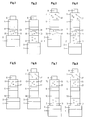
- the invention is explained by referring to Figs. 1 to 12.
- the above-described constitution (1) includes Fig. 1 and Fig. 2, the constitution (2) includes Fig. 3 and Fig. 4, the constitution (3) includes Fig. 5 and Fig. 6, the constitution (4) includes Fig. 7 and Fig. 8, and the constitution (5) includes Figs 9 to 12.
- Fig. 1 is a schematic cross-sectional view showing the organic EL element by the 1st embodiment of this invention.
- the organic EL element of Fig. 1 comprises an anode 2 formed on a transparent substrate 1, a hole transporting layer 31 containing at least a hole transporting material 13 and an acceptor 23, an electron injection restraining layer 4, a light emitting layer 5, and a cathode 8.
- each of the hole transporting layer 31, the electron injection restraining layer 4, and the light emitting layer 5 may be a single layer or multilayers.
- a substrate made of a plastic film or sheet of polyester, polymethyl methacrylate, polycarbonate, etc., a quartz sheet, a glass sheet, etc., can be used as the transparent substrate 1.
- a material having a large work function is preferably used as the material constituting the anode 2, from the view point of efficiently injecting holes in the hole transporting layer.
- a metal oxide such as indium tin oxide (ITO), SnO 2 , etc., and a metal such as Au, etc.
- ITO indium tin oxide
- SnO 2 SnO 2
- Au a metal such as Au
- the former (metal oxide) can be formed, for example, by a coating-burning method, and the latter (metal) can be formed by a sputtering method, a vacuum vapor-deposition method, etc.
- the hole transporting layer 31 contains at least the hole transporting material 13 and the acceptor 23 as described above.
- the hole transporting layer 31 may be constituted by the hole transporting material 13 and the acceptor 23 only or may further contain additive(s). Also, the hole transporting layer 31 may have a construction that the hole transporting material 13 and the acceptor 23 are dispersed in a high molecular compound or an inorganic compound.
- the hole transporting material 13 a known material can be used as the hole transporting material 13.
- Practical examples of the hole transporting material used in this invention include inorganic compounds such as p-type hydrogenated amorphous silicon, p-type hydrogenated amorphous silicon carbide, p-type zinc sulfide, p-type zinc selenide, etc.; aromatic amine-base compounds such as N,N'-bis-(3-methylphenyl)-N,N'-bis-(phenyl)-benzidine, N,N'-di(naphthylene-1-yl)-N,N'-bidiphenyl-benzidine), etc.; low-molecular materials such as hydrazone-base compounds, quinacridone-base compounds, phthalocyanine-base compounds, etc.; hole transporting polymers such as polyvinyl carbazole, etc.; ⁇ -conjugate system polymers such as poly-p-phenylenevinylene, etc.; and the organic compounds of ⁇
- the materials for the acceptor 23 include inorganic materials such as Au, Pt, W, Ir, POCl 3 , AsF 6 , Cl, Br, I, etc.; and organic materials, for example, compounds having a cyano group, such as TCNQ (7,7,8,8-tetracyanoquinodimethane), TCNQF 4 (tetrafluorotetracyanoquinodimethane), TCNE (tetracyanoethylene), HCNB (hexacyanobutadiene), DDQ (dicyclodicyanobenzoquinone), etc.; compounds having a nitro group, such as TNF (trinitrofluorenone), DNF (dinitrofluorenone), etc.; fluoranil, chloranil, bromanil, etc.
- the compounds having a cyano group such as TCNQ, TCNQF 4 , TCNE, HCNB, DDQ, etc., are more preferred.
- the addition ratio of the acceptor to the hole transporting material ( ⁇ (A) / ⁇ (HTM) ) is preferably from 1 to 20% by weight.
- the hole transporting layer 31 can be formed by a dry process such as a vacuum vapor deposition method, a CVD method, a plasma CVD method, a sputtering method, etc., or a wet process such as a spin coating method, an LB method, etc.
- the electron injection restraining layer 4 may be constituted by the hole transporting material 13 only but may have a construction that the hole transporting material 13 is dispersed in an inorganic material or an organic material such as a polymer.
- the electron injection restraining layer 4 can be formed by a dry process such as a vacuum vapor deposition method, a CVD method, a plasma CVD method, a sputtering method, etc., or a wet process such as a spin coating method, an LB method, etc.
- the light emitting layer 5 emits a light by the energy released by the recombination of holes moved from the anode 2 through the hole transporting layer 31 and the electron injection restraining layer 4 and electrons injected from the cathode 8.
- the light emitting layer 5 may be constituted by a light emitting material only or may have a construction that the light emitting material is dispersed in an inorganic material or an organic material such as a polymer.
- fluorescent organic materials such as aromatic dimethylidene compounds, oxadiazole compounds, etc.
- fluorescent organometallic compounds such as an azomethine zinc complex, the aluminum complex of 8-hydroxyquinoline, etc.
- polymers such as poly-p-phenylenevinylene, etc.
- the light emitting material may be doped with coumarin-base coloring materials, pyridine-base coloring materials, Rhodamine-base coloring materials, acridine-base coloring materials, and fluorescent coloring materials such as phenoxazone, DCM (4-(dicyanomethylene)-2-(methyl)-6-(4-dimethylaminostyryl)-4-pyran), quinacridone, rubrene, etc.
- the light emitting layer 5 can be formed by a dry process such as a vacuum vapor deposition method, a CVD method, a plasma CVD method, a sputtering method, etc., or a wet process such as a spin coating method, an LB method, etc.
- the material constituting the cathode 8 from the view point of the injection of electrons into the light emitting layer, a material having a small work function is preferably used. Practically, metals such as aluminum, etc.; alloys such as magnesium-silver, lithium-aluminum, etc., and composite films of magnesium and silver, lithium fluoride and aluminum, etc., can be used.
- the cathode 8 can be formed by sputtering, a vacuum vapor deposition method, etc.
- Fig. 2 is a schematic cross-sectional view showing the organic EL element by the 2nd embodiment of this invention.
- the organic EL element of Fig. 2 comprises an anode 2 formed on a transparent substrate 1, a hole transporting layer 3 containing at least a hole transporting material 13, a hole transporting layer 31 containing at least a hole transporting material 13 and an acceptor 23, an electron injection restraining layer 4, a light emitting layer 5, and a cathode 8.
- each of the hole transporting layers 3 and 31, the electron injection restraining layer 4, and the light emitting layer 5 may be a single layer or multilayers.
- the same materials as in the 1st embodiment of this invention described above can be used.
- the hole transporting layer 3 contains at least the hole transporting material 13 as described above.
- the hole transporting layer 3 may be constituted by the hole transporting material only or may further contain additive(s). Also, the layer has a construction that the hole transporting material 13 is dispersed in a high molecular compound or an inorganic compound.
- the hole transporting material 13 contained in the hole transporting layer 3 can be used as the hole transporting material 13 contained in the hole transporting layer 3 as the hole transporting material 13 contained in the hole transporting layer 3, the hole transporting material 13 contained in the hole transporting layer 31 mentioned above in the 1st embodiment of this invention can be used.
- the hole transporting layer 3 can be formed by a dry process such as a vacuum vapor deposition method, a CVD method, a plasma CVD method, a sputtering method, etc., or a wet process such as a spin coating method, an LB method, etc.
- Fig. 3 is a schematic cross-sectional view showing the organic EL element by the 3rd embodiment of this invention.
- the organic EL element of Fig. 3 comprises an anode 2 formed on a transparent substrate 1, a hole transporting layer 31 containing at least a hole transporting material 13 and an acceptor 23, an electron injection restraining layer 4, a light emitting layer 5, an electron transporting layer 7 containing at least an electron transporting material 17, and a cathode 8.
- each of the hole transporting layer 31, the electron injection restraining layer 4, the light emitting layer 5, and the electron transporting layer 7 may be a single layer or multilayers.
- the same materials as in the 1st embodiment of this invention described above can be used.
- the electron transporting layer 7 contains at least the electron transporting material 17 as described above.
- the electron transporting layer 7 may be constituted by the electron transporting material 17 only or may further contain additive(s). Also the layer 7 may have a construction that the electron transporting material 17 is dispersed in a high molecular compound or an inorganic compound.
- the electron transporting material 17 known materials can be used. Practically, inorganic compounds such as n-type hydrogenated amorphous silicon, n-type zinc sulfide, n-type zinc selenide, etc.; metal complex compounds such as the aluminum complex of 8-hydroxyquinoline, etc.; and organic compounds such as triazole-base compounds, oxadiazole-base compounds, xylol-base compounds, etc., can be used.
- the electron transporting layer 7 can be formed by a dry process such as a vacuum vapor deposition method, a CVD method, a plasma CVD method, a sputtering method, etc., or a wet process such as a spin coating method, an LB method, etc.
- Fig. 4 is a schematic cross-sectional view showing the organic EL element by the 4th embodiment of this invention.
- the organic EL element of Fig. 4 comprises an anode 2 formed on a transparent substrate 1, a hole transporting layer 3 containing at least a hole transporting material 13, a hole transporting layer 31 containing at least a hole transporting material 13 and an acceptor 23, an electron injection restraining layer 4, a light emitting layer 5, an electron transporting layer 7 containing at least an electron transporting material 17, and a cathode 8.
- each of the hole transporting layers 3 and 31, the electron injection restraining layer 4, the light emitting layer 5, and the electron transporting layer 7 may be a single layer or multilayers.
- the same materials as in the 1st to 3rd embodiments of this invention described above can be used.
- Fig. 5 is a schematic cross-sectional view showing the organic EL element of the 5th embodiment of this invention.
- the organic EL element of Fig. 5 comprises an anode 2 formed on a transparent substrate 1, a light emitting layer 51, a hole injection restraining layer 6, an electron transporting layer 71 containing at least an electron transporting material 17 and a donor 27, and a cathode 8.
- each of the light emitting layer 51, the hole injection restraining layer 6, and the electron transporting layer 71 may be a single layer or multilayers.
- the materials constituting the transparent substrate 1, the anode 2, and the cathode 8 by the 5th embodiment of this invention the same materials as in the 1st embodiment of this invention described above can be used.
- the light emitting layer 51 emits a light by the energy released by the recombination of the holes injected from the anode 2 and the electrons moved from the cathode 8 through the electron transporting layer 7 and the hole injection restraining layer 6.
- the light emitting layer 51 may be constituted by the light emitting material only or may have a construction that the light emitting material is dispersed in an inorganic material or an organic material such as a polymer.
- the light emitting material known materials can be used. Practically, diphenylethylene derivatives, vinyl anthracene derivatives, triphenylamine derivatives, etc., can be used. Furthermore, if necessary, the light emitting material may be doped with coumarin-base coloring materials, pyridine-base coloring materials, Rhodamine-base coloring materials, acridine-base coloring materials, and fluorescent coloring materials such as phenoxazone, DCM, quinacridone, rubrene, etc.
- the light emitting layer 51 can be formed by a dry process such as a vacuum vapor deposition method, a CVD method, a plasma CVD method, a sputtering method, etc., or a wet process such as a spin coating method, an LB method, etc.
- the electron transporting material 17 shown in the above-described 3rd embodiment of this invention can be used.
- the hole injection restraining layer 6 may be constituted by the electron transporting material 17 only or may have a construction that the electron transporting material 17 is dispersed in an inorganic material or an organic material such as a polymer.
- the hole injection restraining layer 6 can be formed by a dry process such as a vacuum vapor deposition method, a CVD method, a plasma CVD method, a sputtering method, etc., or a wet process such as a spin coating method, an LB method, etc.
- the electron transporting layer 71 contains at least the electron transporting material 17 and the donor 27 as described above.
- the electron transporting layer 71 may be constructed by the electron transporting material 17 and the donor 27 only or may further contain additive(s).
- the electron transporting layer 71 may have a construction that the electron transporting material 17 and the donor 27 are dispersed in a high molecular compound or an inorganic compound.
- the electron transporting material 17 the materials shown in the above-described 3rd embodiment of this invention can be used.
- the donor 27 includes inorganic materials such as alkali metals, alkaline earth metals, rare earth elements, Al, Ag, Cu, In, etc.; compounds having aromatic tertiary amine as the skeleton, such as anilines, phenylenediamines, benzidines [e.g., N,N,N',N'-tetraphenylbenzidine, N,N'-bis-(3-methylphenyl)-N,N'-bis-(phenyl)-benzidine, and N,N'-di(naphthalene-1-yl)-N,N'-diphenyl-benzidine], triphenylamines [e.g., triphenylamine, 4,4',4"-tris(N,N-diphenyl-amino)-triphenylamine, 4,4',4"-tris(N-3-methylphenyl-N-phenyl-amino)-triphenylamine, and 4,4',4"-
- the addition ratio of the donor to the electron transporting material ( ⁇ (D) / ⁇ (ETM) ) is preferably from 1 to 20% by weight.
- the electron transporting layer 71 can be formed by a dry process such as a vacuum vapor deposition method, a CVD method, a plasma CVD method, a sputtering method, etc., or a wet process such as a spin coating method, an LB method, etc.
- Fig. 6 is a schematic cross-sectional view showing the organic EL element of the 6th embodiment of this invention.
- the organic EL element of Fig. 6 comprises an anode 2 formed on a transparent substrate 1, a light emitting layer 51, a hole injection restraining layer 6, an electron transporting layer 71 containing at least an electron transporting material 17 and a donor 27, an electron transporting layer 7 containing at least an electron transporting material 17, and a cathode 8.
- each of the light emitting layer 51, the hole injection restraining layer 6, and the electron transporting layers 7 and 71 may be a single layer or multilayers.
- the materials constituting the layers of the 6th embodiment the materials same as those in the 1st, 3rd, and 5th embodiments of this invention described above can be used.
- Fig. 7 is a schematic cross-sectional view showing the organic EL element of the 7th embodiment of this invention.
- the organic EL element of Fig. 7 comprises an anode 2 formed on a transparent substrate 1, a hole transporting layer 3 containing at least a hole transporting material 13, a light emitting layer 51, a hole injection restraining layer 6, an electron transporting layer 71 containing at least an electron transporting material 17 and a donor 27, and a cathode 8.
- each of the hole transporting layer 3, the light emitting layer 51, the hole injection restraining layer 6, and the electron transporting layer 71 may be a single layer or multilayers.
- the materials constituting the layers of the 7th embodiment the materials same as those in the 1st, 2nd, and 5th embodiments of this invention described above can be used.
- Fig. 8 is a schematic cross-sectional view showing the organic EL element of the 8th embodiment of this invention.
- the organic EL element of Fig. 8 comprises an anode 2 formed on a transparent substrate 1, a hole transporting layer 3 containing at least a hole transporting material 13, a light emitting layer 51, a hole injection restraining layer 6, an electron transporting layer 71 containing at least an electron transporting material 17 and a donor 27, an electron transporting layer 7 containing at least an electron transporting material 17, and a cathode 8.
- each of the hole transporting layer 3, the light emitting layer 51, the hole injection restraining layer 6, the electron transporting layer 71 and the electron transporting layer 7 may be a single layer or multilayers.
- the materials constituting the layers of the 8th embodiment the materials same as those in the 1st, 2nd, 3rd and 5th embodiments of this invention described above can be used.
- Fig. 9 is a schematic cross-sectional view showing the organic EL element of the 9th embodiment of this invention.
- the organic EL element of Fig. 9 comprises an anode 2 formed on a transparent substrate 1, a hole transporting layer 31 containing at least a hole transporting material 13 and an acceptor 23, an electron injection restraining layer 4, a light emitting layer 52, a hole injection restraining layer 6, an electron transporting layer 71 containing at least an electron transporting material 17 and a donor 27, and a cathode 8.
- each of the hole transporting layer 31, the electron injection restraining layer 4, the light emitting layer 52, the hole injection restraining layer 6, and the electron transporting layer 71 may be a single layer or multilayers.
- the materials constituting the hole transporting layer 31 the electron injection restraining layer 4, the hole injection restraining layer 6, and the electron transporting layer 71 of the 9th embodiment, the materials same as those on the 1st and 5th embodiments of this invention described above can be used.
- the light emitting layer 52 emits a light by the energy released by the recombination of the holes moved from the anode 2 through the hole transporting layer 31 and the electron injection restraining layer 4 and the electrons moved from the cathode 8 through the electron transporting layer 71 and the hole injection restraining layer 6.
- the light emitting layer 52 may be composed of the light emitting material only or may have a construction that the light emitting material is dispersed in an inorganic material or an organic material such as a polymer.
- the same light emitting materials as in the 1st and 5th embodiments described above can be used.
- the light emitting material may be doped with the fluorescent coloring materials as in the 1st and 5th embodiments described above.
- the light emitting layer 52 can be formed by a dry process such as a vacuum vapor deposition method, a CVD method, a plasma CVD method, a sputtering method, etc., or a wet process such as a spin coating method, an LB method, etc.
- a dry process such as a vacuum vapor deposition method, a CVD method, a plasma CVD method, a sputtering method, etc.
- a wet process such as a spin coating method, an LB method, etc.
- Fig. 10 is a schematic view showing the organic EL element of the 10th embodiment of this invention.
- the organic EL element of Fig. 10 comprises an anode 2 formed on a transparent substrate 1, a hole transporting layer 3 containing at least a hole transporting material 13, a hole transporting layer 31 containing at least a hole transporting material 13 and an acceptor 23, an electron injection restraining layer 4, a light emitting layer 52, a hole injection restraining layer 6, an electron transporting layer 71 containing at least an electron transporting material 17 and a donor 27, and a cathode 8.
- each of the hole transporting layer 3, the hole transporting layer 31, the electron injection restraining layer 4, the light emitting layer 52, the hole injection restraining layer 6, and the electron transporting layer 71 may be a single layer or multilayers.
- the materials constituting the layers of the 10th embodiment the materials same as those in the 1st, 2nd, 5th and 9th embodiments of this invention described above can be used.
- Fig. 11 is a schematic cross-sectional view showing the organic EL element of the 11th embodiment of this invention.
- the organic EL element of Fig. 11 comprises an anode 2 formed on a transparent substrate 1, a hole transporting layer 31 containing at least a hole transporting material 13 and an acceptor 32, an electron injection restraining layer 4, a light emitting layer 52, a hole injection restraining layer 6, an electron transporting layer 71 containing at least an electron transporting material 17 and a donor 27, an electron transporting layer 7 containing at least an electron transporting material 17, and a cathode 8.
- each of the hole transporting layer 31, the electron injection restraining layer 4, the light emitting layer 52, the hole injection restraining layer 6, the electron transporting layer 71, and the electron transporting layer 7 may be a single layer or multilayers.
- the materials constituting the layers of the 11th embodiment the materials same as those in the 1st, 3rd, 5th and 9th embodiments of this invention described above can be used.
- Fig. 12 is a schematic cross-sectional view showing the organic EL element of the 12th embodiment of this invention.
- the organic EL element of Fig. 12 comprises an anode 2 formed on a transparent substrate 1, a hole transporting layer 3 containing at least a hole transporting material 13, a hole transporting layer 31 containing at least a hole transporting material 13 and an acceptor 23, an electron injection restraining layer 4, a light emitting layer 52, a hole injection restraining layer 6, an electron transporting layer 71 containing at least an electron transporting material 17 and a donor 27, an electron transporting layer 7 containing at least an electron transporting material 17, and a cathode 8.
- each of the hole transporting layer 3, the hole transporting layer 31, the electron injection restraining layer 4, the light emitting layer 52, the hole injection restraining layer 6, the electron transporting layer 71, and the electron transporting layer 7 may be a single layer or multilayers.
- the materials constituting the layers of the 12th embodiment the materials same as those in the 1st, 2nd, 3rd, 5th and 9th embodiments of this invention described above can be used.
- the hole transporting layer having a lower hole transporting faculty or the electron transporting layer having a lower electron transporting faculty dominates the resistance as the element. Therefore, when the hole transporting faculty of the hole transporting layer is lower, the resistance as the element can be reduced by doping the hole transporting layer with the acceptor and when the electron transporting faculty of the electron transporting layer is lower, the resistance as the element can be reduced by doping the electron transporting layer with the donor. Particularly, it is better that both the hole transporting layer and the electron transporting layer are doped with the acceptor and the donor respectively. In this case, both effects of the element wherein the hole transporting layer is doped with the acceptor and the electron transporting layer is doped with the donor can be obtained.
- a transparent substrate having formed on the surface thereof an indium-tin oxide (ITO) layer having a surface resistance of 10 ⁇ / and an area of 50 mm square was used, the ITO layer was patterned into stripes of 2 mm in width, after washing it with water, the substrate was subjected to pure-water ultrasonic washing for 10 minutes, acetone ultrasonic washing for 10 minutes, and isopropyl alcohol vapor washing for 5 minutes, and dried at 100°C for one hour. Then, the substrate was fixed to a substrate holder in a resistance-heating vapor deposition apparatus and the apparatus was evacuated to a vacuum of 1 ⁇ 10 -4 Pa or lower. In addition, the patterned ITO layer is used as an anode.
- ITO indium-tin oxide
- NPD N,N'-di(naphthylene-1-yl)-N,N'-bidiphenyl-benzidine
- Alq 3 tris(8-hydroxyquinolinato) aluminum (hereinafter, is referred to as simply Alq 3 ) shown by following structural formula (2) was laminated on the hole transporting layer at a vapor deposition rate of 0.2 nm/second such that the film thickness became 50 nm.
- a cathode made of LiF-Al was formed by laminating LiF on the light emitting layer at a vapor deposition rate of 0.02 nm/second such that the film thickness became 1 nm and by laminating A1 on the LiF film at a vapor deposition rate of 0.6 nm/second such that the film thickness became 100 nm.
- each of NPD and 7,7,8,8-tetracyanoquinodimethane (hereinafter, is referred to as simply TCNQ) shown by following structural formula (3) was laminated at vapor deposition rates of 0.4 nm/second and 0.004 nm/second respectively such that the film thickness became 100 nm, an organic EL element was obtained.
- each of NPD and hexacyanobutadiene (hereinafter, is referred as simply HCNB) shown by following structural formula (4) was laminated at vapor deposition rates of 0.4 nm/second and 0.04 nm/second respectively such that the film thickness became 100 nm, an organic EL element was obtained.
- a transparent substrate having formed on the surface thereof an indium-tin oxide (ITO) layer having a surface resistance of 10 ⁇ / and an area of 50 mm square was used, the ITO film was patterned into stripes of 2 mm in width, after washing it with water, the substrate was subjected to pure-water ultrasonic washing for 10 minutes, acetone ultrasonic washing for 10 minutes, and isopropyl alcohol vapor washing for 5 minutes, and dried at 100°C for one hour. Then, the substrate was fixed to a substrate holder in a resistance-heating vapor deposition apparatus and the apparatus was evacuated to a vacuum of 1 ⁇ 10 -4 Pa or lower. In addition, the patterned ITO is used as an anode.
- ITO indium-tin oxide
- NPD hole transporting layer
- BAlq bis(2-methyl-8-quinolinolato) (p-phenylphenolato) aluminum (hereinafter, is referred to as simply BAlq) shown by following structural formula (5) was laminated on the hole transporting layer at a vapor deposition rate of 0.2 nm/second such that the film thickness became 20 nm.
- Alq 3 was laminated on the light emitting layer at a vapor deposition rate of 0.2 nm/second such that the film thickness became 30 nm.
- a cathode made of LiF-Al was formed by laminating LiF on the light emitting layer at a vapor deposition rate of 0.02 nm/second such that the film thickness became 1 nm and by laminating A1 on the LiF layer at a vapor deposition rate of 0.6 nm/second such that the film thickness became 100 nm.
- an organic EL element composed of the anode, the hole transporting layer, the light emitting layer, the electron transporting layer, and the cathode was obtained.
- Example 3 By following the same procedure as Example 3 except that the electron injection restraining layer was laminated such that the film thickness became 5 nm, an organic EL element was obtained.
- Example 3 By following the same procedure as Example 3 except that the electron injection restraining layer was laminated such that the film thickness became 20 nm, an organic EL element was obtained.
- Example 3 By following the same procedure as Example 3 except that the electron injection restraining layer was laminated such that the film thickness became 30 nm, an organic EL element was obtained.
- each of NPD and TCNQ was laminated at vapor deposition rates of 0.4 nm/second and 0.02 nm/second respectively such that the film thickness became 100 nm, an organic EL element was obtained.
- each of NPD and TCNQ was laminated at vapor deposition rates of 0.4 nm/second and 0.04 nm/second respectively such that the film thickness became 100 nm, an organic EL element was obtained.
- Example 3 By following the same procedure as Example 3 except that as a 2nd hole transporting layer, CuPc was laminated between ITO and NPD at vapor deposition rates of 0.2 nm/second such that the film thickness became 15 nm, an organic EL element was obtained.
- the ionization potential (Ip) (measurement instrument: AC-1, manufactured by Riken Keiki K.K.) and the band gap (Eg) (measurement instrument: U-3410 type self-supporting spectrophotometer, manufactured by Hitachi, Ltd.) were determined and the electron affinity (Ea) was calculated therefrom. From the electron affinity obtained, the height of the energy barrier making a role of confining electrons in the light emitting layer was calculated.
- Example 1 With Comparative Example 2 and comparing Example 2 with Comparative Example 3, it can be seen that by forming the electron injection restraining layer between the hole transporting layer and the light emitting layer, lowering of the light emission efficiency can be restrained while lowering the applying voltage in a definite electric current value.
- Example 3 Examples 9 to 11 and Example 12 with Comparative Example 5, it can be seen that by forming the electron injection restraining layer between the hole transporting layer and the light emitting layer, lowering of the light emission efficiency can be restrained while lowering the applying voltage in a definite electric current value.
- Example 4 by comparing Example 4 with other examples, it can be seen that when the conditions of
- a transparent substrate having formed on the surface thereof an indium-tin oxide (ITO) layer having a surface resistance of 10 ⁇ / and an area of 50 mm square was used, the ITO layer was patterned into stripes of 2 mm in width, after washing it with water, the substrate was subjected to pure-water ultrasonic washing for 10 minutes, acetone ultrasonic washing for 10 minutes, and isopropyl alcohol vapor washing for 5 minutes, and dried at 100°C for one hour. Then, the substrate was fixed to a substrate holder in a resistance-heating vapor deposition apparatus and the apparatus was evacuated to a vacuum of 1 ⁇ 10 -4 Pa or lower. In addition, the patterned ITO layer is used as an anode.
- ITO indium-tin oxide
- TPB 1,1,4,4-tetraphenyl-1,3-butadiene
- tBu-PBD 2-(4-t-butylphenyl)-5-(4-biphenylyl)-1,3,4-oxazole
- a cathode made of LiF-Al was formed by laminating LiF on the light emitting layer at a vapor deposition rate of 0.02 nm/second such that the film thickness became 1 nm and by laminating A1 on the LiF film at a vapor deposition rate of 0.6 nm/second such that the film thickness became 100 nm.
- each of tBu-PBD and triphenylamine (hereinafter, is referred to as simply TPA) shown by following structural formula (10) was laminated at vapor deposition rates of 0.4 nm/second and 0.004 nm/second respectively such that the film thickness became 50 nm, an organic EL element was obtained.
- a transparent substrate having formed on the surface thereof an indium-tin oxide (ITO) layer having a surface resistance of 10 ⁇ / and an area of 50 mm square was used, the ITO layer was patterned into stripes of 2 mm in width, after washing it with water, the substrate was subjected to pure-water ultrasonic washing for 10 minutes, acetone washing for 10 minutes, and isopropyl alcohol vapor washing for 5 minutes, and dried at 100°C for one hour. Then, the substrate was fixed to a substrate holder in a resistance-heating vapor deposition apparatus and the apparatus was evacuated to a vacuum of 1 ⁇ 10 -4 Pa or lower. In addition, the patterned ITO layer is used as an anode.
- ITO indium-tin oxide
- NPD hole transporting layer
- BAlq was laminated on the hole transporting layer at a vapor deposition rate of 0.2 nm/second such that the film thickness became 20 nm.
- Alq 3 was laminated on the light emitting layer at a vapor deposition rate of 0.2 nm/second such that the film thickness became 30 nm.
- a cathode made of LiF-Al was formed by laminating LiF on the light emitting layer at a vapor deposition rate of 0.02 nm/second such that the film thickness became 1 nm and by laminating Al on the LiF film at a vapor deposition rate of 0.6 nm/second such that the film thickness became 100 nm.
- an organic EL element composed of the anode, the hole transporting layer, the light emitting layer, the electron transporting layer, and the cathode was obtained.
- each of Alq 3 and N,N'-di-(4-methyl-phenyl)-N,N'-diphenyl-1,4-phenylenediamine (hereinafter, is referred to as simply MPPD) shown by following structural formula (12) was laminated at vapor deposition rates of 0.4 nm/second and 0.004 nm/second respectively such that the film thickness became 30 nm, an organic EL element was obtained.
- Example 15 By following the same procedure as Example 15 except that the hole injection restraining layer was laminated such that the thickness thereof became 5 nm, an organic EL element was obtained.
- Example 15 By following the same procedure as Example 15 except that the hole injection restraining layer was laminated such that the thickness thereof became 20 nm, an organic EL element was obtained.
- Example 15 By following the same procedure as Example 15 except that the hole injection restraining layer was laminated such that the thickness thereof became 30 nm, an organic EL element was obtained.
- each of Alq 3 and TPA was laminated at vapor deposition rates of 0.4 nm/second and 0.02 nm/second such that the film thickness became 30 nm an organic EL element was obtained.
- each of Alq 3 and TPA was laminated at vapor deposition rates of 0.4 nm/second and 0.04 nm/second such that the film thickness became 30 nm an organic EL element was obtained.
- each of Alq 3 and TPA was laminated at vapor deposition rates of 0.4 nm/second and 0.08 nm/second such that the film thickness became 30 nm an organic EL element was obtained.
- Example 13 With Comparative Example 7 and comparing Example 14 with Comparative Example 8, it can be seen that by forming the hole injection restraining layer between the light emitting layer and the electron transporting layer, lowering of the light emission efficiency can be restrained while lowering the applying voltage in a definite electric current value.
- Example 15 and Example 18 it can be seen that as the height of the energy barrier between the hole injection restraining layer and the light emitting layer is higher, holes can be more effectively confined, whereby the light emission efficiency becomes better.
- a transparent substrate having formed on the surface thereof an indium-tin oxide (ITO) layer having a surface resistance of 10 ⁇ / and an area of 50 mm square was used, the ITO layer was patterned into stripes of 2 mm in width, after washing it with water, the substrate was subjected to pure-water ultrasonic washing for 10 minutes, acetone ultrasonic washing for 10 minutes, and isopropyl alcohol vapor washing for 5 minutes, and dried at 100°C for one hour. Then, the substrate was fixed to a substrate holder in a resistance-heating vapor deposition apparatus and the apparatus was evacuated to a vacuum of 1 ⁇ 10 -4 Pa or lower. In addition, the patterned ITO layer is used as an anode.
- ITO indium-tin oxide
- each of NPD and TCNQ was laminated on the substrate at vapor deposition rates of 0.4 nm/second and 0.004 nm/second respectively such that the film thickness became 50 nm.
- BAlq was laminated on the hole transporting layer at a vapor deposition rate of 0.2 nm/second such that the film thickness became 20 nm.
- each of Alq 3 and TPA was laminated on the light emitting layer at vapor deposition rates of 0.4 nm/second and 0.004 nm/second respectively such that the film thickness became 30 nm.
- a cathode made of LiF-Al was formed by laminating LiF on the light emitting layer at a vapor deposition rate of 0.02 nm/second such that the film thickness became 1 nm and by laminating Al on the LiF film at a vapor deposition rate of 0.6 nm/second such that the film thickness became 100 nm.
- an organic EL element composed of the anode, the hole transporting layer, the light emitting layer, the electron transporting layer, and the cathode was obtained.
- each of NPD and HCNB was laminated at vapor deposition rates of 0.4 nm/second and 0.004 nm/second respectively such that the film thickness became 50 nm and as the electron transporting layer, each of Alq 3 and perylene was laminated at vapor deposition rates of 0.4 nm/second and 0.004 nm/second respectively such that the film thickness became 30 nm, an organic EL element was obtained.
- an organic EL element having excellent electric characteristics (low resistance and high light emission efficiency) and the excellent rectification characteristics (the leak current under a reverse bias is small) can be obtained.
- the embodiments of the invention described above relate to an organic EL element. In principle, however the invention can be applied to any charge-injection type EL element, and is not limited to an organic EL element.
Landscapes
- Physics & Mathematics (AREA)
- Optics & Photonics (AREA)
- Electroluminescent Light Sources (AREA)
- Led Devices (AREA)
Applications Claiming Priority (2)
| Application Number | Priority Date | Filing Date | Title |
|---|---|---|---|
| JP37386598A JP2000196140A (ja) | 1998-12-28 | 1998-12-28 | 有機エレクトロルミネッセンス素子とその製造法 |
| JP37386598 | 1998-12-28 |
Publications (2)
| Publication Number | Publication Date |
|---|---|
| EP1017118A2 true EP1017118A2 (de) | 2000-07-05 |
| EP1017118A3 EP1017118A3 (de) | 2002-07-24 |
Family
ID=18502894
Family Applications (1)
| Application Number | Title | Priority Date | Filing Date |
|---|---|---|---|
| EP99310577A Withdrawn EP1017118A3 (de) | 1998-12-28 | 1999-12-24 | Organische elektrolumineszente Vorrichtung und Herstellungsverfahren |
Country Status (3)
| Country | Link |
|---|---|
| US (1) | US6566807B1 (de) |
| EP (1) | EP1017118A3 (de) |
| JP (1) | JP2000196140A (de) |
Cited By (50)
| Publication number | Priority date | Publication date | Assignee | Title |
|---|---|---|---|---|
| WO2002041414A1 (de) * | 2000-11-20 | 2002-05-23 | Novaled Gmbh | Lichtemittierendes bauelement mit organischen schichten |
| WO2003012890A2 (de) | 2001-07-20 | 2003-02-13 | Novaled Gmbh | Lichtemittierendes bauelement mit organischen schichten |
| WO2003022007A1 (en) | 2001-08-29 | 2003-03-13 | The Trustees Of Princeton University | Organic light emitting devices having carrier blocking layers comprising metal complexes |
| US6555840B1 (en) * | 1999-02-16 | 2003-04-29 | Sharp Kabushiki Kaisha | Charge-transport structures |
| WO2003083958A3 (de) * | 2002-03-28 | 2004-04-29 | Novaled Gmbh | Transparentes, thermisch stabiles lichtemittierendes bauelement mit organischen schichten |
| WO2004057686A3 (de) * | 2002-12-20 | 2005-01-06 | Novaled Gmbh | Lichtemittierende anordnung |
| EP1109234A3 (de) * | 1999-12-13 | 2005-07-13 | Samsung SDI Co., Ltd. | Organische elektrolumineszente Vorrichtung |
| WO2005050753A3 (en) * | 2003-11-14 | 2005-07-28 | Eastman Kodak Co | Organic electroluminescent devices having stability-enhancing layers |
| WO2005096401A3 (en) * | 2004-03-30 | 2005-11-10 | Osram Opto Semiconductors Gmbh | Device structure to improve oled reliability |
| EP1298737A3 (de) * | 2001-09-28 | 2005-12-14 | Eastman Kodak Company | Organische Licht emittierende Diode mit einer Zwischenschicht zwischen der Löcher transportierenden Schicht und der Licht emittierenden Schicht |
| EP1220340A3 (de) * | 2000-12-28 | 2006-01-18 | Semiconductor Energy Laboratory Co., Ltd. | Lumineszierende Anordnung |
| EP1624504A2 (de) | 2004-08-02 | 2006-02-08 | LG. Philips LCD Co., Ltd. | OLEDs mit einer ein inorganisches Material enthaltender Anode-Abdeckschicht |
| EP1624503A2 (de) | 2004-08-02 | 2006-02-08 | LG. Philips LCD Co., Ltd. | OLEDs mit verbesserter Luminanzstabilität |
| EP1508903A3 (de) * | 2003-08-18 | 2006-02-15 | Novaled GmbH | Dotierte organische Halbleitermaterialien sowie Verfahren zu deren Herstellung |
| EP1524707A3 (de) * | 2003-10-17 | 2006-04-26 | Junji Kido | Organische elektrolumineszente Vorrichtung und Herstellungsverfahren |
| EP1469534A3 (de) * | 2003-04-16 | 2006-05-10 | Eastman Kodak Company | Verfahren zur Herstellung einer emittierenden Schicht mit verbesserter Stabilität in einer OLED-Vorrichtung von einem Donorelement |
| WO2006098885A1 (en) * | 2005-03-10 | 2006-09-21 | Eastman Kodak Company | Electroluminescent devices with mixed electron transport materials |
| EP1713136A1 (de) * | 2005-04-13 | 2006-10-18 | Novaled AG | Anordnung für eine organische Leuchtdiode vom pin-Typ und Verfahren zum Herstellen |
| EP1265298A3 (de) * | 2001-06-06 | 2006-10-18 | Eastman Kodak Company | Organische lichtemittierende Vorrichtung mit farblose Dotierstoff in einem Ladungslöcher- und/oder Elektronentransportschicht |
| US7141817B2 (en) | 2001-11-30 | 2006-11-28 | Semiconductor Energy Laboratory Co., Ltd. | Light emitting device |
| WO2006131565A1 (fr) * | 2005-06-10 | 2006-12-14 | Thomson Licensing | Diode organique electroluminescente ne comprenant au plus que deux couches de materiaux organiques differents |
| EP1298738A3 (de) * | 2001-09-28 | 2006-12-27 | Eastman Kodak Company | Organische Leuchtdiode mit hoher Lichtausbeute |
| US7166010B2 (en) | 2002-06-26 | 2007-01-23 | 3M Innovative Properties Company | Buffer layers for organic electroluminescent devices and methods of manufacture and use |
| US7193291B2 (en) | 2004-03-25 | 2007-03-20 | 3M Innovative Properties Company | Organic Schottky diode |
| US7326473B2 (en) | 1998-02-17 | 2008-02-05 | Junji Kido | Organic electroluminescent devices |
| US7399536B2 (en) * | 2003-02-03 | 2008-07-15 | Samsung Sdi Co., Ltd. | Organic electroluminescent device driven at low voltage |
| US7420203B2 (en) | 2001-12-05 | 2008-09-02 | Semiconductor Energy Laboratory Co., Ltd. | Organic semiconductor element |
| US7449832B2 (en) | 2003-04-02 | 2008-11-11 | Fuji Photo Film Co., Ltd. | Organic electroluminescence device and organic electroluminescence display |
| US7485377B2 (en) * | 2003-08-14 | 2009-02-03 | Lg Electronics Inc. | Organic EL device |
| US7521113B2 (en) | 2003-04-28 | 2009-04-21 | Zheng-Hong Lu | Light-emitting devices with fullerene layer |
| WO2010068330A1 (en) * | 2008-12-12 | 2010-06-17 | Universal Display Corporation | Improved oled stability via doped hole transport layer |
| US7771843B2 (en) | 2003-06-24 | 2010-08-10 | Samsung Mobile Display Co., Ltd. | Organic light-emitting device employing doped hole transporting layer and/or hole injecting layer |
| EP1575339A4 (de) * | 2002-12-19 | 2010-09-01 | Semiconductor Energy Lab | Organisches elektrolumineszenzbauelement, lichtemittierendevorrichtung mit organischem elektrolumineszenzbauelement und eine solchelichtemittierende vorrichtung verwendendes elektrisches gerät |
| US7964891B2 (en) | 2004-08-04 | 2011-06-21 | Semiconductor Energy Laboratory Co., Ltd. | Light-emitting element, display device, and electronic appliance |
| EP2259360A3 (de) * | 2001-08-29 | 2011-08-10 | The Trustees of Princeton University | Organische Leuchtdioden mit Blockierschichten aus Metallkomplexen |
| US8110984B2 (en) | 2006-02-27 | 2012-02-07 | Commissariat A L'energie Atomique | Organic light-emitting diode with transparent multilayer electrode |
| USRE43319E1 (en) | 2003-08-27 | 2012-04-24 | Novaled Ag | Light-emitting component and process for its preparation |
| US8183559B2 (en) | 2002-05-21 | 2012-05-22 | Semiconductor Energy Laboratory Co., Ltd. | Organic field effect transistor |
| US8487527B2 (en) | 2005-05-04 | 2013-07-16 | Lg Display Co., Ltd. | Organic light emitting devices |
| US8629429B2 (en) | 2003-08-25 | 2014-01-14 | Semiconductor Energy Laboratory Co., Ltd. | Electrode device for organic device and electronic device having the same |
| US8659008B2 (en) | 2005-07-08 | 2014-02-25 | Semiconductor Energy Laboratory Co., Ltd. | Composite material and light emitting element, light emitting device, and electronic device using the composite material |
| EP2178347A4 (de) * | 2007-07-12 | 2014-08-27 | Sumitomo Chemical Co | Verfahren zur herstellung eines organischen leuchtbauelements |
| US8895155B2 (en) | 2004-11-29 | 2014-11-25 | Thomson Licensing | Organic light-emitting diode having doped layers |
| EP2461390A4 (de) * | 2009-07-31 | 2015-06-10 | Udc Ireland Ltd | Organisches elektrolumineszenzelement |
| US9184394B2 (en) | 2008-06-27 | 2015-11-10 | Universal Display Corporation | Cross linkable ionic compounds |
| CN102655225B (zh) * | 2007-10-19 | 2015-11-18 | 株式会社半导体能源研究所 | 发光元件的制造方法 |
| US9209415B2 (en) | 2009-09-04 | 2015-12-08 | Semiconductor Energy Laboratory Co., Ltd. | Light-emitting element with multiple light-emitting layers having controlled carrier mobility and lighting device and electronic device using the same |
| US20170186981A1 (en) * | 2015-12-28 | 2017-06-29 | Samsung Display Co., Ltd. | Organic light-emitting device |
| US10367049B2 (en) | 2005-11-04 | 2019-07-30 | Interdigital Ce Patent Holdings | Electro-optical element integrating an organic electroluminescent diode and an organic transistor for modulating said diode |
| US12110274B2 (en) | 2007-12-03 | 2024-10-08 | Semiconductor Energy Laboratory Co., Ltd. | Carbazole derivative, and light-emitting element, light-emitting device, and electronic device using carbazole derivative |
Families Citing this family (205)
| Publication number | Priority date | Publication date | Assignee | Title |
|---|---|---|---|---|
| JP3885412B2 (ja) * | 1999-05-25 | 2007-02-21 | 松下電器産業株式会社 | 有機電界発光素子 |
| US6580213B2 (en) * | 2000-01-31 | 2003-06-17 | Semiconductor Energy Laboratory Co., Ltd. | Light-emitting device and method of manufacturing the same |
| KR20010104215A (ko) * | 2000-05-12 | 2001-11-24 | 야마자끼 순페이 | 발광장치 제작방법 |
| JP4578642B2 (ja) * | 2000-08-09 | 2010-11-10 | 富士フイルム株式会社 | 有機発光素子 |
| JP2002141173A (ja) * | 2000-08-22 | 2002-05-17 | Semiconductor Energy Lab Co Ltd | 発光装置 |
| JP4560927B2 (ja) * | 2000-09-22 | 2010-10-13 | 住友化学株式会社 | 有機エレクトロルミネッセンス素子 |
| TW545080B (en) * | 2000-12-28 | 2003-08-01 | Semiconductor Energy Lab | Light emitting device and method of manufacturing the same |
| US7586115B2 (en) * | 2000-12-28 | 2009-09-08 | Epir Technologies, Inc. | Light emission from semiconductor integrated circuits |
| TW518909B (en) * | 2001-01-17 | 2003-01-21 | Semiconductor Energy Lab | Luminescent device and method of manufacturing same |
| TW519770B (en) * | 2001-01-18 | 2003-02-01 | Semiconductor Energy Lab | Light emitting device and manufacturing method thereof |
| US20020139303A1 (en) * | 2001-02-01 | 2002-10-03 | Shunpei Yamazaki | Deposition apparatus and deposition method |
| SG118110A1 (en) | 2001-02-01 | 2006-01-27 | Semiconductor Energy Lab | Organic light emitting element and display device using the element |
| TW582121B (en) * | 2001-02-08 | 2004-04-01 | Semiconductor Energy Lab | Light emitting device |
| US20030010288A1 (en) * | 2001-02-08 | 2003-01-16 | Shunpei Yamazaki | Film formation apparatus and film formation method |
| US7432116B2 (en) * | 2001-02-21 | 2008-10-07 | Semiconductor Energy Laboratory Co., Ltd. | Method and apparatus for film deposition |
| SG118118A1 (en) * | 2001-02-22 | 2006-01-27 | Semiconductor Energy Lab | Organic light emitting device and display using the same |
| WO2002071813A1 (en) * | 2001-03-02 | 2002-09-12 | The Trustees Of Princeton University | Double doped-layer, phosphorescent organic light emitting devices |
| US7288887B2 (en) * | 2001-03-08 | 2007-10-30 | Lg.Philips Lcd Co. Ltd. | Devices with multiple organic-metal mixed layers |
| JP4584506B2 (ja) * | 2001-08-28 | 2010-11-24 | パナソニック電工株式会社 | 有機電界発光素子 |
| KR100596028B1 (ko) * | 2001-11-12 | 2006-07-03 | 네오뷰코오롱 주식회사 | 고효율 유기 전계발광 소자 |
| JP2003323988A (ja) * | 2002-02-28 | 2003-11-14 | Semiconductor Energy Lab Co Ltd | 発光装置及びそれを用いた電気器具 |
| US6809481B2 (en) * | 2002-02-28 | 2004-10-26 | Semiconductor Energy Laboratory Co., Ltd. | Light emitting device and electric device using the same |
| US20100026176A1 (en) | 2002-03-28 | 2010-02-04 | Jan Blochwitz-Nomith | Transparent, Thermally Stable Light-Emitting Component Having Organic Layers |
| US6830830B2 (en) * | 2002-04-18 | 2004-12-14 | Canon Kabushiki Kaisha | Semiconducting hole injection materials for organic light emitting devices |
| US6931132B2 (en) * | 2002-05-10 | 2005-08-16 | Harris Corporation | Secure wireless local or metropolitan area network and related methods |
| EP1541657B2 (de) | 2002-07-19 | 2014-03-05 | Idemitsu Kosan Co., Ltd. | Organische elektrolumineszenzvorrichtungen und organisches lumineszenzmedium |
| JP2004063363A (ja) * | 2002-07-31 | 2004-02-26 | Semiconductor Energy Lab Co Ltd | 電界発光素子用材料、およびそれを用いた電界発光素子 |
| JPWO2004028217A1 (ja) * | 2002-09-20 | 2006-01-19 | 出光興産株式会社 | 有機エレクトロルミネッセンス素子 |
| KR100757721B1 (ko) * | 2002-11-06 | 2007-09-11 | 가부시키가이샤 도요다 지도숏키 | 유기 전계 발광 소자 |
| US6891326B2 (en) * | 2002-11-15 | 2005-05-10 | Universal Display Corporation | Structure and method of fabricating organic devices |
| CN1826840B (zh) * | 2002-12-19 | 2010-06-23 | 株式会社半导体能源研究所 | 发光装置及其制造方法 |
| US7345417B2 (en) * | 2002-12-19 | 2008-03-18 | Semiconductor Energy Laboratory Co., Ltd. | Light emitting device |
| TWI316827B (en) * | 2003-02-27 | 2009-11-01 | Toyota Jidoshokki Kk | Organic electroluminescent device |
| JP2004296226A (ja) * | 2003-03-26 | 2004-10-21 | Tsuchiya Co Ltd | 有機エレクトロルミネッセンス素子及びその作製方法 |
| JP2006526274A (ja) * | 2003-04-23 | 2006-11-16 | ツェン−ホン ルー | 埋込み電荷注入電極を有する発光デバイス |
| US7092206B2 (en) * | 2003-06-25 | 2006-08-15 | Hitachi Global Storage Technologies Netherlands B.V. | Magnetic head with magnetic layers of differing widths and third pole with reduced thickness |
| KR101246247B1 (ko) * | 2003-08-29 | 2013-03-21 | 가부시키가이샤 한도오따이 에네루기 켄큐쇼 | 전계발광소자 및 그것을 구비한 발광장치 |
| US6881502B2 (en) * | 2003-09-24 | 2005-04-19 | Eastman Kodak Company | Blue organic electroluminescent devices having a non-hole-blocking layer |
| TWI252055B (en) * | 2003-10-03 | 2006-03-21 | Pioneer Corp | Organic electroluminescent device |
| JP4243237B2 (ja) * | 2003-11-10 | 2009-03-25 | 淳二 城戸 | 有機素子、有機el素子、有機太陽電池、及び、有機fet構造、並びに、有機素子の製造方法 |
| JP4300176B2 (ja) * | 2003-11-13 | 2009-07-22 | ローム株式会社 | 有機エレクトロルミネッセント素子 |
| US7935433B2 (en) | 2003-12-25 | 2011-05-03 | Fujifilm Corporation | Organic EL element, organic EL display apparatus, method for manufacturing organic EL element, and apparatus for manufacturing organic EL element |
| CN101673808B (zh) * | 2003-12-26 | 2012-05-23 | 株式会社半导体能源研究所 | 发光元件 |
| JP4906235B2 (ja) * | 2004-03-10 | 2012-03-28 | 富士フイルム株式会社 | 有機電界発光素子 |
| US7622200B2 (en) * | 2004-05-21 | 2009-11-24 | Semiconductor Energy Laboratory Co., Ltd. | Light emitting element |
| JP4823566B2 (ja) * | 2004-05-21 | 2011-11-24 | 株式会社半導体エネルギー研究所 | 発光素子、表示装置及びテレビ受像器 |
| KR100587304B1 (ko) * | 2004-06-03 | 2006-06-08 | 엘지전자 주식회사 | 유기 el 소자 및 그 제조 방법 |
| DE102004035965B4 (de) * | 2004-07-23 | 2007-07-26 | Novaled Ag | Top-emittierendes, elektrolumineszierendes Bauelement mit zumindest einer organischen Schicht |
| JP4684042B2 (ja) * | 2004-08-04 | 2011-05-18 | 株式会社半導体エネルギー研究所 | 発光素子、発光装置および電子機器 |
| US7540978B2 (en) | 2004-08-05 | 2009-06-02 | Novaled Ag | Use of an organic matrix material for producing an organic semiconductor material, organic semiconductor material and electronic component |
| US7477013B2 (en) * | 2004-08-12 | 2009-01-13 | E. I. Du Pont De Nemours And Company | Organic light emitting devices with distinct resistance regions |
| JP2008509565A (ja) | 2004-08-13 | 2008-03-27 | ノヴァレッド・アクチエンゲゼルシャフト | 発光成分用積層体 |
| JP4782791B2 (ja) * | 2004-09-22 | 2011-09-28 | ドーサン・コーポレーション | 三原色光を利用する白色有機電界発光素子 |
| US8008652B2 (en) * | 2004-09-24 | 2011-08-30 | Semiconductor Energy Laboratory Co., Ltd. | Light emitting device |
| US7737626B2 (en) | 2004-09-30 | 2010-06-15 | Semiconductor Energy Laboratory Co., Ltd. | Light emitting element |
| EP1643568A1 (de) * | 2004-10-04 | 2006-04-05 | Novaled GmbH | Verfahren zum Herstellen einer Schicht aus einem dotierten Halbleitermaterial und Vorrichtung |
| EP1648042B1 (de) | 2004-10-07 | 2007-05-02 | Novaled AG | Verfahren zur Dotierung von einem Halbleitermaterial mit Cäsium |
| EP1653529B1 (de) | 2004-10-11 | 2007-11-21 | Samsung SDI Co., Ltd. | Organische elektrolumineszierende Vorrichtung und deren Herstellungsmethode |
| WO2006049323A1 (en) * | 2004-11-05 | 2006-05-11 | Semiconductor Energy Laboratory Co., Ltd. | Light-emitting element and light emitting device using the same |
| DE502005002342D1 (de) * | 2005-03-15 | 2008-02-07 | Novaled Ag | Lichtemittierendes Bauelement |
| JP2006278419A (ja) * | 2005-03-28 | 2006-10-12 | Osaka Univ | 有機エレクトロルミネッセンス素子 |
| US20080260970A1 (en) * | 2005-03-28 | 2008-10-23 | Kenichi Nakayama | Organic Electroluminescence Device |
| WO2006109878A1 (en) | 2005-04-11 | 2006-10-19 | Semiconductor Energy Laboratory Co., Ltd. | Light-emitting element, light-emitting device, and vapor deposition apparatus |
| US8057916B2 (en) * | 2005-04-20 | 2011-11-15 | Global Oled Technology, Llc. | OLED device with improved performance |
| US20060240277A1 (en) * | 2005-04-20 | 2006-10-26 | Eastman Kodak Company | Tandem OLED device |
| JP4801495B2 (ja) * | 2005-04-28 | 2011-10-26 | 株式会社半導体エネルギー研究所 | 発光素子および発光装置 |
| US7777407B2 (en) | 2005-05-04 | 2010-08-17 | Lg Display Co., Ltd. | Organic light emitting devices comprising a doped triazine electron transport layer |
| JP4915544B2 (ja) * | 2005-05-11 | 2012-04-11 | パナソニック株式会社 | 有機エレクトロルミネッセンス素子 |
| US7750561B2 (en) | 2005-05-20 | 2010-07-06 | Lg Display Co., Ltd. | Stacked OLED structure |
| US7811679B2 (en) | 2005-05-20 | 2010-10-12 | Lg Display Co., Ltd. | Display devices with light absorbing metal nanoparticle layers |
| US7728517B2 (en) | 2005-05-20 | 2010-06-01 | Lg Display Co., Ltd. | Intermediate electrodes for stacked OLEDs |
| US7943244B2 (en) | 2005-05-20 | 2011-05-17 | Lg Display Co., Ltd. | Display device with metal-organic mixed layer anodes |
| US7795806B2 (en) | 2005-05-20 | 2010-09-14 | Lg Display Co., Ltd. | Reduced reflectance display devices containing a thin-layer metal-organic mixed layer (MOML) |
| DE502005009415D1 (de) * | 2005-05-27 | 2010-05-27 | Novaled Ag | Transparente organische Leuchtdiode |
| EP2045843B1 (de) * | 2005-06-01 | 2012-08-01 | Novaled AG | Lichtemittierendes Bauteil mit einer Elektrodenanordnung |
| EP1739765A1 (de) * | 2005-07-01 | 2007-01-03 | Novaled AG | Organische Leuchtdiode und Anordnung mit mehreren organischen Leuchtdioden |
| JP4954623B2 (ja) * | 2005-07-08 | 2012-06-20 | 株式会社半導体エネルギー研究所 | 発光装置 |
| JP5546088B2 (ja) * | 2005-08-01 | 2014-07-09 | コニカミノルタ株式会社 | 有機エレクトロルミネッセンス素子 |
| JP2007073500A (ja) * | 2005-08-11 | 2007-03-22 | Semiconductor Energy Lab Co Ltd | 発光素子、発光装置及び電子機器 |
| WO2007028733A1 (de) * | 2005-09-05 | 2007-03-15 | Siemens Aktiengesellschaft | Neue materialien zur verbesserung der lochinjektion in organischen elektronischen bauelementen und verwendung des materials |
| TW200721478A (en) * | 2005-10-14 | 2007-06-01 | Pioneer Corp | Light-emitting element and display apparatus using the same |
| US7645524B2 (en) * | 2005-10-19 | 2010-01-12 | Eastman Kodak Company | OLED device with improved high temperature operation |
| EP1947911B1 (de) | 2005-11-09 | 2017-06-21 | Konica Minolta Holdings, Inc. | Organische elektrolumineszenzanordnung, display und beleuchtungseinrichtung |
| JP4853010B2 (ja) * | 2005-12-15 | 2012-01-11 | コニカミノルタホールディングス株式会社 | 有機エレクトロルミネッセンス素子および有機エレクトロルミネッセンスディスプレイ |
| JP4673279B2 (ja) * | 2005-12-20 | 2011-04-20 | 三星モバイルディスプレイ株式會社 | 有機発光表示素子及びその製造方法 |
| EP1806795B1 (de) * | 2005-12-21 | 2008-07-09 | Novaled AG | Organisches Bauelement |
| EP1804309B1 (de) * | 2005-12-23 | 2008-07-23 | Novaled AG | Elektronische Vorrichtung mit einer Schichtenstruktur von organischen Schichten |
| EP1804308B1 (de) * | 2005-12-23 | 2012-04-04 | Novaled AG | Organische lichtemittierende Vorrichtung mit mehreren aufeinander gestapelten organischen elektrolumineszenten Einheiten |
| CN101346830A (zh) | 2005-12-27 | 2009-01-14 | 出光兴产株式会社 | 有机电致发光元件用材料及有机电致发光元件 |
| US7935434B2 (en) | 2006-01-05 | 2011-05-03 | Konica Minolta Holdings, Inc. | Organic electroluminescent device, display, and illuminating device |
| JPWO2007080801A1 (ja) | 2006-01-11 | 2009-06-11 | 出光興産株式会社 | 新規イミド誘導体、有機エレクトロルミネッセンス素子用材料及びそれを用いた有機エレクトロルミネッセンス素子 |
| EP1808909A1 (de) | 2006-01-11 | 2007-07-18 | Novaled AG | Elekrolumineszente Lichtemissionseinrichtung |
| JP2007208102A (ja) * | 2006-02-03 | 2007-08-16 | Konica Minolta Holdings Inc | 有機エレクトロルミネッセンス素子、表示装置及び照明装置 |
| US7968904B2 (en) | 2006-02-06 | 2011-06-28 | Fujifilm Corporation | Organic electroluminescence device |
| WO2007095061A2 (en) * | 2006-02-09 | 2007-08-23 | Qd Vision, Inc. | Device including semiconductor nanocrystals and a layer including a doped organic material and methods |
| EP1994580B1 (de) * | 2006-02-28 | 2012-05-02 | Commissariat à l'Énergie Atomique et aux Énergies Alternatives | Elektronische komponente mit p-dotiertem organischem halbleiter |
| US20070210705A1 (en) * | 2006-03-09 | 2007-09-13 | Hajime Yokoi | Organic electroluminescent element and manufacturing method of an organic electroluminescent element and a display |
| JP2007243044A (ja) * | 2006-03-10 | 2007-09-20 | Fuji Electric Holdings Co Ltd | 有機el素子の製造方法 |
| TWI376980B (en) | 2006-03-14 | 2012-11-11 | Lg Chemical Ltd | Organic light emitting diode having high efficiency and process for fabricating the same |
| WO2007108362A1 (ja) | 2006-03-17 | 2007-09-27 | Konica Minolta Holdings, Inc. | 有機エレクトロルミネッセンス素子、表示装置および照明装置 |
| KR20080105127A (ko) | 2006-03-30 | 2008-12-03 | 이데미쓰 고산 가부시키가이샤 | 유기 전계발광 소자용 재료 및 이것을 사용한 유기 전계발광 소자 |
| JP5463668B2 (ja) | 2006-03-30 | 2014-04-09 | コニカミノルタ株式会社 | 有機エレクトロルミネッセンス素子、照明装置及びディスプレイ装置 |
| WO2007119473A1 (ja) | 2006-03-30 | 2007-10-25 | Konica Minolta Holdings, Inc. | 有機エレクトロルミネッセンス素子、有機エレクトロルミネッセンス素子の製造方法、照明装置及びディスプレイ装置 |
| EP1848049B1 (de) * | 2006-04-19 | 2009-12-09 | Novaled AG | Lichtemittierendes Bauelement |
| WO2008035406A1 (fr) * | 2006-09-20 | 2008-03-27 | Pioneer Corporation | Dispositif optique |
| KR101288128B1 (ko) * | 2006-12-11 | 2013-07-18 | 삼성디스플레이 주식회사 | 금속 프탈로시아닌기를 포함하는 덴드리머 중합체, 그의제조 방법 및 이를 채용한 유기 전계 발광 소자 |
| JP5493357B2 (ja) | 2006-12-13 | 2014-05-14 | コニカミノルタ株式会社 | 有機エレクトロルミネッセンス素子、表示装置及び照明装置 |
| DE102006059509B4 (de) * | 2006-12-14 | 2012-05-03 | Novaled Ag | Organisches Leuchtbauelement |
| JP5249781B2 (ja) | 2006-12-15 | 2013-07-31 | 出光興産株式会社 | 有機エレクトロルミネッセンス素子用材料及び有機エレクトロルミネッセンス素子 |
| KR20080067877A (ko) * | 2007-01-17 | 2008-07-22 | 삼성전자주식회사 | 표시장치 |
| US20080187748A1 (en) * | 2007-02-07 | 2008-08-07 | Masayuki Mishima | Organic electroluminescence device |
| DE102007019260B4 (de) * | 2007-04-17 | 2020-01-16 | Novaled Gmbh | Nichtflüchtiges organisches Speicherelement |
| US8044390B2 (en) | 2007-05-25 | 2011-10-25 | Idemitsu Kosan Co., Ltd. | Material for organic electroluminescent device, organic electroluminescent device, and organic electroluminescent display |
| JP5274459B2 (ja) | 2007-07-11 | 2013-08-28 | 出光興産株式会社 | 有機エレクトロルミネッセンス素子用材料及び有機エレクトロルミネッセンス素子 |
| US8288013B2 (en) | 2007-07-18 | 2012-10-16 | Idemitsu Kosan Co., Ltd. | Material for organic electroluminescence device and organic electroluminescence device |
| JP2009076865A (ja) | 2007-08-29 | 2009-04-09 | Fujifilm Corp | 有機電界発光素子 |
| JP5530608B2 (ja) * | 2007-09-13 | 2014-06-25 | 株式会社半導体エネルギー研究所 | 発光素子および発光装置 |
| KR101548382B1 (ko) | 2007-09-14 | 2015-08-28 | 유디씨 아일랜드 리미티드 | 유기 전계 발광 소자 |
| US7982216B2 (en) | 2007-11-15 | 2011-07-19 | Fujifilm Corporation | Thin film field effect transistor with amorphous oxide active layer and display using the same |
| US8319214B2 (en) | 2007-11-15 | 2012-11-27 | Fujifilm Corporation | Thin film field effect transistor with amorphous oxide active layer and display using the same |
| US8896201B2 (en) | 2008-02-19 | 2014-11-25 | Samsung Display Co., Ltd. | Organic light emitting device |
| KR100922757B1 (ko) | 2008-02-19 | 2009-10-21 | 삼성모바일디스플레이주식회사 | 수명을 향상시킨 유기 발광 소자 |
| KR20090092051A (ko) | 2008-02-26 | 2009-08-31 | 삼성모바일디스플레이주식회사 | 유기전계발광소자 및 그의 제조방법 |
| JP5243972B2 (ja) | 2008-02-28 | 2013-07-24 | ユー・ディー・シー アイルランド リミテッド | 有機電界発光素子 |
| KR100898075B1 (ko) * | 2008-03-04 | 2009-05-18 | 삼성모바일디스플레이주식회사 | 유기 발광 소자 |
| JP4555358B2 (ja) | 2008-03-24 | 2010-09-29 | 富士フイルム株式会社 | 薄膜電界効果型トランジスタおよび表示装置 |
| JP4531836B2 (ja) | 2008-04-22 | 2010-08-25 | 富士フイルム株式会社 | 有機電界発光素子並びに新規な白金錯体化合物及びその配位子となり得る新規化合物 |
| EP2460866B1 (de) | 2008-05-13 | 2019-12-11 | Konica Minolta Holdings, Inc. | Organisches elektrolumineszentes Element, Anzeigevorrichtung und Beleuchtungsvorrichtung |
| JP5551344B2 (ja) * | 2008-05-23 | 2014-07-16 | ローム株式会社 | 有機el素子 |
| KR100975867B1 (ko) * | 2008-06-19 | 2010-08-13 | 삼성모바일디스플레이주식회사 | 유기 발광 표시장치 |
| JP5098871B2 (ja) * | 2008-07-24 | 2012-12-12 | セイコーエプソン株式会社 | 発光素子、表示装置および電子機器 |
| DE102008036062B4 (de) | 2008-08-04 | 2015-11-12 | Novaled Ag | Organischer Feldeffekt-Transistor |
| DE102008036063B4 (de) * | 2008-08-04 | 2017-08-31 | Novaled Gmbh | Organischer Feldeffekt-Transistor |
| KR101069520B1 (ko) * | 2008-10-01 | 2011-09-30 | 주식회사 엘지화학 | 유기발광소자 및 이의 제조방법 |
| KR20100054110A (ko) | 2008-11-13 | 2010-05-24 | 주식회사 엘지화학 | 저전압 구동 유기발광소자 및 이의 제조 방법 |
| JP2010153820A (ja) | 2008-11-21 | 2010-07-08 | Fujifilm Corp | 有機電界発光素子 |
| JP4852660B2 (ja) * | 2008-12-18 | 2012-01-11 | パナソニック株式会社 | 有機エレクトロルミネッセンス表示装置及びその製造方法 |
| EP2383815B1 (de) | 2009-01-28 | 2014-07-30 | Konica Minolta Holdings, Inc. | Organisches elektrolumineszenzelement, anzeigevorrichtung und beleuchtungsvorrichtung |
| JP2010182449A (ja) | 2009-02-03 | 2010-08-19 | Fujifilm Corp | 有機el表示装置 |
| US9617255B2 (en) | 2009-02-06 | 2017-04-11 | Konica Minolta, Inc. | Organic electroluminescent element, and illumination device and display device each comprising the element |
| JP2010186723A (ja) | 2009-02-13 | 2010-08-26 | Fujifilm Corp | 有機el装置及びその製造方法 |
| JP2010205650A (ja) | 2009-03-05 | 2010-09-16 | Fujifilm Corp | 有機el表示装置 |
| JP5624784B2 (ja) * | 2009-03-31 | 2014-11-12 | 株式会社半導体エネルギー研究所 | ヘテロ芳香環を有する誘導体、ヘテロ芳香環を有する誘導体を用いた発光素子、発光装置、照明装置、電子機器 |
| WO2011004639A1 (ja) | 2009-07-07 | 2011-01-13 | コニカミノルタホールディングス株式会社 | 有機エレクトロルミネッセンス素子、新規な化合物、照明装置及び表示装置 |
| JP4598136B1 (ja) | 2009-07-31 | 2010-12-15 | 富士フイルム株式会社 | 有機電界発光素子及びその製造方法 |
| WO2011027657A1 (en) * | 2009-09-07 | 2011-03-10 | Semiconductor Energy Laboratory Co., Ltd. | Light-emitting element, light-emitting device, lighting device, and electronic device |
| JP2011060549A (ja) | 2009-09-09 | 2011-03-24 | Fujifilm Corp | 有機el装置用光学部材及び有機el装置 |
| JP5657243B2 (ja) | 2009-09-14 | 2015-01-21 | ユー・ディー・シー アイルランド リミテッド | カラーフィルタ及び発光表示素子 |
| JP5473506B2 (ja) | 2009-09-14 | 2014-04-16 | ユー・ディー・シー アイルランド リミテッド | カラーフィルタ及び発光表示素子 |
| JP2011139044A (ja) | 2009-12-01 | 2011-07-14 | Semiconductor Energy Lab Co Ltd | 発光素子、発光装置、電子機器、および照明装置 |
| WO2011102249A1 (ja) * | 2010-02-17 | 2011-08-25 | コニカミノルタホールディングス株式会社 | 有機電子デバイスの製造方法および有機電子デバイス |
| JP5658478B2 (ja) * | 2010-04-23 | 2015-01-28 | ユー・ディー・シー アイルランド リミテッド | 有機電界発光素子、並びにm−キンクフェニル構造を有する電荷輸送材料及び化合物 |
| JP5783780B2 (ja) * | 2010-06-03 | 2015-09-24 | キヤノン株式会社 | 表示装置 |
| JP2010226145A (ja) * | 2010-06-30 | 2010-10-07 | Fujifilm Corp | 有機発光素子 |
| JP5761199B2 (ja) | 2010-10-22 | 2015-08-12 | コニカミノルタ株式会社 | 有機エレクトロルミネッセンス素子 |
| US9368735B2 (en) | 2011-02-15 | 2016-06-14 | Konica Minolta, Inc. | Organic electroluminescence element and illumination device |
| US9923154B2 (en) | 2011-02-16 | 2018-03-20 | Konica Minolta, Inc. | Organic electroluminescent element, lighting device, and display device |
| EP2696660A4 (de) | 2011-04-06 | 2014-10-22 | Konica Minolta Inc | Verfahren zur herstellung eines organischen elektrolumineszenzelements und organisches elektrolumineszenzelement |
| WO2012137640A1 (ja) | 2011-04-07 | 2012-10-11 | コニカミノルタホールディングス株式会社 | 有機エレクトロルミネッセンス素子及び照明装置 |
| WO2012153603A1 (ja) | 2011-05-10 | 2012-11-15 | コニカミノルタホールディングス株式会社 | 燐光発光有機エレクトロルミネッセンス素子及び照明装置 |
| EP2728639B1 (de) | 2011-06-28 | 2018-04-18 | Konica Minolta, Inc. | Organisches elektrolumineszenzelement und sein herstellungsverfahren |
| JP5928469B2 (ja) | 2011-08-09 | 2016-06-01 | コニカミノルタ株式会社 | 有機光電変換素子、およびそれを用いた有機太陽電池 |
| JP5742586B2 (ja) | 2011-08-25 | 2015-07-01 | コニカミノルタ株式会社 | 有機エレクトロルミネッセンス素子、照明装置及び表示装置 |
| JPWO2013031662A1 (ja) * | 2011-08-26 | 2015-03-23 | コニカミノルタ株式会社 | 有機エレクトロルミネッセンス素子、照明装置及び表示装置 |
| WO2013032303A2 (ko) * | 2011-09-02 | 2013-03-07 | 주식회사 엘엠에스 | 유기전자소자 |
| JPWO2013035490A1 (ja) | 2011-09-07 | 2015-03-23 | コニカミノルタ株式会社 | 有機エレクトロルミネッセンス素子、照明装置及び表示装置 |
| EP2760059A4 (de) | 2011-09-21 | 2015-08-05 | Konica Minolta Inc | Organisches elektrolumineszenzelement, anzeigevorrichtung und beleuchtungsvorrichtung |
| WO2013073302A1 (ja) | 2011-11-14 | 2013-05-23 | コニカミノルタ株式会社 | 有機エレクトロルミネッセンス素子、及び、面状発光体 |
| WO2013073301A1 (ja) | 2011-11-14 | 2013-05-23 | コニカミノルタ株式会社 | 有機エレクトロルミネッセンス素子、及び、面状発光体 |
| EP2781347B1 (de) | 2011-11-17 | 2019-11-20 | Konica Minolta, Inc. | Transparente elektrode und elektronische vorrichtung |
| WO2013099867A1 (ja) | 2011-12-27 | 2013-07-04 | コニカミノルタ株式会社 | 透明電極、電子デバイス、有機電界発光素子、および有機電界発光素子の製造方法 |
| JP5978843B2 (ja) | 2012-02-02 | 2016-08-24 | コニカミノルタ株式会社 | イリジウム錯体化合物、有機エレクトロルミネッセンス素子材料、有機エレクトロルミネッセンス素子、照明装置及び表示装置 |
| JP6137170B2 (ja) | 2012-03-21 | 2017-05-31 | コニカミノルタ株式会社 | 有機電界発光素子 |
| US9947889B2 (en) | 2012-04-23 | 2018-04-17 | Konica Minolta Inc. | Transparent electrode, electronic device, and organic electroluminescent element |
| WO2013161603A1 (ja) | 2012-04-24 | 2013-10-31 | コニカミノルタ株式会社 | 透明電極、電子デバイス、および透明電極の製造方法 |
| JP5880274B2 (ja) | 2012-05-21 | 2016-03-08 | コニカミノルタ株式会社 | 有機エレクトロルミネッセンス素子、照明装置及び表示装置 |
| JP5849867B2 (ja) | 2012-06-21 | 2016-02-03 | コニカミノルタ株式会社 | 有機エレクトロルミネッセンス素子、表示装置及び照明装置 |
| WO2014024668A1 (ja) | 2012-08-07 | 2014-02-13 | コニカミノルタ株式会社 | 有機エレクトロルミネッセンス素子、照明装置及び表示装置 |
| WO2014030666A1 (ja) | 2012-08-24 | 2014-02-27 | コニカミノルタ株式会社 | 透明電極、電子デバイス、および透明電極の製造方法 |
| WO2014038456A1 (ja) | 2012-09-04 | 2014-03-13 | コニカミノルタ株式会社 | 有機エレクトロルミネッセンス素子、照明装置及び表示装置 |
| KR101960468B1 (ko) * | 2012-10-08 | 2019-03-21 | 삼성전자주식회사 | 유기 광전 소자 및 이미지 센서 |
| CN104797644A (zh) * | 2012-12-03 | 2015-07-22 | 阿克伦大学 | 具有宽带响应和增加的光电响应度的有机聚合物光电装置 |
| EP2930762B1 (de) | 2012-12-10 | 2020-09-16 | Konica Minolta, Inc. | Material für ein organisches elektrolumineszenzelement, organisches elektrolumineszenzelement, beleuchtungsvorrichtung und anzeigevorrichtung |
| WO2014092014A1 (ja) | 2012-12-10 | 2014-06-19 | コニカミノルタ株式会社 | 有機エレクトロルミネッセンス素子、照明装置及び表示装置 |
| WO2014157610A1 (ja) | 2013-03-29 | 2014-10-02 | コニカミノルタ株式会社 | 有機エレクトロルミネッセンス素子、照明装置、表示装置、有機ルミネッセンス素子用発光性薄膜と組成物及び発光方法 |
| US10468610B2 (en) | 2013-03-29 | 2019-11-05 | Konica Minolta, Inc. | Isomer-mixture metal complex composition, organic electroluminescent element, illuminator, and display device |
| JP6269655B2 (ja) | 2013-03-29 | 2018-01-31 | コニカミノルタ株式会社 | 有機エレクトロルミネッセンス素子用材料、有機エレクトロルミネッセンス素子、表示装置及び照明装置 |
| EP2980878B1 (de) | 2013-03-29 | 2019-05-01 | Konica Minolta, Inc. | Organisches elektrolumineszenzelement sowie beleuchtungsvorrichtung und anzeigevorrichtung damit |
| KR102270705B1 (ko) * | 2013-12-06 | 2021-06-29 | 삼성전자주식회사 | 유기 광전 소자 및 이미지 센서 |
| JP2015159066A (ja) | 2014-02-25 | 2015-09-03 | コニカミノルタ株式会社 | 有機エレクトロルミネッセンス用光拡散シート及び有機エレクトロルミネッセンスパネル |
| EP3473635B1 (de) | 2014-05-08 | 2020-07-22 | Universal Display Corporation | Stabilisierte imidazophenanthridinmaterialien |
| JP6113136B2 (ja) * | 2014-11-28 | 2017-04-12 | ユー・ディー・シー アイルランド リミテッド | 有機電界発光素子、並びにm−キンクフェニル構造を有する電荷輸送材料及び化合物 |
| JP5831654B1 (ja) | 2015-02-13 | 2015-12-09 | コニカミノルタ株式会社 | 芳香族複素環誘導体、それを用いた有機エレクトロルミネッセンス素子、照明装置及び表示装置 |
| KR102423171B1 (ko) * | 2015-03-16 | 2022-07-21 | 삼성디스플레이 주식회사 | 유기 발광 소자 및 이를 포함하는 표시 장치 |
| CN104701459B (zh) * | 2015-03-30 | 2018-09-11 | 京东方科技集团股份有限公司 | 一种有机发光二极管器件及显示面板、显示装置 |
| KR102584846B1 (ko) | 2015-05-05 | 2023-10-04 | 유니버셜 디스플레이 코포레이션 | 유기 전계발광 재료 및 디바이스 |
| CN105244446B (zh) * | 2015-08-28 | 2018-06-29 | 京东方科技集团股份有限公司 | 有机电致发光器件及其制备方法、显示装置 |
| JP6788314B2 (ja) | 2016-01-06 | 2020-11-25 | コニカミノルタ株式会社 | 有機エレクトロルミネッセンス素子、有機エレクトロルミネッセンス素子の製造方法、表示装置及び照明装置 |
| EP3492480B1 (de) | 2017-11-29 | 2021-10-20 | Universal Display Corporation | Organische elektrolumineszente materialien und vorrichtungen |
| KR102597673B1 (ko) * | 2018-05-16 | 2023-11-02 | 삼성디스플레이 주식회사 | 표시 장치 |
| CN109004092A (zh) * | 2018-06-29 | 2018-12-14 | 云谷(固安)科技有限公司 | 有机电致发光器件和有机电致发光装置 |
| CN111384299B (zh) * | 2018-12-29 | 2024-02-09 | 固安鼎材科技有限公司 | 一种有机发光二极管及其制备方法 |
| KR102500996B1 (ko) * | 2019-07-12 | 2023-02-20 | 삼성디스플레이 주식회사 | 발광 소자 및 이를 포함하는 표시 패널 |
| JP7295824B2 (ja) * | 2020-03-31 | 2023-06-21 | 双葉電子工業株式会社 | 有機elデバイス |
| CN115553065B (zh) * | 2020-05-08 | 2026-01-06 | 夏普株式会社 | 发光元件以及发光元件的制造方法 |
Citations (1)
| Publication number | Priority date | Publication date | Assignee | Title |
|---|---|---|---|---|
| EP0498979A1 (de) | 1991-02-12 | 1992-08-19 | Kabushiki Kaisha Toshiba | Organische elektrolumineszente Vorrichtung |
Family Cites Families (15)
| Publication number | Priority date | Publication date | Assignee | Title |
|---|---|---|---|---|
| JP2895868B2 (ja) * | 1989-08-21 | 1999-05-24 | 出光興産株式会社 | 有機エレクトロルミネッセンス素子 |
| JPH04297076A (ja) * | 1991-01-31 | 1992-10-21 | Toshiba Corp | 有機el素子 |
| JP3016896B2 (ja) * | 1991-04-08 | 2000-03-06 | パイオニア株式会社 | 有機エレクトロルミネッセンス素子 |
| WO1994022974A1 (fr) * | 1993-03-26 | 1994-10-13 | Sumitomo Electric Industries, Ltd. | Elements organiques electroluminescents |
| JP3254570B2 (ja) * | 1993-11-26 | 2002-02-12 | 大日本印刷株式会社 | 有機薄膜el素子 |
| JP3249297B2 (ja) * | 1994-07-14 | 2002-01-21 | 三洋電機株式会社 | 有機電界発光素子 |
| JP3758694B2 (ja) * | 1994-10-13 | 2006-03-22 | 三星エスディアイ株式会社 | 有機薄膜el素子 |
| EP0765106B1 (de) * | 1995-09-25 | 2002-11-27 | Toyo Ink Manufacturing Co., Ltd. | Leuchtemittierender Stoff für organische Elektrolumineszensvorrichtung, und organische Elektrolumineszensvorrichtung mit diesem leuchtemittierendem dafür geeignetem Stoff |
| JPH09115669A (ja) * | 1995-10-13 | 1997-05-02 | Sumitomo Electric Ind Ltd | 有機エレクトロルミネッセンス素子 |
| JPH1050480A (ja) * | 1996-04-24 | 1998-02-20 | Toray Ind Inc | 発光素子およびその製造方法 |
| US6150042A (en) * | 1996-12-09 | 2000-11-21 | Toyo Ink Manufacturing Co., Ltd. | Material for organoelectro-luminescence device and use thereof |
| JPH10270171A (ja) * | 1997-01-27 | 1998-10-09 | Junji Kido | 有機エレクトロルミネッセント素子 |
| US5989737A (en) * | 1997-02-27 | 1999-11-23 | Xerox Corporation | Organic electroluminescent devices |
| US6121727A (en) * | 1997-04-04 | 2000-09-19 | Mitsubishi Chemical Corporation | Organic electroluminescent device |
| JPH11339966A (ja) * | 1998-05-28 | 1999-12-10 | Matsushita Electric Ind Co Ltd | 有機発光素子 |
-
1998
- 1998-12-28 JP JP37386598A patent/JP2000196140A/ja active Pending
-
1999
- 1999-12-24 EP EP99310577A patent/EP1017118A3/de not_active Withdrawn
- 1999-12-27 US US09/472,018 patent/US6566807B1/en not_active Expired - Lifetime
Patent Citations (1)
| Publication number | Priority date | Publication date | Assignee | Title |
|---|---|---|---|---|
| EP0498979A1 (de) | 1991-02-12 | 1992-08-19 | Kabushiki Kaisha Toshiba | Organische elektrolumineszente Vorrichtung |
Non-Patent Citations (2)
| Title |
|---|
| A. YAMAMORI ET AL.: "Doped Organic Light Emitting Diodes having a 650nm thick hole transport layer", APPLIED PHYSICS LETTERS, vol. 72, no. 17, 1998, pages 2147 |
| J. BLOCHWITZ ET AL.: "Low voltage organic light emitting diodes featuring doped phthalocyanine as whole transport material", APPLIED PHYSICS LETTERS, vol. 73, no. 6, 1998, pages 729 |
Cited By (94)
| Publication number | Priority date | Publication date | Assignee | Title |
|---|---|---|---|---|
| US7326473B2 (en) | 1998-02-17 | 2008-02-05 | Junji Kido | Organic electroluminescent devices |
| US6555840B1 (en) * | 1999-02-16 | 2003-04-29 | Sharp Kabushiki Kaisha | Charge-transport structures |
| EP1109234A3 (de) * | 1999-12-13 | 2005-07-13 | Samsung SDI Co., Ltd. | Organische elektrolumineszente Vorrichtung |
| CN100369286C (zh) * | 2000-11-20 | 2008-02-13 | 诺瓦莱德有限公司 | 包含有机层的发光元件 |
| WO2002041414A1 (de) * | 2000-11-20 | 2002-05-23 | Novaled Gmbh | Lichtemittierendes bauelement mit organischen schichten |
| US7074500B2 (en) | 2000-11-20 | 2006-07-11 | Novaled Gmbh | Light emitting component comprising organic layers |
| DE10058578C2 (de) * | 2000-11-20 | 2002-11-28 | Univ Dresden Tech | Lichtemittierendes Bauelement mit organischen Schichten |
| DE10058578A1 (de) * | 2000-11-20 | 2002-06-06 | Univ Dresden Tech | Lichtemittierendes Bauelement mit organischen Schichten |
| EP1220340A3 (de) * | 2000-12-28 | 2006-01-18 | Semiconductor Energy Laboratory Co., Ltd. | Lumineszierende Anordnung |
| US7572522B2 (en) | 2000-12-28 | 2009-08-11 | Semiconductor Energy Laboratory Co., Ltd. | Luminescent device |
| US7579089B2 (en) | 2000-12-28 | 2009-08-25 | Semiconductor Energy Laboratory Co., Ltd. | Luminescent device |
| EP1265298A3 (de) * | 2001-06-06 | 2006-10-18 | Eastman Kodak Company | Organische lichtemittierende Vorrichtung mit farblose Dotierstoff in einem Ladungslöcher- und/oder Elektronentransportschicht |
| KR100884436B1 (ko) * | 2001-06-06 | 2009-02-19 | 이스트맨 코닥 캄파니 | 정공 수송층 및/또는 전자 수송층 내에 색상 중립도펀트를 포함하는 유기 발광 장치 |
| CN1535485B (zh) * | 2001-07-20 | 2010-12-01 | 诺瓦莱德公开股份有限公司 | 具有有机层的光辐射构件 |
| WO2003012890A3 (de) * | 2001-07-20 | 2003-08-14 | Novaled Gmbh | Lichtemittierendes bauelement mit organischen schichten |
| WO2003012890A2 (de) | 2001-07-20 | 2003-02-13 | Novaled Gmbh | Lichtemittierendes bauelement mit organischen schichten |
| EP1421827A4 (de) * | 2001-08-29 | 2008-04-23 | Univ Princeton | Organische lichtemittierende einrichtungen mit trägerblockierschichten mit metallkomplexen |
| EP2259360A3 (de) * | 2001-08-29 | 2011-08-10 | The Trustees of Princeton University | Organische Leuchtdioden mit Blockierschichten aus Metallkomplexen |
| WO2003022007A1 (en) | 2001-08-29 | 2003-03-13 | The Trustees Of Princeton University | Organic light emitting devices having carrier blocking layers comprising metal complexes |
| EP1298737A3 (de) * | 2001-09-28 | 2005-12-14 | Eastman Kodak Company | Organische Licht emittierende Diode mit einer Zwischenschicht zwischen der Löcher transportierenden Schicht und der Licht emittierenden Schicht |
| EP1298738A3 (de) * | 2001-09-28 | 2006-12-27 | Eastman Kodak Company | Organische Leuchtdiode mit hoher Lichtausbeute |
| US7141817B2 (en) | 2001-11-30 | 2006-11-28 | Semiconductor Energy Laboratory Co., Ltd. | Light emitting device |
| US8610142B2 (en) | 2001-11-30 | 2013-12-17 | Semiconductor Energy Laboratory Co., Ltd. | Light emitting device |
| US8338824B2 (en) | 2001-11-30 | 2012-12-25 | Semiconductor Energy Laboratory Co., Ltd. | Light emitting device |
| US7372076B2 (en) | 2001-11-30 | 2008-05-13 | Semiconductor Energy Laboratory Co., Ltd. | Light emitting device |
| US7868324B2 (en) | 2001-11-30 | 2011-01-11 | Semiconductor Energy Laboratory Co., Ltd. | Light emitting device |
| US11217764B2 (en) | 2001-12-05 | 2022-01-04 | Semiconductor Energy Laboratory Co., Ltd. | Organic semiconductor element |
| US7473923B2 (en) | 2001-12-05 | 2009-01-06 | Semiconductor Energy Laboratory Co., Ltd. | Organic semiconductor element |
| US7956349B2 (en) | 2001-12-05 | 2011-06-07 | Semiconductor Energy Laboratory Co., Ltd. | Organic semiconductor element |
| US7420203B2 (en) | 2001-12-05 | 2008-09-02 | Semiconductor Energy Laboratory Co., Ltd. | Organic semiconductor element |
| US7956353B2 (en) | 2001-12-05 | 2011-06-07 | Semiconductor Energy Laboratory Co., Ltd. | Organic semiconductor element |
| US8941096B2 (en) | 2001-12-05 | 2015-01-27 | Semiconductor Energy Laboratory Co., Ltd. | Organic semiconductor element |
| US9312507B2 (en) | 2001-12-05 | 2016-04-12 | Semiconductor Energy Laboratory Co., Ltd. | Organic semiconductor element |
| CN1602556B (zh) * | 2002-03-28 | 2010-08-04 | 诺瓦莱德公开股份有限公司 | 透光、热稳定的含有有机层的发光元件 |
| WO2003083958A3 (de) * | 2002-03-28 | 2004-04-29 | Novaled Gmbh | Transparentes, thermisch stabiles lichtemittierendes bauelement mit organischen schichten |
| DE10215210B4 (de) * | 2002-03-28 | 2006-07-13 | Novaled Gmbh | Transparentes, thermisch stabiles lichtemittierendes Bauelement mit organischen Schichten |
| US8183559B2 (en) | 2002-05-21 | 2012-05-22 | Semiconductor Energy Laboratory Co., Ltd. | Organic field effect transistor |
| US7166010B2 (en) | 2002-06-26 | 2007-01-23 | 3M Innovative Properties Company | Buffer layers for organic electroluminescent devices and methods of manufacture and use |
| EP1575339A4 (de) * | 2002-12-19 | 2010-09-01 | Semiconductor Energy Lab | Organisches elektrolumineszenzbauelement, lichtemittierendevorrichtung mit organischem elektrolumineszenzbauelement und eine solchelichtemittierende vorrichtung verwendendes elektrisches gerät |
| EP2590482A1 (de) * | 2002-12-19 | 2013-05-08 | Semiconductor Energy Laboratory Co., Ltd. | Organische elektrolumineszente Vorrichtung, lichtemittierende Vorrichtung und Verwendung der organischen elektrolumineszenten Vorrichtung und Elektrogerät mit solch einer lichtemittierenden Vorrichtung |
| CN100536192C (zh) * | 2002-12-20 | 2009-09-02 | 诺瓦莱德有限公司 | 发光装置 |
| WO2004057686A3 (de) * | 2002-12-20 | 2005-01-06 | Novaled Gmbh | Lichtemittierende anordnung |
| US7399536B2 (en) * | 2003-02-03 | 2008-07-15 | Samsung Sdi Co., Ltd. | Organic electroluminescent device driven at low voltage |
| US7449832B2 (en) | 2003-04-02 | 2008-11-11 | Fuji Photo Film Co., Ltd. | Organic electroluminescence device and organic electroluminescence display |
| EP1610594A4 (de) * | 2003-04-02 | 2009-11-25 | Fujifilm Corp | Organisches elektrolumineszenzelement und organische elektrolumineszenzanzeige |
| EP1469534A3 (de) * | 2003-04-16 | 2006-05-10 | Eastman Kodak Company | Verfahren zur Herstellung einer emittierenden Schicht mit verbesserter Stabilität in einer OLED-Vorrichtung von einem Donorelement |
| US7521113B2 (en) | 2003-04-28 | 2009-04-21 | Zheng-Hong Lu | Light-emitting devices with fullerene layer |
| US7771843B2 (en) | 2003-06-24 | 2010-08-10 | Samsung Mobile Display Co., Ltd. | Organic light-emitting device employing doped hole transporting layer and/or hole injecting layer |
| US8512876B2 (en) | 2003-08-14 | 2013-08-20 | Lg Electronics Inc. | Organic el device |
| US7485377B2 (en) * | 2003-08-14 | 2009-02-03 | Lg Electronics Inc. | Organic EL device |
| EP1508903A3 (de) * | 2003-08-18 | 2006-02-15 | Novaled GmbH | Dotierte organische Halbleitermaterialien sowie Verfahren zu deren Herstellung |
| US8629429B2 (en) | 2003-08-25 | 2014-01-14 | Semiconductor Energy Laboratory Co., Ltd. | Electrode device for organic device and electronic device having the same |
| US8263429B2 (en) | 2003-08-27 | 2012-09-11 | Novaled Ag | Light-emitting component and process for its preparation |
| USRE43319E1 (en) | 2003-08-27 | 2012-04-24 | Novaled Ag | Light-emitting component and process for its preparation |
| US9203046B2 (en) | 2003-10-17 | 2015-12-01 | Junji Kido | Organic electroluminescent device and production process thereof |
| EP1524707A3 (de) * | 2003-10-17 | 2006-04-26 | Junji Kido | Organische elektrolumineszente Vorrichtung und Herstellungsverfahren |
| US7138763B2 (en) | 2003-11-14 | 2006-11-21 | Eastman Kodak Company | Organic electroluminescent devices having a stability-enhancing layer |
| WO2005050753A3 (en) * | 2003-11-14 | 2005-07-28 | Eastman Kodak Co | Organic electroluminescent devices having stability-enhancing layers |
| US7193291B2 (en) | 2004-03-25 | 2007-03-20 | 3M Innovative Properties Company | Organic Schottky diode |
| WO2005096401A3 (en) * | 2004-03-30 | 2005-11-10 | Osram Opto Semiconductors Gmbh | Device structure to improve oled reliability |
| US7449831B2 (en) | 2004-08-02 | 2008-11-11 | Lg Display Co., Ltd. | OLEDs having inorganic material containing anode capping layer |
| EP1624504A2 (de) | 2004-08-02 | 2006-02-08 | LG. Philips LCD Co., Ltd. | OLEDs mit einer ein inorganisches Material enthaltender Anode-Abdeckschicht |
| EP1624503A2 (de) | 2004-08-02 | 2006-02-08 | LG. Philips LCD Co., Ltd. | OLEDs mit verbesserter Luminanzstabilität |
| EP3057152A1 (de) * | 2004-08-02 | 2016-08-17 | LG Display Co., Ltd. | Oleds mit einer ein inorganisches material enthaltender anode-abdeckschicht |
| EP1624504A3 (de) * | 2004-08-02 | 2006-05-17 | LG. Philips LCD Co., Ltd. | OLEDs mit einer ein inorganisches Material enthaltender Anode-Abdeckschicht |
| US7449830B2 (en) | 2004-08-02 | 2008-11-11 | Lg Display Co., Ltd. | OLEDs having improved luminance stability |
| EP1624503A3 (de) * | 2004-08-02 | 2007-11-14 | LG. Philips LCD Co., Ltd. | OLEDs mit verbesserter Luminanzstabilität |
| US7964891B2 (en) | 2004-08-04 | 2011-06-21 | Semiconductor Energy Laboratory Co., Ltd. | Light-emitting element, display device, and electronic appliance |
| US8618574B2 (en) | 2004-08-04 | 2013-12-31 | Semiconductor Energy Laboratory Co., Ltd. | Light-emitting element, display device, and electronic appliance |
| US8895155B2 (en) | 2004-11-29 | 2014-11-25 | Thomson Licensing | Organic light-emitting diode having doped layers |
| WO2006098885A1 (en) * | 2005-03-10 | 2006-09-21 | Eastman Kodak Company | Electroluminescent devices with mixed electron transport materials |
| US7517595B2 (en) | 2005-03-10 | 2009-04-14 | Eastman Kodak Company | Electroluminescent devices with mixed electron transport materials |
| EP1818996A1 (de) * | 2005-04-13 | 2007-08-15 | Novaled AG | Anordnung für eine organische Leuchtdiode vom pin-Typ und Verfahren zum Herstellen |
| EP2284923A3 (de) * | 2005-04-13 | 2011-11-02 | Novaled AG | Anordnung für eine organische Leuchtdiode vom pin-Typ und Verfahren zum Herstellen |
| US7911129B2 (en) | 2005-04-13 | 2011-03-22 | Novaled Ag | Arrangement for an organic pin-type light-emitting diode and method for manufacturing |
| EP1713136A1 (de) * | 2005-04-13 | 2006-10-18 | Novaled AG | Anordnung für eine organische Leuchtdiode vom pin-Typ und Verfahren zum Herstellen |
| US8487527B2 (en) | 2005-05-04 | 2013-07-16 | Lg Display Co., Ltd. | Organic light emitting devices |
| US8395313B2 (en) * | 2005-06-10 | 2013-03-12 | Thomson Licensing | Light-emitting organic diode comprising not more than two layers of different organic materials |
| WO2006131565A1 (fr) * | 2005-06-10 | 2006-12-14 | Thomson Licensing | Diode organique electroluminescente ne comprenant au plus que deux couches de materiaux organiques differents |
| US8659008B2 (en) | 2005-07-08 | 2014-02-25 | Semiconductor Energy Laboratory Co., Ltd. | Composite material and light emitting element, light emitting device, and electronic device using the composite material |
| US10367049B2 (en) | 2005-11-04 | 2019-07-30 | Interdigital Ce Patent Holdings | Electro-optical element integrating an organic electroluminescent diode and an organic transistor for modulating said diode |
| US8110984B2 (en) | 2006-02-27 | 2012-02-07 | Commissariat A L'energie Atomique | Organic light-emitting diode with transparent multilayer electrode |
| EP2178347A4 (de) * | 2007-07-12 | 2014-08-27 | Sumitomo Chemical Co | Verfahren zur herstellung eines organischen leuchtbauelements |
| CN102655225B (zh) * | 2007-10-19 | 2015-11-18 | 株式会社半导体能源研究所 | 发光元件的制造方法 |
| US12110274B2 (en) | 2007-12-03 | 2024-10-08 | Semiconductor Energy Laboratory Co., Ltd. | Carbazole derivative, and light-emitting element, light-emitting device, and electronic device using carbazole derivative |
| US9184394B2 (en) | 2008-06-27 | 2015-11-10 | Universal Display Corporation | Cross linkable ionic compounds |
| WO2010068330A1 (en) * | 2008-12-12 | 2010-06-17 | Universal Display Corporation | Improved oled stability via doped hole transport layer |
| US8778511B2 (en) | 2008-12-12 | 2014-07-15 | Universal Display Corporation | OLED stability via doped hole transport layer |
| EP3389110A1 (de) * | 2009-07-31 | 2018-10-17 | UDC Ireland Limited | Organisches elektrolumineszentes element |
| EP2461390A4 (de) * | 2009-07-31 | 2015-06-10 | Udc Ireland Ltd | Organisches elektrolumineszenzelement |
| EP4326036A3 (de) * | 2009-07-31 | 2024-05-22 | UDC Ireland Limited | Organisches elektrolumineszenzelement |
| US9209415B2 (en) | 2009-09-04 | 2015-12-08 | Semiconductor Energy Laboratory Co., Ltd. | Light-emitting element with multiple light-emitting layers having controlled carrier mobility and lighting device and electronic device using the same |
| US20170186981A1 (en) * | 2015-12-28 | 2017-06-29 | Samsung Display Co., Ltd. | Organic light-emitting device |
| US10559765B2 (en) * | 2015-12-28 | 2020-02-11 | Samsung Display Co., Ltd. | Organic light-emitting device |
Also Published As
| Publication number | Publication date |
|---|---|
| JP2000196140A (ja) | 2000-07-14 |
| EP1017118A3 (de) | 2002-07-24 |
| US6566807B1 (en) | 2003-05-20 |
Similar Documents
| Publication | Publication Date | Title |
|---|---|---|
| US6566807B1 (en) | Organic electroluminescent element and production method thereof | |
| US6750608B2 (en) | Organic electroluminescence element and display | |
| KR100641961B1 (ko) | 발광 장치 | |
| US7592075B2 (en) | Organic electroluminescence element | |
| KR100650046B1 (ko) | 고효율의 유기 전계 발광 소자 | |
| US7777407B2 (en) | Organic light emitting devices comprising a doped triazine electron transport layer | |
| KR100751464B1 (ko) | 유기 전계 발광 소자 | |
| US6525465B1 (en) | EL device with insulating layer of a bromide or iodide | |
| US20080032123A1 (en) | Dual electron-transporting layer for oled device | |
| JP2005093425A (ja) | 発光素子 | |
| US20050136289A1 (en) | White organic light emitting device | |
| JP2002367786A (ja) | 発光素子 | |
| US20070154735A1 (en) | Organic EL element and organic EL display | |
| JP3763325B2 (ja) | 有機電界発光素子 | |
| JP2003208988A (ja) | 有機エレクトロルミネッセンス素子及び表示装置 | |
| US20070231555A1 (en) | Organic Electroluminescent Device | |
| KR100594775B1 (ko) | 백색 유기발광소자 | |
| EP1744380B1 (de) | OLED Anzeigevorrichtung | |
| US8102114B2 (en) | Method of manufacturing an inverted bottom-emitting OLED device | |
| JP2002367785A (ja) | 発光素子 | |
| EP1679941B1 (de) | Organische elektrolumineszenzvorrichtung | |
| JPH101664A (ja) | 発光素子、ディスプレイおよびバックライト | |
| KR100682824B1 (ko) | 고효율의 유기 전계 발광 소자 | |
| KR100682765B1 (ko) | 전자 래더층을 갖는 유기 전계 발광 소자 | |
| KR100682833B1 (ko) | 고효율의 유기 전계 발광 소자 |
Legal Events
| Date | Code | Title | Description |
|---|---|---|---|
| PUAI | Public reference made under article 153(3) epc to a published international application that has entered the european phase |
Free format text: ORIGINAL CODE: 0009012 |
|
| AK | Designated contracting states |
Kind code of ref document: A2 Designated state(s): AT BE CH CY DE DK ES FI FR GB GR IE IT LI LU MC NL PT SE |
|
| AX | Request for extension of the european patent |
Free format text: AL;LT;LV;MK;RO;SI |
|
| PUAL | Search report despatched |
Free format text: ORIGINAL CODE: 0009013 |
|
| AK | Designated contracting states |
Kind code of ref document: A3 Designated state(s): AT BE CH CY DE DK ES FI FR GB GR IE IT LI LU MC NL PT SE |
|
| AX | Request for extension of the european patent |
Free format text: AL;LT;LV;MK;RO;SI |
|
| 17P | Request for examination filed |
Effective date: 20020910 |
|
| AKX | Designation fees paid |
Designated state(s): DE FR GB NL |
|
| 17Q | First examination report despatched |
Effective date: 20090921 |
|
| STAA | Information on the status of an ep patent application or granted ep patent |
Free format text: STATUS: THE APPLICATION IS DEEMED TO BE WITHDRAWN |
|
| 18D | Application deemed to be withdrawn |
Effective date: 20130629 |
|
| REG | Reference to a national code |
Ref country code: DE Ref legal event code: R079 Free format text: PREVIOUS MAIN CLASS: H01L0051200000 Ipc: H01L0051500000 |
|
| REG | Reference to a national code |
Ref country code: DE Ref legal event code: R079 Free format text: PREVIOUS MAIN CLASS: H01L0051200000 Ipc: H01L0051500000 Effective date: 20140526 |