EP1017141A2 - Laservorrichtung mit integriertem Modulator - Google Patents
Laservorrichtung mit integriertem Modulator Download PDFInfo
- Publication number
- EP1017141A2 EP1017141A2 EP99310572A EP99310572A EP1017141A2 EP 1017141 A2 EP1017141 A2 EP 1017141A2 EP 99310572 A EP99310572 A EP 99310572A EP 99310572 A EP99310572 A EP 99310572A EP 1017141 A2 EP1017141 A2 EP 1017141A2
- Authority
- EP
- European Patent Office
- Prior art keywords
- modulator
- laser
- light
- integrated
- electro
- Prior art date
- Legal status (The legal status is an assumption and is not a legal conclusion. Google has not performed a legal analysis and makes no representation as to the accuracy of the status listed.)
- Withdrawn
Links
Images


Classifications
-
- H—ELECTRICITY
- H01—ELECTRIC ELEMENTS
- H01S—DEVICES USING THE PROCESS OF LIGHT AMPLIFICATION BY STIMULATED EMISSION OF RADIATION [LASER] TO AMPLIFY OR GENERATE LIGHT; DEVICES USING STIMULATED EMISSION OF ELECTROMAGNETIC RADIATION IN WAVE RANGES OTHER THAN OPTICAL
- H01S5/00—Semiconductor lasers
- H01S5/02—Structural details or components not essential to laser action
- H01S5/026—Monolithically integrated components, e.g. waveguides, monitoring photo-detectors, drivers
- H01S5/0265—Intensity modulators
Definitions
- the invention relates to a modulator-integrated laser module in which a distributed feed back (DFB, hereinafter) semiconductor laser and an electro-absorption modulator are mounted on the same substrate, and a modulated laser light is emitted from a light emitting end of the modulator-integrated laser and outputted to the outside via an optical fiber.
- DFB distributed feed back
- the long haul wavelength division multiplexed (WDM, hereinafter) transmission system of a 1.55 ⁇ m band is widely adopted, and the modulator-integrated laser module in which the electro-absorption modulator is integrated with the DFB semiconductor laser (Japanese Patent Application laid-open No. 7 ⁇ 244330)is used as a light source for a long haul transmission system.
- WDM wavelength division multiplexed
- FIG.1 shows a structure of a conventional modulator-integrated laser module, in which a DFB semiconductor laser 110 and an electro-absorption modulator 109 are mounted on the same substrate to compose a modulator- integrated laser 101.
- the modulated laser light is emitted from an light-emitting end of the modulator-integrated laser 101, and outputted to the outside via an optical fiber 3.
- a width of a waveguide layer 124 of the electro-absorption modulator 109 is determined in conformity with a laising condition of the laser light, and the waveguide layer 124 is formed so that it is parallel with a direction in which the laser light is propagated.
- a spot size of the light propagated through the electro-absorption modulator 109 is not small, and an aspect ratio of the emitted beam is large. Accordingly, if the modulator-integrated laser 101 is directly connected with a single mode optical fiber 3, a coupling loss therebetween becomes large. Then, in the conventional laser module, a light emitted from the modulator-integrated laser 101 is focused on an end face of the single mode optical fiber 3 by means of a lens 32, and the modulator-integrated laser 101 is optically coupled with the single mode optical fiber 3.
- the modulator-integrated laser 101 is optically coupled with the single mode optical fiber 3 by means of the lens 32.
- the number of the components increases and it takes a long time to align optical axes.
- a modulator-integrated laser module comprises:
- the invention provides in a modulated laser light optical fibre communication system, coupling a laser-light processing element of the system to an optical fibre by means of a waveguide of gradually varying cross-section as a substitute for a lens.
- FIG.3 is a perspective view for showing a structure of a laser module according to the first preferred embodiment of the invention.
- the modulator-mounted laser module comprises a modulator-integrated laser 1 which is composed of a DFB semiconductor laser 10 and an electro-absorption modulator 9 mounted on the same substrate, and a modulated laser light (not shown ) is emitted from the light-emitting end of the modulator-integrated laser 1 and outputted to the outside via an optical fiber 3.
- a package 7 contains the modulator-integrated laser 1, an electronic cooler 5 for cooling the modulator-integrated laser 1, and a thermistor 6 for monitoring a temperature of the modulator-integrated laser 1; and is charged with nitrogen and gastight.
- the modulator-integrated laser 1 is fixed to the carrier 12 by soldering.
- a bottom surface of the thermistor 6 is coated with solder, and fixed to a top surface of the carrier 12.
- a bottom surface of the electronic cooler 5 is fixed to a top surface of a base 13 of the package 7 by solder 15.
- a bottom surface of the carrier 12 is fixed to a top surface of the electronic cooler 5 by solder 16.
- the optical fiber 3 is fixed to the carrier 12 so that the light emitted from the modulator-integrated laser 1 launches the optical fiber 13.
- Leads 17 of the electronic cooler 5 are electrically connected with lead terminals (not shown ) of the package 7 to communicate with the outside.
- the semiconductor laser 10 is electrically connected with an island 2 via a wire 4 to communicate with the outside.
- the island 2 is connected with lead terminals 11 via a wire 29.
- the electro-absorption modulator 9 is connected with a lead terminal 19 via a wire 18 to communicate with the outside.
- the thermistor 6 is electrically connected with a lead terminal 21 via a wire 14.
- FIG.4 is a perspective view for showing a structure of the modulator-integrated laser 1
- FIG.5 is a perspective view for explaining the structure shown in FIG.4 by cutting it along a line III-III in FIG.4.
- the modulator-integrated laser 1 is composed of the semiconductor laser 10 and the electro-absorption modulator 9.
- the semiconductor laser 10 is a DFB laser comprising a grating 23 formed on the substrate 22.
- an active layer 30 which corresponds to a laising wavelength of 1.55 ⁇ m and serves as both a light-emitting layer and a waveguide layer is inserted between a clad layer 25 and a buffer layer 26.
- a driving current flows from a laser electrode 27 to an electrode 29, the semiconductor laser 10 is activated to emit a laser light therefrom.
- the waveguide layer 24 is inserted between the clad layer 25 and the buffer layer 26, and a light absorption amount in the waveguide layer 24 is changed by applying a voltage between the modulation electrode 28 and the electrode 29.
- the laser light emitted from the laser 10 is optically coupled with the waveguide layer 24 of the electro-absorption modulator 9, and is emitted therefrom after propagating through the waveguide layer 24.
- a modulated laser light is emitted from the electro-absorption modulator 9 by applying a modulation voltage between the modulation electrode 28 and the electrode 29.
- the electro-absorption modulator 9 is provided with a spot size-converting region 8 formed of the tapered waveguide 24, a width of which is slowly reduced in the horizontal direction ( in parallel with the substrate 22 ) from an incident end of the tapered waveguide 24- to a light-emitting end thereof, and thereby a radiation angle of the emitted light is narrowed.
- the aspect ratio of the light-emitting end of the waveguide 24 is optimized, so that the shape of the emitted beam is almost an ideal Gaussian distribution. Accordingly, as shown in FIG.4, even if the modulator-integrated laser 1 is directly connected with the single mode optical fiber 3 without a lens, a coupling loss therebetween is sufficiently low.
- a buried layer is denoted by a reference numeral 31.
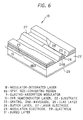
- FIG.6 shows the other modulator-integrated laser 1B used in the second preferred embodiment of the invention.
- the horizontal width of the spot size-reducing region 8 is slowly reduced from the incided end of the waveguide to the light-emitting end thereof in the first preferred embodiment shown FIGs.3 to 5
- the vertical width of the spot size-reducing region 8B is slowly reduced to narrow the beam width of the emitted light in the second preferred embodiment of the invention shown in FIG.6.
- the aspect ratio of the light-emitting end of the waveguide 24B is optimized, so that the shape of the emitted beam is almost an ideal Gaussian distribution.
- the modulator-integrated laser 1B is directly connected with the single mode optical fiber 3, a coupling loss therebetween is sufficiently low.
- the electro-absorption modulator is integrated with the DFB semiconductor laser to form a modulator-integrated laser on the same substrate, and the moduleted laser light emitted from the modulator-integrated laser is supplied to the outside via the optical fiber.
- the electro-absorption modulator is provided with the spot size-converting region formed of a tapered waveguide, the width of which is slowly reduced in the horizontal or vertical direction from the incident end of the waveguide to the light emitting end thereof.
- the spot size of the modulated laser light at the light-emitting end of the modulator-integrated laser is almost the same as that of the single mode optical fiber, hence both can be directly connected with a low coupling loss. Accordingly, there is no necessity for using optical components such as a lens, the fabrication cost can be reduced, and the time necessary for alignments of optical axes can be cut down.
- An electro-absorption modulator is integrated with a DFB semiconductor laser to form a modulator-integrated laser, and a modulated laser light emitted from the modulator-integrated laser is transmitted via an optical fiber.
- the electro-absorption modulator is provided with a spot size-converting region formed of a tapered waveguide, a width of which is slowly reduced in the horizontal direction from an incident end of the waveguide to the light-emitting end thereof.
- a spot size of the modulated laser light at a light-emitting end of the modulator-integrated laser is almost the same as that of the single mode optical fibre, hence both can be directly connected with a low coupling loss.
Landscapes
- Physics & Mathematics (AREA)
- Condensed Matter Physics & Semiconductors (AREA)
- General Physics & Mathematics (AREA)
- Electromagnetism (AREA)
- Optics & Photonics (AREA)
- Semiconductor Lasers (AREA)
- Optical Couplings Of Light Guides (AREA)
- Optical Integrated Circuits (AREA)
- Optical Modulation, Optical Deflection, Nonlinear Optics, Optical Demodulation, Optical Logic Elements (AREA)
Applications Claiming Priority (2)
| Application Number | Priority Date | Filing Date | Title |
|---|---|---|---|
| JP37450098 | 1998-12-28 | ||
| JP10374500A JP2000193921A (ja) | 1998-12-28 | 1998-12-28 | 変調器集積化レ―ザモジュ―ル |
Publications (2)
| Publication Number | Publication Date |
|---|---|
| EP1017141A2 true EP1017141A2 (de) | 2000-07-05 |
| EP1017141A3 EP1017141A3 (de) | 2000-11-15 |
Family
ID=18503957
Family Applications (1)
| Application Number | Title | Priority Date | Filing Date |
|---|---|---|---|
| EP99310572A Withdrawn EP1017141A3 (de) | 1998-12-28 | 1999-12-24 | Laservorrichtung mit integriertem Modulator |
Country Status (2)
| Country | Link |
|---|---|
| EP (1) | EP1017141A3 (de) |
| JP (1) | JP2000193921A (de) |
Cited By (4)
| Publication number | Priority date | Publication date | Assignee | Title |
|---|---|---|---|---|
| EP1217701A1 (de) * | 2000-12-20 | 2002-06-26 | Agilent Technologies, Inc. (a Delaware corporation) | Lichtmodulation |
| EP1263099A3 (de) * | 2001-05-17 | 2003-01-15 | Matsushita Electric Industrial Co., Ltd. | Halbleiterlaser |
| US7972879B2 (en) * | 2004-04-15 | 2011-07-05 | Binoptics Corporation | Multi-level integrated photonic devices |
| US8526478B2 (en) | 2010-06-10 | 2013-09-03 | Mitsubishi Electric Corporation | Semiconductor optical integrated element |
Families Citing this family (3)
| Publication number | Priority date | Publication date | Assignee | Title |
|---|---|---|---|---|
| KR100754597B1 (ko) | 2006-01-03 | 2007-09-05 | 삼성전자주식회사 | 광모드 크기 변환기 집적 레이저장치 및 그 제조방법 |
| JP6256311B2 (ja) * | 2014-11-17 | 2018-01-10 | 三菱電機株式会社 | 半導体光素子およびその製造方法 |
| JP6146554B1 (ja) * | 2017-01-19 | 2017-06-14 | 三菱電機株式会社 | 光変調器集積半導体レーザ |
Family Cites Families (1)
| Publication number | Priority date | Publication date | Assignee | Title |
|---|---|---|---|---|
| JP3104789B2 (ja) * | 1997-05-02 | 2000-10-30 | 日本電気株式会社 | 半導体光素子およびその製造方法 |
-
1998
- 1998-12-28 JP JP10374500A patent/JP2000193921A/ja active Pending
-
1999
- 1999-12-24 EP EP99310572A patent/EP1017141A3/de not_active Withdrawn
Cited By (6)
| Publication number | Priority date | Publication date | Assignee | Title |
|---|---|---|---|---|
| EP1217701A1 (de) * | 2000-12-20 | 2002-06-26 | Agilent Technologies, Inc. (a Delaware corporation) | Lichtmodulation |
| US6590693B2 (en) | 2000-12-20 | 2003-07-08 | Agilent Technologies, Inc. | Light modulation |
| EP1263099A3 (de) * | 2001-05-17 | 2003-01-15 | Matsushita Electric Industrial Co., Ltd. | Halbleiterlaser |
| US6865205B2 (en) | 2001-05-17 | 2005-03-08 | Matsushita Electric Industrial Co., Ltd. | Semiconductor laser |
| US7972879B2 (en) * | 2004-04-15 | 2011-07-05 | Binoptics Corporation | Multi-level integrated photonic devices |
| US8526478B2 (en) | 2010-06-10 | 2013-09-03 | Mitsubishi Electric Corporation | Semiconductor optical integrated element |
Also Published As
| Publication number | Publication date |
|---|---|
| JP2000193921A (ja) | 2000-07-14 |
| EP1017141A3 (de) | 2000-11-15 |
Similar Documents
| Publication | Publication Date | Title |
|---|---|---|
| US9148226B2 (en) | Optical module and optical transceiver installing the same | |
| US20040101020A1 (en) | Packaging and passive alignment of light source to single mode fiber using microlens and precision ferrule | |
| JPH09211272A (ja) | 光モジュール | |
| EP3997494B1 (de) | Hybride multiwellenlängenquelle und zugehörige verfahren | |
| US10680404B2 (en) | Optical subassembly, optical module, and optical transmission equipment | |
| US11353667B2 (en) | Transmitter optical sub-assembly (TOSA) structure and an active alignment method thereof | |
| US6876682B2 (en) | Light generating module | |
| EP1017141A2 (de) | Laservorrichtung mit integriertem Modulator | |
| US7018110B2 (en) | Optical module | |
| US7372879B2 (en) | Wavelength locker using modulator current and photodetector | |
| US20060006403A1 (en) | Optical module | |
| GB2370373A (en) | Alignment of optical assemblies | |
| JP5483677B2 (ja) | 半導体光通信モジュール及び、その製造方法 | |
| US20250337216A1 (en) | Laser beam emitting device and optical module | |
| US6572279B2 (en) | Light-emitting module | |
| JP2000156510A (ja) | 光半導体素子および光半導体素子の製造方法ならびに光電子装置 | |
| CA2320727A1 (en) | Laser modulators | |
| US20070147747A1 (en) | Optical module and optical transmission system using the same | |
| JP2003229636A (ja) | 半導体レーザ素子及び半導体レーザ装置 | |
| JP2022037163A (ja) | 光サブアセンブリ、光モジュール、及び光伝送装置 | |
| JPH05333248A (ja) | 波長分割多重方式送受信モジュール及びそれを用いた光伝送装置 | |
| CA2324808C (en) | Semiconductor laser module | |
| JPH0682660A (ja) | 光半導体モジュール | |
| US11112571B2 (en) | Optical subassembly | |
| US20010033720A1 (en) | System and method for aligning optical components |
Legal Events
| Date | Code | Title | Description |
|---|---|---|---|
| PUAI | Public reference made under article 153(3) epc to a published international application that has entered the european phase |
Free format text: ORIGINAL CODE: 0009012 |
|
| AK | Designated contracting states |
Kind code of ref document: A2 Designated state(s): FR GB |
|
| AX | Request for extension of the european patent |
Free format text: AL;LT;LV;MK;RO;SI |
|
| PUAL | Search report despatched |
Free format text: ORIGINAL CODE: 0009013 |
|
| AK | Designated contracting states |
Kind code of ref document: A3 Designated state(s): AT BE CH CY DE DK ES FI FR GB GR IE IT LI LU MC NL PT SE |
|
| AX | Request for extension of the european patent |
Free format text: AL;LT;LV;MK;RO;SI |
|
| RIC1 | Information provided on ipc code assigned before grant |
Free format text: 7H 01S 5/026 A, 7G 02B 6/12 B |
|
| 17P | Request for examination filed |
Effective date: 20001010 |
|
| 17Q | First examination report despatched |
Effective date: 20010613 |
|
| AKX | Designation fees paid |
Free format text: FR GB |
|
| REG | Reference to a national code |
Ref country code: DE Ref legal event code: 8566 |
|
| STAA | Information on the status of an ep patent application or granted ep patent |
Free format text: STATUS: THE APPLICATION IS DEEMED TO BE WITHDRAWN |
|
| 18D | Application deemed to be withdrawn |
Effective date: 20011228 |