EP1017146B1 - Protection contre les surcharges, chargeur, dispositif electronique et dispositif d'horloge - Google Patents
Protection contre les surcharges, chargeur, dispositif electronique et dispositif d'horloge Download PDFInfo
- Publication number
- EP1017146B1 EP1017146B1 EP99919643A EP99919643A EP1017146B1 EP 1017146 B1 EP1017146 B1 EP 1017146B1 EP 99919643 A EP99919643 A EP 99919643A EP 99919643 A EP99919643 A EP 99919643A EP 1017146 B1 EP1017146 B1 EP 1017146B1
- Authority
- EP
- European Patent Office
- Prior art keywords
- voltage
- turning
- switching
- circuit
- switching means
- Prior art date
- Legal status (The legal status is an assumption and is not a legal conclusion. Google has not performed a legal analysis and makes no representation as to the accuracy of the status listed.)
- Expired - Lifetime
Links
Images








Classifications
-
- H—ELECTRICITY
- H02—GENERATION; CONVERSION OR DISTRIBUTION OF ELECTRIC POWER
- H02M—APPARATUS FOR CONVERSION BETWEEN AC AND AC, BETWEEN AC AND DC, OR BETWEEN DC AND DC, AND FOR USE WITH MAINS OR SIMILAR POWER SUPPLY SYSTEMS; CONVERSION OF DC OR AC INPUT POWER INTO SURGE OUTPUT POWER; CONTROL OR REGULATION THEREOF
- H02M7/00—Conversion of AC power input into DC power output; Conversion of DC power input into AC power output
- H02M7/02—Conversion of AC power input into DC power output without possibility of reversal
- H02M7/04—Conversion of AC power input into DC power output without possibility of reversal by static converters
- H02M7/12—Conversion of AC power input into DC power output without possibility of reversal by static converters using discharge tubes with control electrode or semiconductor devices with control electrode
- H02M7/21—Conversion of AC power input into DC power output without possibility of reversal by static converters using discharge tubes with control electrode or semiconductor devices with control electrode using devices of a triode or transistor type requiring continuous application of a control signal
- H02M7/217—Conversion of AC power input into DC power output without possibility of reversal by static converters using discharge tubes with control electrode or semiconductor devices with control electrode using devices of a triode or transistor type requiring continuous application of a control signal using semiconductor devices only
- H02M7/219—Conversion of AC power input into DC power output without possibility of reversal by static converters using discharge tubes with control electrode or semiconductor devices with control electrode using devices of a triode or transistor type requiring continuous application of a control signal using semiconductor devices only in a bridge configuration
-
- H—ELECTRICITY
- H02—GENERATION; CONVERSION OR DISTRIBUTION OF ELECTRIC POWER
- H02J—ELECTRIC POWER NETWORKS; CIRCUIT ARRANGEMENTS OR SYSTEMS FOR SUPPLYING OR DISTRIBUTING ELECTRIC POWER; SYSTEMS FOR STORING ELECTRIC ENERGY
- H02J7/00—Circuit arrangements for charging or discharging batteries or for supplying loads from batteries
- H02J7/02—Circuit arrangements for charging or discharging batteries or for supplying loads from batteries for charging batteries from AC mains by converters
-
- H—ELECTRICITY
- H02—GENERATION; CONVERSION OR DISTRIBUTION OF ELECTRIC POWER
- H02J—ELECTRIC POWER NETWORKS; CIRCUIT ARRANGEMENTS OR SYSTEMS FOR SUPPLYING OR DISTRIBUTING ELECTRIC POWER; SYSTEMS FOR STORING ELECTRIC ENERGY
- H02J7/00—Circuit arrangements for charging or discharging batteries or for supplying loads from batteries
- H02J7/60—Circuit arrangements for charging or discharging batteries or for supplying loads from batteries including safety or protection arrangements
- H02J7/61—Circuit arrangements for charging or discharging batteries or for supplying loads from batteries including safety or protection arrangements against overcharge
-
- H—ELECTRICITY
- H02—GENERATION; CONVERSION OR DISTRIBUTION OF ELECTRIC POWER
- H02J—ELECTRIC POWER NETWORKS; CIRCUIT ARRANGEMENTS OR SYSTEMS FOR SUPPLYING OR DISTRIBUTING ELECTRIC POWER; SYSTEMS FOR STORING ELECTRIC ENERGY
- H02J7/00—Circuit arrangements for charging or discharging batteries or for supplying loads from batteries
- H02J7/80—Circuit arrangements for charging or discharging batteries or for supplying loads from batteries including monitoring or indicating arrangements
- H02J7/82—Control of state of charge [SOC]
Definitions
- the present invention relates to an overcharge prevention method and a charging circuit, suitable for preventing overcharge, and an electronic device and a timepiece, employing the overcharge prevention method and the charging circuit.
- a diode-bridge circuit In a charging circuit for charging a voltage storage device, such as a high-capacitance capacitor or a secondary battery, with an AC voltage generated by a generator, a diode-bridge circuit is typically employed as a rectifier circuit for full-wave rectifying the AC voltage.
- the diode-bridge circuit suffers from a loss due to a voltage drop through two diodes.
- a compact and portable electronic device such as a wristwatch, which employs a generator generating a small-amplitude AC voltage, is affected much by the loss through the diode-bridge circuit, and using the diode-bridge circuit as a rectifier circuit is not appropriate.
- FIG. 23 is a circuit diagram showing one example of a charging circuit employing a conventional synchronous rectifier circuit.
- the charging circuit includes comparators CMP1A and CMP1B, comparators CMP2A and CMP2B, P-channel FETs MP1 and MP2, N-channel FETs MN1 and MN2, and a high-capacitance capacitor C (charged device) for storing a charging current.
- the comparator CMP1A compares an output voltage V1 at an input terminal AG1 connected to a generator AG with a source voltage Vdd.
- the comparator CMP1B compares an output voltage V2 at an input terminal AG2 connected to the generator AG with the source voltage Vdd.
- the comparator CMP2A compares the output voltage V1 at the input terminal AG1 with a source voltage Vss.
- the comparator CMP2B compares the output voltage V2 at the input terminal AG2 with the source voltage Vss.
- the P-channel FET MP1 is turned on and off under the control of the comparator CMP1A, and the P-channel FET MP2 is turned on and off under the control of the comparator CMP1B,
- the N-channel FET MN1 is turned on and off under the control of the comparator CMP2A, and the N-channel FET MN2 is turned on and off under the control of the comparator CMP2B.
- D1-D4 are MOSFET parasitic diodes.
- FIG. 24 is a timing diagram illustrating the operation of the above-referenced charging circuit.
- the generator AG respectively outputs, at the input terminals AG1 and AG2, the output voltages V1 and V2 between which a phase difference of 180° occurs.
- the P-channel FET MP1 is turned on by the comparator CMP1A when the output voltage V1 of the generator AG becomes equal to or higher than the source voltage Vdd.
- the N-channel FET MN2 is turned on by the comparator CMP2B when the output voltage V2 of the generator AG becomes equal to or lower than the source voltage Vss.
- the P-channel FET MP2 is turned on by the comparator CM1B when the output voltage V2 of the generator AG becomes equal to or higher than the source voltage Vdd
- the N-channel FET MN1 is turned on by the comparator CMP2A when the output voltage V1 of the generator AG becomes equal to or lower than the source voltage Vss.
- a charging current i flows from the generator AG through arrow-headed paths into the high-capacitance capacitor C, charging the high-capacitance capacitor C, when both the P-channel FET MP1 and the N-channel FET MN2 are on, and when both the P-channel FET MP2 and the N-channel FET MN1 are on.
- the synchronous rectifier circuit employing the transistors performs full-wave rectification.
- the present invention has been developed in view of the above problem, and it is an object of the present invention to provide an overcharge prevention method, a charging circuit, an electronic device and a timepiece, for preventing overcharge and for preventing a shortcircuit of a voltage storage element associated with an overcharge prevention step.
- Japanese patent application no. JP-A-2-7834 discloses a charging apparatus for a battery located in a car.
- the charging apparatus comprises a bridge rectifier circuit having four diodes.
- a thyristor is turned on accordingly.
- the generated current is shorted at both terminals of the generator.
- Current flow is then through the thyristor and a diode on one half-cycle and through a different thyristor and a different diode on the other half-cycle.
- the document also describes a three-phase version, in which plural diodes and FETs constitute a full-wave rectifying circuit and the FETs are used to provide a short-circuiting path to prevent overcharge of the battery.
- JP 09131064 published on 16th May 1997, discloses a rectifying circuit including four comparators, which drive the gates of respective transistors.
- the transistors are configured in a bridge configuration, in which the commoned main electrodes of each pair of transistors are connected to respective input terminals, which are fed by an AC voltage source, while the non-commoned main electrodes of each pair of transistors are connected to ground and an output voltage rail, respectively.
- the comparator-FET configurations the peak AC voltage levels on the input terminals can be made to be equal to the ground and output voltage rail, respectively, thereby providing a full-wave bridge rectifier of high efficiency.
- an overcharge prevention method for preventing the overcharging of a voltage storage element connected to a bridge rectifier circuit, the method being as defined in claim 1.
- a charging circuit for charging a voltage storage element comprises the features set forth in claim 8, while an electronic device, as set out in claim 19, represents a third aspect of the invention.
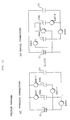
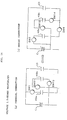
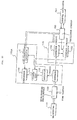
- FIG. 1 is a circuit diagram of the construction of a charging circuit illustrating an overcharge prevention method of the present invention.
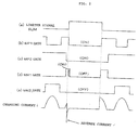
- FIG. 2 is a timing diagram illustrating the basic operation of the overcharge prevention method of the present invention.
- the charging circuit has a construction similar to that shown in FIG. 23, and like components are designated with like reference numerals.
- a charging circuit 100 includes a limiter circuit that blocks a charging current i to a high-capacitance capacitor C using a predetermined method to prevent overcharge to the high-capacitance capacitor C.
- the limiter circuit forms a closed loop path (see FIG. 1), different from a standard charging path, by turning on P-channel FETs MP1 and MP2, and prevents the high-capacitance capacitor C from being overcharged, by allowing an AC current from a generator AG to flow through the closed loop path.
- the limiter circuit turns on P-channel FETs MP1 and MP2 with N-channel FET MN1 or MN2 in an on state (hatched portion) in the construction shown in FIG. 1, as shown in FIG. 2, the high-capacitance capacitor C is short-circuited, causing a reverse current (short-circuit current) from the high-capacitance capacitor C, and power stored in the high-capacitance capacitor C is consumed in vain and furthermore, the high-capacitance capacitor C itself and a circuit section 7 are damaged.
- the overcharging of the high-capacitance capacitor C is prevented by on/off controlling P-channel FET MP1 or MP2, and furthermore, the generation of the short-circuit current by the high-capacitance capacitor C is prevented by on/off controlling the N-channel FETs MN1 and MN2, as well.
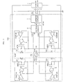
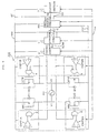
- FIG. 3 is a circuit diagram showing the construction of the charging circuit 100 of the first embodiment. Components identical to those described with reference to FIG. 23 are designated with the same reference numerals and the discussion about them is omitted here.
- a detector circuit 1 detects a charge voltage Va in the high-capacitance capacitor C and compares the charge voltage Va with an unshown predetermined reference voltage.
- the detector circuit 1 feeds a limiter signal SLIM to a control circuit 2 to prevent overcharge.
- control circuit 2 In response to the limiter signal SLIM, the control circuit 2 outputs a control signal CS1 having a rising edge delayed from the rising edge of the limiter signal SLIM and a control signal CS2 having a falling edge delayed from the falling edge of the limiter signal SLIM.
- An AND gate 3 is connected between a comparator CMP1A and P-channel FET MP1, and the control signal CS1 applied to an inverting input terminal of the AND gate 3 invalidates the output of the comparator CMP1A applied to the other input terminal of the AND gate 3.
- the AND gate 3 feeds an "L" level signal to the gate of the P-channel FET MP1, for the duration throughout which the control signal CS1 remains at an "H" level.
- An AND gate 4 is connected between a comparator and P-channel FET MP2, and the control signal CS1 applied to an inverting input terminal of the AND gate 4 invalidates the output of the comparator CMP1B applied to the other input terminal of the AND gate 4.
- the AND gate 4 feeds an "L" level signal to the gate of the P-channel FET MP2, for the duration throughout which the control signal CS1 remains at an "H" level.
- An AND gate 5 is connected between a comparator CMP2A and N-channel FET MN1, and the control signal CS2 applied to an inverting input terminal of the AND gate 5 invalidates the output of the comparator CMP2A applied to the other input terminal of the AND gate 5.
- the AND gate 5 feeds an "L" level signal to the gate of the N-channel FET MN1, at least for the duration throughout which the control signal CS2 remains at an "H" level.
- An AND gate 6 is connected between a comparator CMP2B and N-channel FET MN2, and the control signal CS2 applied to an inverting input terminal of the AND gate 6 invalidates the output of the comparator CMP2B applied to the other input terminal of the AND gate 6.
- the AND gate 6 feeds an "L" level signal to the gate of the N-channel FET MN2, at least for the duration throughout which the control signal CS2 remains at an "H" level.
- the control signal CS1 having a rising edge delayed from that of the limiter signal SLIM is fed to the inverting input terminals of the AND gate 3 and the AND gate 4, while the control signal CS2 having a falling edge delayed from that of the limiter signal SLIM is fed to the inverting input terminals of the AND gate 5 and the AND gate 6, and thus off time of the N-channel FETs MN1 and MN2 is set to be longer than on time of the P-channel FETs MP1 and MP2.
- the high-capacitance capacitor C is charged with power generated by the generator AG and full-wave rectified through a synchronous rectifier circuit, and feeds drive power to the circuit section 7.
- the high-capacitance capacitor C has a withstand voltage and has the characteristic that a charging in excess of the withstand voltage puts the capacitor C into an overcharged state, degrading the capacitor C and lowering its charging efficiency.
- the high-capacitance capacitor C is employed.
- the present invention is not limited to this, and alternatively, a secondary battery may be employed.
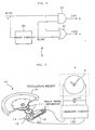
- FIG. 4 is a circuit block diagram showing one example of the above-described control circuit 2.
- a delay circuit 2a employing a capacitor or the like, delays the limiter signal SLIM, namely, the output of the detector circuit 1, by a predetermined time, and supplies one input terminal of an AND gate 2b and one input terminal of an OR gate 2c with the delayed limiter signal SLIM, referred to as a limiter signal SLIM'.
- the AND gate 2b ANDs the limiter signal SLIM and the delayed limiter signal SLIM', and outputs the resulting signal as the control signal CS1.
- the AND gate 2b outputs a signal having a rising edge which is delayed by a predetermined time from the rising edge of the limiter signal SLIM.
- the falling edge of the control signal CS1 coincides with the falling edge of the limiter signal SLIM.
- the OR gate 2c receives, at the other input terminal, the limiter signal SLIM, and ORs the limiter signal SLIM and the delayed limiter signal SLIM', and outputs the resulting signal as the control signal CS2.
- the OR gate 2c outputs a signal having a falling edge delayed by a predetermined time from the limiter SLIM.
- the rising edge of the control signal CS2 coincides with the rising edge of the limiter signal SLIM.
- FIG. 5 is a conceptual view roughly showing a (wrist watch) timepiece in which the charging circuit is incorporated.
- the generator AG includes a rotor 14 and a stator 15, and when the disklike rotor 14 having two magnetized poles rotates, an electromotive force occurs in an output coil 16 of the stator 15, and an AC current is thus picked up.
- an oscillating weight 13 turns in a wristwatch case, and a train wheel mechanism 11 transfers a turn motion of the oscillating weight 13 to the generator AG.
- the oscillating weight 13 turns as a person wearing the wristwatch swings his or her arm, and the generator AG provides power in response to the motion of the wristwatch.
- the AC power provided by the generator AG is full-wave rectified by the charging circuit 100 and charges the high-capacitance capacitor C.
- a processing section 9 drives a clocking unit 8 with power supplied from the high-capacitance capacitor C.
- the clocking unit 8 composed of a crystal oscillator, counter circuits, etc., frequency-divides a master clock signal, generated by the crystal oscillator, through the counter circuit, performs time measurement based on the frequency division result, and drives a stepping motor to turn hands.
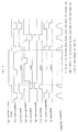
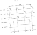
- FIG. 6 is a timing diagram illustrating the operation of the charging circuit 100 of the first embodiment. The ordinary charging operation remains unchanged from the one discussed referring to the timing diagram shown in FIG. 23, and the discussion about it is omitted here.
- the limiter signal SLIM is fed to the control circuit 2 to prevent overcharge when the detector circuit 1 detects that a charge voltage Va at the high-capacitance capacitor C becomes equal to or higher than a reference voltage (FIG. 6(a)).
- the control circuit 2 feeds the limiter signal SLIM to the delay circuit 2a while also feeding the limiter signal SLIM to the other input terminal of the AND gate 2b and the other input terminal of the OR gate 2c.
- the delay circuit 2a delays the limiter signal SLIM by a predetermined time, and feeds it as the limiter signal SLIM' to the one input terminal of the AND gate 2b and the one input terminal of the OR gate 2c.
- the control circuit 2 outputs the control signal CS1 that is transitioned to an "H” level with a delay time subsequent to the limiter signal SLIM, while outputting the control signal CS2 that is transitioned to an "H” level concurrently with the limiter signal SLIM (see FIGS. 6(a), 6(b) and 6(c)).
- the P-channel FETs MP1 and MP2 remain on, at least for a duration throughout which the control signal CS1 is at an "H" level (see FIGS. 6(e) and 6(g)). As a result, a closed loop path, different from the standard charging path, is formed as shown in FIG. 3.
- the N-channel FETs MN1 and MN2 remains off, at least for the duration throughout which the control signal CS2 is at an "H" level (see FIGS. 6(i) and 6(k)).
- the AC current from the generator AG flows through the arrow-headed closed loop path, the charging current i to the high-capacitance capacitor C is cut off, and overcharging of the high-capacitance capacitor C is thus prevented (see FIG. 6).
- the period T1 throughout which the control signal CS1 remains at an "H” level is compared with the period T2 throughout which the control signal CS2 remains at an "H” level, the period T2 throughout which the control signal CS2 remains at an "H” level is longer by the delay caused by the control circuit 2.
- the P-channel FETs MP1 and MP2 are turned on after the N-channel FETs MN1 and MN2 are turned off.
- the N-channel FETs MN1 and MN2 are restored to their normal operational state after the P-channel FETs MP1 and MP2 are restored to their normal operational state.
- the high-capacitance capacitor C is not shorted, no short-circuit current is caused, the power stored in the high-capacitance capacitor C is not consumed in vain, and the high-capacitance capacitor C and the circuit section 7 remain free from damage.
- the charging circuit performs automatic control in which the short-circuit current (limiter current ILIM) applies electromagnetic braking to the rotation of the rotor 14, causing terminal voltages V1 and V2 to drop, and reducing the short-circuit current (limiter current ILIM). As a result, the generation of electromagnetic noise in the rotor 14 is controlled.
- opening the charging path to the high-capacitance capacitor C is also contemplated.
- circuit elements P-channel FETs MP1 and MP2, N-channel FETs MN1 and MN2, comparators CMP1A, CMP1B, CMP2A, and CMP2B), and withstand voltages of these circuit elements must be increased.
- a charging circuit in a compact portable device such as a wristwatch
- a charging circuit in a compact portable device is constructed of integrated circuits using miniature circuit elements to promote miniaturization, increasing the withstand voltages is difficult.
- this embodiment forms the closed loop path through the input terminals AG1 and AG2 at the moment the charge voltage Va exceeds the predetermined voltage, and hence circuit elements with low withstand voltages work.
- the use of integrated circuits is facilitated, promoting miniaturization of the charging circuit.
- the closed loop path is formed by turning off the N-channel FETs MN1 and MN2 and then by turning on the P-channel FETs MP1 and MP2, when the charge voltage Va at the high-capacitance capacitor C exceeds the reference voltage.
- the charge voltage Va does not exceeds the withstand voltage of the high-capacitance capacitor C, and thereby the high-capacitance capacitor C is protected against overcharging.
- the high-capacitance capacitor C is not shorted, the power stored in the high-capacitance capacitor C is not consumed in vain, and the high-capacitance capacitor C and the circuit section 5 are protected against damage.
- the closed loop path different from the charging path, is formed, permitting the generated current to flow therethrough.
- the N-channel FETs MN1 and MN2 are forced to be off before the P-channel MP1 and MP2 are turned on.
- a closed loop path is formed by turning on the P-channel FETs MP1 and MP2 with the N-channel FETs MN1 and MN2 remaining off.
- FIG. 7 is a circuit diagram showing the construction of a charging circuit 101 of the second embodiment. Components identical to those described with reference to FIG. 3 are designated with the same reference numerals, and the discussion about them is omitted here.
- the charging circuit 101 is identical to the charging circuit 100 of the first embodiment but with the control circuit 2 removed therefrom and AND gates 20 and 21 newly added thereto.
- the limiter signal SLIM output by the detector circuit 1 is input to one input terminal of the AND gate 20, inverting input terminals of AND gates 5 and 6 and one input terminal of the AND gate 21.
- the output signal of the AND gate 5 namely, a signal applied to the gate of N-channel FET MN1, is fed to an inverting input terminal of the AND gate 20.
- the AND gate 20 feeds the limiter signal SLIM (at an "H” level) from the detector circuit 1 to an inverting input terminal of an AND gate 3 when the signal fed to the gate of the N-channel FET MN1 is at an "L” level, in other words, the N-channel FET MN1 is turned off.
- the P-channel FET MP1 is turned on in response to the limiter signal SLIM, only when the N-channel FET MN1 is turned off.
- the AND gate 21 feeds the limiter signal (at an "H” level) from the detector circuit 1 to the inverting input terminal of the AND gate 4 when the signal applied to the gate of the N-channel FET MN2 is at an "L” level, in other words, when the N-channel FET MN2 is off.
- the P-channel FET MP2 is turned on in response to the limiter signal SLIM, only when the N-channel FET MN2 is turned off.
- FIG. 8 is a timing diagram showing the operation of the charging circuit 101 of the second embodiment.
- the ordinary charging operation remains unchanged from the one discussed referring to the timing diagram shown in FIG. 23, and the discussion about it is omitted here.
- the detector circuit 1 supplies the limiter signal SLIM for preventing overcharge to the one input terminal of the AND gate 20, the inverting input terminals of the AND gates 5 and 6, and the one input terminal of the AND gate 21 (see FIG. 8(a)), when the detector circuit 1 detects that the charge voltage Va of the high-capacitance capacitor becomes equal to or higher than the reference voltage.
- the limiter signal SLIM (at an "H” level), applied to the AND gate 20, is fed to the inverting input terminal of the AND gate 3, turning on the gate of the P-channel FET MP1 (to an "L” level) (see FIG. 8(c)) and putting the P-channel FET MP1 into an on state.
- the limiter signal SLIM (at an "H” level), fed to the AND gate 21, is fed to the inverting input terminal of the AND gate 4.
- the gate of the P-channel FET MN2 is turned on (to an "L" level) (see FIG. 8(e)), and the P-channel FET MN2 is turned on. In this way, the P-channel FETs MP1 and MP2 are put into the on state, at least for the duration throughout which the N-channel FETs MN1 and MN2 are turned off.
- the closed loop path different from the normal charging path, is formed, the AC current (limiter current ILIM) of the generator AG flows as represented by the arrow-headed closed loop paths, the charging current to the high-capacitance capacitor C is cut off, and the high-capacitance capacitor C is protected against overcharging. Throughout this period, the N-channel FETs MN1 and MN2 are necessarily off, no short-circuit current by the high-capacitance capacitor C is caused, and the high-capacitance capacitor C and the circuit section 7 remain free from damage.
- FIG. 9 is a circuit diagram showing the construction of a charging circuit 102 of a third embodiment. As shown in FIG. 9, components identical to those described with reference to FIG. 3 are designated with the same reference numerals, and the discussion about them is omitted here.
- the difference between the charging circuit 102 of the third embodiment and the charging circuit 100 of the first embodiment shown in FIG. 3 lies in that the charging circuit 102 includes a voltage multiplier circuit 49 for producing increased drive voltage VSS by multiplying an output voltage VSS' of the high-capacitance capacitor C and auxiliary capacitor CS charged with the increased voltage VSS so that the increased drive voltage VSS is fed to a rectification control circuit composed of the circuit section 7, detector circuit 1, control circuit 2, comparators CMP1A, CMP1B, CMP2A, and CMP2B, and AND gates 3, 4, 5, and 6.
- the voltage multiplier circuit 49 includes a switch SW1, one terminal of which is connected to a high-voltage terminal of the high-capacitance capacitor C, a switch SW2, one terminal of which is connected to the other terminal of the switch SW1, and the other terminal of which is connected to a low-voltage terminal of the high-capacitance, secondary power source 48, a capacitor 49a, one terminal of which is connected to the junction of the switch SW1 and switch SW2, a switch SW3, one terminal of which is connected to the other terminal of the capacitor 49a, and the other terminal of which is connected to the low-voltage terminal of the high-capacitance, secondary power source 48, a switch SW4, one terminal of which is connected to a low-voltage terminal of an auxiliary capacitor CS, and the other terminal of which is connected to the junction of the capacitor 49a and the switch SW3, a switch SW11, one terminal of which is connected to the junction of the high-voltage terminal of the high-capacitance, secondary power source 48 and a high-
- the operation of the third embodiment remains unchanged from that of the first embodiment, except for the operational voltages (VSS' and VSS), and the following discussion focuses on the operation of the voltage multiplier circuit and its associated circuits.
- the operation of the voltage multiplier circuit 49 is discussed in connection with a voltage tripler mode, a voltage doubler mode, a one-and-half-time voltage multiplier mode, an original voltage mode (short mode) and an original voltage mode (charge transfer mode).
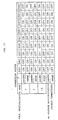
- the voltage multiplier circuit 49 operates in response to a voltage multiplication clock CKUD input from outside, and, at a first voltage multiplication timing (parallel connection timing), turns switch SW1 on, switch SW2 off, switch SW3 on, switch SW4 off, switch SW11 on, switch SW12 off, switch SW13 on, switch SW14 off, and switch SW21 off as shown in FIG. 11 during a voltage tripler mode.
- the equivalent circuit of the voltage multiplier circuit 49 in this case is shown in FIG. 12(a), and the capacitor 49a and the capacitor 49b are supplied with power from the high-capacitance capacitor C and are continuously charged until the voltage of each of the capacitor 49a and the capacitor 49b becomes substantially equal to that of the high-capacitance capacitor C.
- the voltage multiplier circuit 49 turns switch SW1 off, switch SW2 on, switch SW3 off, switch SW4 off, switch SW11 off, switch SW12 off, switch SW13 off, switch SW14 on, and switch SW21 on.
- the voltage multiplier circuit 49 operates in response to a voltage multiplication clock CKUD input from outside, and, at a first voltage multiplication timing (parallel connection timing), turns switch SW1 on, switch SW2 off, switch SW3 on, switch SW4 off, switch SW11 on, switch SW12 off, switch SW13 on, switch SW14 off, and switch SW21 off as shown in FIG. 11 during a voltage doubler mode.
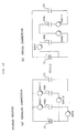
- the equivalent circuit of the voltage multiplier circuit 49 in this case is shown in FIG. 13(a), and the capacitor 49a and the capacitor 49b are supplied with power from the high-capacitance capacitor C and are continuously charged until the voltage of each of the capacitor 49a and the capacitor 49b becomes substantially equal to that of the high-capacitance capacitor C.
- the voltage multiplier circuit 49 turns switch SW1 off, switch SW2 on, switch SW3 off, switch SW4 on, switch SW11 off, switch SW12 on, switch SW13 off, switch SW14 on, and switch SW21 off.
- the equivalent circuit of the voltage multiplier circuit 49 in this case is shown in FIG. 13(b), the high-capacitance capacitor C is connected in series with each of the capacitor 49a and capacitor 49b, the auxiliary capacitor CS is charged with the voltage twice as large as the voltage of the high-capacitance capacitor C, and hence the double voltage is thus obtained.
- the voltage multiplier circuit 49 operates in response to a voltage multiplication clock CKUD input from outside, and, at a first voltage multiplication timing (parallel connection timing), turns switch SW1 on, switch SW2 off, switch SW3 off, switch SW4 off, switch SW11 off, switch SW 12 off, switch SW13 on, switch SW14 off, and switch SW21 on as shown in FIG. 11 during a one-and-half-time voltage multiplier mode.
- the equivalent circuit of the voltage multiplier circuit 49 in this case is shown in FIG. 14(a), and the capacitor 49a and the capacitor 49b are supplied with power from the high-capacitance capacitor C and are continuously charged until the voltage of each of the capacitor 49a and the capacitor 49b becomes substantially equal to half the voltage of the high-capacitance capacitor C.
- the voltage multiplier circuit 49 turns switch SW1 off, switch SW2 on, switch SW3 off, switch SW4 on, switch SW11 off, switch SW12 on, switch SW 13 off, switch SW14 on, and switch SW21 off.
- the equivalent circuit of the voltage multiplier circuit 49 in this case is shown in FIG. 14(b), the high-capacitance capacitor C is connected in series with both the capacitor 49a and capacitor 49b connected in parallel, the auxiliary capacitor CS is charged with the voltage one and half times as large as the voltage of the high-capacitance capacitor C, and hence the one-and-half-time voltage is thus obtained.
- the voltage multiplier circuit 49 turns switch SW1 off, switch SW2 on, switch SW3 on, switch SW4 on, switch SW11 off, switch SW12 on, switch SW13 on, switch SW14 on, and switch SW21 off as shown in FIG. 11 during an original voltage mode.
- FIG. 15(a) The connection of the voltage multiplier circuit 49 is shown in FIG. 15(a), and its equivalent circuit is shown in FIG. 15(b), wherein the high-capacitance capacitor C is directly connected with the auxiliary capacitor CS.
- the increased drive voltage VSS is supplied to the rectification control circuit composed of the circuit section 7, detector circuit 1, control circuit 2, comparators CMP1A, CMP1B, CMP2A, and CMP2B, and AND gates 3, 4, 5, and 6, and even if the voltage VSS' of the high-capacitance capacitor C (corresponding the voltage at the high-voltage terminal in this embodiment) is low, the increased voltage VSS is reliably supplied, and the circuit section 7 is thus stably driven.
- control voltages supplied to rectifying transistors P-channel FETs MP1 and MP2 and N-channel FETs MN1 and MN2 become low when the voltage VSS' in the high-capacitance capacitor C becomes low, and the charging efficiency drops.
- the increased power source voltage VSS multiplied from the power source voltage VSS', drives the P-channel FETs MP1 and MP2 and N-channel FETs MN1 and MN2, and hence the on-state resistance of each transistor is decreased.
- drain current Ids is expressed in the following equation, and increases in proportion to the square of gate voltage Vgs.
- Vgs gate voltage
- FIG. 16 is a circuit diagram of a charging circuit 103 of a fourth embodiment.
- components identical to those described in connection with FIG. 3 for the first embodiment are designated with the same reference numerals, and the discussion about them is omitted here.
- the difference between the charging circuit 103 of the fourth embodiment and the charging circuit 100 of the first embodiment is that a voltage multiplier circuit 49A is inserted between an AND gate 3 and P-channel FET MP1, and that a voltage multiplier circuit 49A is inserted between an AND gate 4 and P-channel FET MP2.
- the voltage multiplier circuit 49A is different from the voltage multiplier circuit 49 in that the voltage multiplier circuit 49 has a variable voltage multiplication rate so that the increased power source voltage VSS falls within a predetermined voltage range while the fourth embodiment fixes the voltage multiplication rate (of 2, for example).
- the voltage multiplier circuit 49A takes the equivalent circuit having a voltage multiplication rate of 2 as shown in FIG. 13.
- the detector circuit 1 supplies the limiter signal SLIM for preventing overcharge to the control circuit 2, when the absolute value of charge voltage Va of the high-capacitance capacitor C becomes equal to or higher than the reference voltage.
- the control circuit 2 feeds the limiter signal SLIM to the delay circuit 2a (see FIG. 4), the other input terminal of the AND gate 2b and the other input terminal of the OR gate 2c.
- the delay circuit 2a delays the limiter signal by a predetermined time, and feeds the delayed signal, as a limiter signal SLIM', to one input terminal of the AND gate 2b and one input terminal of the OR gate 2c.
- the control circuit 2 outputs, to the voltage multiplier circuit 49, the control signal CS1 that is transitioned to an "H" level with a predetermined time delay from the limiter signal SLIM and outputs, to the N-channel FETs MN1 and MN2, the control signal CS2 which is transitioned to an "H” level at the same timing as the limiter signal SLIM.
- the voltage multiplier circuit 49A multiplies the control signal CS2 at a fixed voltage multiplication rate (of 2, for example), and feeds the voltage-multiplied signal CS2 to the P-channel FETs MP1 and MP2.
- the P-channel FETs MP1 and MP2 remain in an on state, at least for a duration throughout which the control signal CS1 is at an "H" level.
- the closed loop path, different from the ordinary charging path, is thus formed, as shown in FIG. 3.
- the N-channel FETs MN1 and MN2 remain in an off state, at least for a duration throughout which the control signal CS2 is at an "H" level.
- the AC current of the generator AG flows along the arrow-headed closed loop paths, the charging current i to the high-capacitance capacitor C is cut off, and the overcharging of the high-capacitance capacitor C is thus precluded.
- the voltage multiplier circuit 49A multiplies voltage at a fixed voltage multiplication rate to drive rectifying transistors, namely, P-channel FETs MP1 and MP2, regardless of the voltage supplied to the circuit section 7.
- the fourth embodiment thus provides a higher rectification efficiency than the third embodiment.
- the period T1 throughout which the control signal CS1 remains at an "H” level is compared with the period T2 throughout which the control signal CS2 remains at an "H” level, the period T2 throughout which the control signal CS2 remains at an "H” level is longer by the delay caused by the control circuit 2.
- the P-channel FETs MP1 and MP2 are turned on after the N-channel FETs MN1 and MN2 are turned off.
- the N-channel FETs MN1 and MN2 are restored to their normal operational state after the P-channel FETs MP1 and MP2 are restored to their normal operational state.
- the high-capacitance capacitor C is not shorted, no short-circuit current is caused, the power stored in the high-capacitance capacitor C is not consumed in vain, and the high-capacitance capacitor C and the circuit section 7 remain free from damage.
- the fourth embodiment further offers improved rectification efficiency, besides the advantages of the third embodiment.
- the detector circuit 1 in the first through fourth embodiments is replaced with a detector circuit 1A for performing sampling detection operation.
- FIG. 17 shows the construction of the detector circuit 1A of the fifth embodiment.
- the detector circuit 1A includes a voltage divider 50, which voltage divides the voltage Va of the high-capacitance capacitor C to obtain detected voltage Va' proportional to the voltage Va, a reference voltage generator circuit 51 for generating a reference voltage Vref, a comparator 52 for outputting an original limiter signal SLIM0 by comparing the detected voltage Va' with the reference voltage Vref, a latch circuit 53 for latching and holding the original limiter signal SLIM0 at a timing corresponding to a sampling signal SS3 to output a limiter signal SLIM1, a switch SW51 for feeding power to the reference voltage generator circuit 51 in accordance with a sampling signal SS1, a switch SW52 for feeding power to the comparator 52 in accordance with a sampling signal SS2, and a switch SW53 for connecting the voltage divider 50 to the high-capacitance capacitor C in accordance with the sampling signal SS3.
- a voltage divider 50 which voltage divides the voltage Va of the high-capacitance capacitor C to obtain detected voltage Va' proportional
- sampling signal SS1, sampling signal SS2, and sampling signal SS3 are as follows: sampling signal SS1 ⁇ sampling signal SS2 ⁇ sampling signal SS3.
- the reference voltage generator circuit 51 which takes time most before reaching its stable operation, is supplied with power, and the comparator 52 is then supplied with power.
- the voltage divider 50 is connected to the high-capacitance capacitor C, and the latch circuit 53 receives the original limiter signal SLIM0.
- transition timings are successively shifted in the order of sampling signal SS1 ⁇ sampling signal SS2 ⁇ sampling signal SS3, although the transition timings of the sampling signals SS1, SS2 and SS3 are shown as being at the same timing, for simplicity, as shown in FIG. 19.
- step S 1 When it is determined in step S 1 that the elapsed time T from the preceding sampling timing is shorter than the sampling period Tsp (No in step S1), the process goes to standby state, in which step S1 is repeated.
- step S1 When it is determined in step S1 that the elapsed time T from the preceding sampling timing is equal to or longer than the sampling period Tsp (Yes in step S1), the sampling signal SS1, sampling signal SS2 and sampling signal SS3 are successively transitioned from an "L" level to an "H” level at each of t1, t3 and t4 as shown in FIG. 19. Specifically, the switch SW51, switch SW52, and switch SW53 are successively turned on.
- the reference voltage generator circuit 51 is powered, the comparator 52 is then powered, and when the reference voltage Vref and the operation of the comparator 52 become stabilized, the voltage divider 50 is connected to the high-capacitance capacitor C, and the comparator 52 determines whether the detected voltage Va' exceeds the reference voltage Vref (step S2).
- step S2 When it is determined in step S2 that the detected voltage Va' is above the reference voltage Vref with the original limiter signal SLIM0 at an "H” level for a duration from t2 to t5 as shown in FIG. 19 (Yes in step S2), the latch circuit 53 picks up the original limiter signal SLIM0 at an "H” level at t3 and t4 in FIG. 19, and the limiter signal SLIM1 is transitioned to an "H” level (step S3).
- the control circuit 2 outputs the control signal CS2 to turn off the N-channel FETs MN1 and MN2 (step S4), and determines whether the N-channel FETs MN1 and MN2 have been turned off (step S5).
- step S5 When it is determined in step S5 that at least one of the N-channel FETs MN1 and MN2 is turned on (No in step S5), the process returns to step S4, where the control signal CS1 is output to turn off the N-channel FETs MN1 and MN2.
- step S5 When it is determined in step S5 that both FETs MN1 and MN2 are turned on (Yes in step S5), the P-channel FETs MP1 and MP2 are turned on (step S6), and the process returns to step S1 to repeat the above steps.
- step S2 When it is determined in step S2 that the detected voltage Va' is below the reference voltage Vref with the original limiter signal SLIM0 at an "L" level for a duration from t1 to t2 or from t5 thereafter as shown in FIG. 19 (No in step S2), the latch circuit 53 picks up the original limiter signal SLIM0 at an "L” level at t1 and t6 in FIG. 19, and the limiter signal SLIM1 is transitioned to an "L” level (step S7), and the process returns to step S1 to repeat the above steps.
- the operation of the detector circuit 1A is intermittently performed in accordance with the sampling signals, the power consumption involved in detection is reduced.
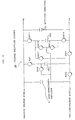
- FIG. 20 shows the construction of a detector circuit of a sixth embodiment of the present invention.
- the detector circuit 1B includes a constant current source CCNST, one end of which is connected to a power source VDD, a transistor Q1, the drain D and the gate G of which are connected together to the other end of the constant current source CCNST, a transistor Q2, the drain D and the gate G of which are connected together to the source S of the transistor Q1, a pull-up resistor RPU, one end of which is connected to the power source VDD, an inverter INV1, the input terminal of which is connected to the other end of the pull-up resistor RPU, for outputting a limiter signal SLIM, and a current mirror circuit CMC connected to the source S of the transistor Q2, the other end of the pull-up resistor RPU and a power source VSS.
- a constant current source CCNST one end of which is connected to a power source VDD
- a transistor Q1 the drain D and the gate G of which are connected together to the other end of the constant current source CCNST
- a transistor Q2 the drain D and the gate G
- the current mirror circuit CMC includes a transistor QD, the drain D and the gate G of which are connected together to the source S of the transistor Q2, and the source S of which is connected to the power source VSS, and a transistor QC, the drain D of which is connected to the other end of the pull-up resistor RPU, the gate G of which is connected to the gate G of the transistor QD, and the source S of which is connected to the power source VSS.
- a power source voltage (VSS'-VDD) is in a low range, in other words, lower than the sum of threshold voltages of the transistor Q1, transistor Q2, and transistor QD, no current flows from the constant current source CCNST, and the transistor QD and the transistor QC in the current mirror circuit CMC remain off.
- a voltage V1 (corresponds to an "H” level), pulled up to the power source VDD through the pull-up resistor RPU, is fed to the input terminal of the first inverter INV1, and the first inverter INV1 outputs the limiter signal SLIM at an "L" level, keeping a limiter transistor 40 in an off state.
- the current flowing through the transistor QC is set to be larger than the current flowing through the pull-up resistor RPU, and as a result, the voltage V1 corresponds to an "L" level.
- the first inverter INV1 outputs an "H" level signal, turning the limiter transistor 40 on and thereby permitting the limiter current to flow.
- the voltage detector circuit 1B in the sixth embodiment consumes almost no current when the power source voltage is low, and properly serves as a circuit for preventing excessive voltage in a portable electronic device operated from a battery.
- the electronic device employing charging circuit 100 or 101 is a wristwatch, but the present invention is not limited to this.
- the present invention may be implemented in a pocket timepiece, a table clock, a calculator, a portable personal computer, an electronic pocketbook, a portable radio, a portable tonometer, a portable telephone, a pager, a pedometer, etc.
- the present invention may be implemented in any electronic device that consumes power. In such an electronic device, internal electronic circuits and mechanisms are continuously used even with no battery employed.
- the electronic device may be used any time, and is free from the replacement of batteries and does not present problems arising from the disposal of batteries.
- a non-rechargeable battery may be used as the charging circuit 100, 101, 102 or 103, and when an electronic device is left unused, e.g. is not carried for a long period of time, the electronic device may be immediately operated from power from the battery, and as a user carries the electronic device, power is generated, allowing the electronic device to operate.
- the closed loop path is formed by turning on the P-channel FETs P1 and P2.
- a closed loop path may be formed by turning on the N-channel FETs N1 and N2.
- unipolar transistors such as P-channel FETs P1 and P2 and N-channel FETs N1 and N2 are employed as switching means.
- P-channel FETs P1 and P2 may be replaced with PNP transistors
- N-channel FETs N1 and N2 may be replaced with NPN bipolar transistors.
- the saturation voltage between emitter and collector is typically 0.3 V, and when the voltage generated by the generator AG is small, FETs are preferable as in the above embodiments.
- comparators CMP1A , CMP1B , CMP2A , and CMP2B may respectively be constructed of FETs, and each of the charging circuits 100, 101, 102, and 103 may be formed in an one chip integrated circuit.
- parasitic diodes D1-D4 of integrated P-channel FET P1, P-channel FET P2, N-channel FET N1 and N-channel FET N2 allows the rectification operation to continue even when the comparators fail to work with the power source voltage dropping.
- the generator AG is an electromagnetic generator in which the rotary motion of the oscillating weight 13 is transferred to the rotor 14 , and the electromotive force is generated in the output coil in response to the rotation of the rotor 14.
- the present invention is not limited this.
- acceptable as the generator AG may be the one in which a rotary motion, caused by a restoring force, generates an electromotive force, or the one in which external or self-oscillating, vibration or displacement, is applied to a piezo-electric body to generate power through the piezo-electric effect. In other words, any generator generating AC power works.
- a charging circuit may be arranged with the high-voltage side power line VDD and the low-voltage side power line VSS' reversed.
- the charging circuit in each of the above embodiments and the charging circuits in the above modifications may be incorporated in an electronically-controlled mechanical watch having a generator with a mainspring.
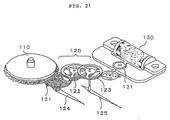
- FIG. 21 is a perspective view showing the mechanical structure of the electronically-controlled mechanical watch.
- a mainspring 110 is connected to a crown (not shown). By winding the crown, mechanical energy is stored in the mainspring 110.
- Accelerating train wheels 120 are arranged between the mainspring 110 and a rotor 131 of a generator 130.
- the accelerating train wheels 120 include center wheel and pinion 121, to which a minute hand 124 is connected, third wheel and pinion 122, and second wheel and pinion 123, to which a second hand 125 is connected.
- the accelerating train wheels 120 transfer the motion of the mainspring 110 to the rotor 131 of the generator 130 to cause the generator 130 to generate power.
- the generator 130 works as an electromagnetic brake to cause the hands connected to the accelerating train wheels 120 to rotate at a constant speed. In this sense, the generator 130 also works as a governor.
- FIG. 22 is an electrical block diagram showing the electronically-controlled mechanical watch, in which the charging circuit 100A, having a structure identical to that of the charging circuit 100 of the first embodiment, is incorporated.
- the charging circuit 100A includes the generator 130 and the rectifier 135.
- An oscillator circuit 160 generates a clock signal CLK using a crystal oscillator 161.
- a control circuit 103 controls a closed loop forming section 140, by adjusting the electromagnetic brake in accordance with the frequency detection result to make the rotational period of the rotor 131 coincide with the period of the clock signal CLK and to keep constant the rotational speed of the rotor 131.
- the closed loop forming section 140 switches on and off a closed loop path formed between both terminals of a coil of the AC generator AG.
- This switching function is performed by the P-channel transistors MP1 and MP2 in the above-referenced embodiments.
- a short-circuit braking is applied to the AC generator AG at a switch-on, and electric energy is stored in the coil of the AC generator AG.
- the AC generator AG operates, releasing the electric energy stored in the coil, and thereby generating an voltage. Since the electric energy at the switch-off is added to this voltage, its magnitude is increased.
- the closed loop path is formed by a short-circuit.
- a resistor may be added in series.
- a loop current flowing through the loop may be set to an optimum value.
- a predetermined pair of transistor pair out of the four rectifying transistors connected in a bridge, is turned on when a charge voltage exceeds a predetermined voltage so that the closed loop path is formed to allow the generated current to flow therethrough.
- the closed loop path is reliably formed, and the charged device is reliably prevented from being overcharged.
- the charged device Since the other transistor pair is turned on with the predetermined transistor pair off in the formation of the closed loop path, the charged device is reliably prevented from being overcharged.
- MOSFETs for the rectifying bridge circuit also serve as MOSTFETs for the overcharge prevention circuit, available space of the electronic device, such as a wristwatch, in which space saving requirement is rigorous, is fully exploited, and the manufacturing cost for the device is also reduced.
Landscapes
- Engineering & Computer Science (AREA)
- Power Engineering (AREA)
- Charge And Discharge Circuits For Batteries Or The Like (AREA)
- Electromechanical Clocks (AREA)
- Rectifiers (AREA)
- Electric Clocks (AREA)
- Control Of Charge By Means Of Generators (AREA)
- Direct Current Feeding And Distribution (AREA)
Claims (22)
- Procédé de prévention des surcharges pour prévenir la surcharge d'un élément d'accumulation de tension (C) raccordé à un circuit redresseur à pont comprenant une première section de commutation (MP) raccordée entre une première borne d'entrée (AG1) alimentée avec une tension alternative et une première ligne d'alimentation (Vdd), une deuxième section de commutation (MP2) raccordée entre une deuxième borne d'entrée (AG2) alimentée par la tension alternative et la première ligne d'alimentation (Vdd), une troisième section de commutation (MN1) raccordée entre la première borne d'entrée (AG1) et la deuxième ligne d'alimentation (Vss), et une quatrième section de commutation (MN2) raccordée entre la deuxième borne d'entrée (AG2) et la deuxième ligne d'alimentation (Vss),
le procédé comprenant les étapes suivantes :
au cours d'une phase de charge, établissement du contact pour la première et la quatrième section de commutation, et coupure du contact pour la deuxième et la troisième section de commutation, ou établissement du contact pour la deuxième et de la troisième section de commutation, et coupure du contact pour la première et la quatrième section de commutation, en chargeant de la sorte l'élément d'accumulation de tension, et au cours d'une phase de protection contre les surcharges, établissement du contact pour la première et la deuxième section de commutation après avoir coupé le contact de la troisième et de la quatrième section de commutation, ou bien établissement du contact pour la troisième et de la quatrième section de commutation après avoir coupé le contact de la première et de la deuxième section de commutation, en formant de la sorte un chemin en boucle fermée entre la première et la deuxième borne d'entrée sans occasionner en même temps une décharge de l'élément d'accumulation de tension. - Procédé de prévention des surcharges selon la revendication 1, comprenant l'étape de fourniture de la première et de la deuxième section de commutation en tant que transistors MOS à effet de champ à canal P, et la troisième et la quatrième section de commutation en tant que transistors MOS à effet de champ à canal N.
- Procédé de prévention des surcharges selon la revendication 1, comprenant les étapes suivantes :comparaison (CMP1A) d'une tension aux bornes au niveau de la première borne d'entrée avec une tension dé sortie au niveau de la première ligne d'alimentation, et établissement et coupure du contact en conséquence pour la première section de commutation ;comparaison (CMP1B) d'une tension aux bornes au niveau de la deuxième borne d'entrée avec une tension de sortie au niveau de la première ligne d'alimentation, et établissement et coupure du contact en conséquence pour la deuxième section de commutation ;comparaison (CMP2A) d'une tension aux bornes au niveau de la première borne d'entrée avec une tension de sortie au niveau de la deuxième ligne d'alimentation, et établissement et coupure du contact en conséquence pour la troisième section de commutation ;comparaison (CMP2B) d'une tension aux bornes au niveau de la deuxième borne d'entrée avec une tension de sortie au niveau de la deuxième ligne d'alimentation, et établissent et coupure du contact en conséquence pour la quatrième section de commutation ;détection (1) de la tension chargée au niveau de l'élément d'accumulation de tension,détermination du fait si la tension de charge détectée dépasse une tension prédéfinie,coupure du contact de la première et de la deuxième section de commutation, lorsque la tension de charge dépasse une tension prédéfinie, et formation subséquente du chemin en boucle fermée entre la première et la deuxième borne d'entrée en établissant le contact pour la troisième et la quatrième section de commutation, oucoupure du contact de la troisième et de la quatrième section de commutation, lorsque la tension de charge dépasse la tension prédéfinie, et formation subséquente du chemin en boucle fermée entre la première et la deuxième borne d'entrée en établissant le contact pour la première et la deuxième section de commutation.
- Procédé de prévention des surcharges selon la revendication 3, où l'étape de détermination pour déterminer si la tension de charge détectée dépasse la tension prédéfinie, comprend une étape de comparaison pour comparer la tension de charge avec une tension de référence, la tension prédéfinie étant la tension de référence.
- Procédé de prévention des surcharges selon la revendication 3, comprenant une étape consistant à faire revenir la troisième et la quatrième section de commutation à une opération de charge normale, après avoir fait revenir la première et la deuxième section de commutation, lorsque l'on a fait revenir la troisième à la quatrième section de commutation au fonctionnement de charge normal.
- Procédé de prévention des surcharges selon la revendication 3, comprenant une étape consistant à faire revenir la première et la deuxième section de commutation à un fonctionnement de charge normal, après avoir fait revenir la troisième et la quatrième section de commutation, lorsque l'on a fait revenir les première à quatrième sections de commutation au fonctionnement de charge normal.
- Procédé de prévention des surcharges selon la revendication 3, où, lors de l'étape de détection pour détecter la tension de charge au niveau de l'élément d'accumulation de tension, la détection de la tension de charge est réalisée de manière intermittente selon une période d'échantillonnage prédéfinie.
- Circuit de charge pour charger un élément d'accumulation de tension, comprenant :caractérisé par :un premier moyen de commutation (MP1) raccordé entre une première borne d'entrée (AG1) alimentée par une tension alternative et une première ligne d'alimentation (Vdd),un deuxième moyen de commutation (MP2) raccordé entre une deuxième borne d'entrée (AG2) alimentée par la tension alternative et la première ligne d'alimentation (Vdd),un troisième moyen de commutation (MN1) raccordé entre la première borne d'entrée (AG1) et la deuxième ligne d'alimentation (Vss),un quatrième moyen de commutation (MN2) raccordé entre la deuxième borne d'entrée (AG2) et la deuxième ligne d'alimentation (Vss),un élément d'accumulation de tension (C) raccordé à un circuit redresseur à pont comprenant le premier moyen de commutation (MP1), le deuxième moyen de commutation (MP2), le troisième moyen de commutation (MN1), et le quatrième moyen de commutation (MN2),un moyen de régulation de la charge (2) afin de, au cours d'une phase de charge, établir le contact pour la première et la quatrième section de commutation et couper le contact pour la deuxième et la troisième section de commutation, ou établir le contact pour la deuxième et la troisième section de commutation et couper le contact pour la première et la quatrième section de commutation, en chargeant de la sorte l'élément d'accumulation de tension,
un moyen de formation d'une boucle fermée (2-6, CMP1A/B) pour, lors d'une phase de protection contre les surcharges, établir le contact pour la première et la deuxième section de commutation après avoir coupé le contact pour la troisième et la quatrième section de commutation, ou établir le contact pour la troisième et la quatrième section de commutation après avoir coupé le contact pour la première et la deuxième section de commutation, en formant de la sorte un chemin en boucle fermée entre la première et la deuxième borne d'entrée sans occasionner simultanément une décharge de l'élément d'accumulation de tension. - Circuit de charge selon la revendication 8, comprenant :un premier moyen comparateur (CMP1A) pour comparer une tension aux bornes alimentant la première borne d'entrée, avec une tension de sortie au niveau de la première ligne d'alimentation, et pour établir et couper le contact en conséquence pour le premier moyen de commutation (MP1) ;un deuxième moyen comparateur (CMP1B) pour comparer une tension aux bornes alimentant la deuxième borne d'entrée, avec la tension de sortie au niveau de la première ligne d'alimentation, et pour établir et couper le contact en conséquence pour le deuxième moyen de commutation (MP2) ;un troisième moyen comparateur (CMP2A) pour comparer une tension aux bornes alimentant la première borne d'entrée, avec la tension de sortie au niveau de la deuxième ligne d'alimentation, et pour établir et couper le contact en conséquence pour le troisième moyen de commutation (MN1) ;un quatrième moyen comparateur (CMP2B) pour comparer une tension aux bornes alimentant la deuxième borne d'entrée, avec la tension de sortie au niveau de la deuxième ligne d'alimentation, et pour établir et couper le contact en conséquence pour le quatrième moyen de commutation (MN2) ; etun moyen comparateur de la tension prédéfinie (1), qui détecte une tension chargée au niveau de l'élément d'accumulation de tension, et qui détermine si la tension de charge détectée dépasse une tension prédéfinie, oùle moyen de formation de la boucle fermée est disposé de manière à former le chemin en boucle fermée entre la première borne d'entrée et la deuxième borne d'entrée en coupant le contact pour le troisième et le quatrième moyen de commutation et en établissant de manière subséquente le contact pour le premier et le deuxième moyen de commutation, ou en coupant le contact pour le premier et le deuxième moyen de commutation et en établissant de manière subséquente le contact pour le troisième et le quatrième élément de commutation, en réponse au résultat de détection grâce au moyen comparateur de la tension prédéfinie.
- Circuit de charge selon la revendication 9, où le moyen comparateur de la tension prédéfinie, concernant la tension prédéfinie en tant que tension de référence, est disposé de manière à détecter si la tension de charge dépasse la tension de référence.
- Circuit de charge selon la revendication 9, où le moyen de formation de la boucle fermée comprend :un premier moyen de génération de signal de commande, pour générer un premier signal de commande pour établir le contact pour le premier et le deuxième moyen de commutation lorsque le moyen comparateur de la tension prédéfinie détecte que la tension de charge dépasse la tension prédéfinie,un deuxième moyen de génération de signal de commande, pour générer un deuxième signal de commande afin de couper le contact pour le troisième et le quatrième moyen de commutation avant d'établir le contact pour le premier et le deuxième moyen de commutation,un premier moyen de grille (3), raccordé entre le premier moyen comparateur et le premier moyen de commutation, pour établir le contact pour le premier moyen de commutation en réponse au premier signal de commande ;un deuxième moyen de grille (4) raccordé entre le deuxième moyen comparateur et le deuxième moyen de commutation, afin d'établir le contact pour le deuxième moyen de commutation en réponse au premier signal de commande ;un troisième moyen de grille (5) raccordé entre le troisième moyen comparateur et le troisième moyen de commutation, pour couper le contact du troisième moyen de commutation en réponse au deuxième signal de commande ; etun quatrième moyen de grille (6) raccordé entre le quatrième moyen comparateur et le quatrième moyen de commutation, afin de couper le contact pour le quatrième moyen de commutation en réponse au deuxième signal de commande.
- Circuit de charge selon la revendication 9, où le moyen de formation de la boucle fermée comprend :un moyen de génération de signal de commande, pour générer un signal de commande afin de couper le contact pour le troisième et le quatrième moyen de commutation et afin d'ensuite établir le contact pour le premier et le deuxième moyen de commutation, lorsque le moyen comparateur de la tension prédéfinie détecte que la tension de charge dépasse la tension prédéfinie,un premier moyen de grille (3) raccordé entre le premier moyen comparateur et le premier moyen de commutation, afin d'établir le contact pour le premier moyen de commutation en réponse au signal de commande, un deuxième moyen de grille (4) raccordé entre le deuxième moyen comparateur et le deuxième moyen de commutation, pour établir le contact du deuxième moyen de commutation en réponse au signal de commande,un troisième moyen de grille (5) raccordé entre le troisième moyen comparateur et le troisième moyen de commutation, pour couper le contact du troisième moyen de commutation en réponse au signal de commande,un quatrième moyen de grille (6) raccordé entre le quatrième moyen comparateur et le quatrième moyen de commutation, pour couper le contact du quatrième moyen de commutation en réponse au signal de commande,un cinquième moyen de grille (20) pour alimenter le premier moyen de grille avec le signal de commande lorsque le troisième moyen de commutation est dans un état de coupure du contact, etun sixième moyen de grille (21) pour alimenter le deuxième moyen de grille avec le signal de commande lorsque le quatrième moyen de commutation est dans un état de coupure du contact.
- Circuit de charge selon la revendication 9, où le moyen de commutation est un transistor.
- Circuit de charge selon la revendication 13, où une diode parasite (D1-D4) est raccordée en parallèle avec le transistor.
- Circuit de charge selon la revendication 9, où lorsqu'en service, le courant alternatif alimentant les bornes d'entrée est généré par un générateur qui comprend une masse oscillante (13) qui tourne et un élément de génération (15, 16) pour générer une force électromotrice en réponse au mouvement tournant de la masse oscillante.
- Circuit de charge selon la revendication 9, où, lorsqu'en service, le courant alternatif alimentant les bornes d'entrée est généré par un générateur qui comprend un élément élastique sur laquelle une force de déformation est exercée, un moyen de rotation qui tourne grâce à une force de rappel s'exerçant lorsque l'élément élastique reprend une forme d'origine, et un élément de génération qui génère une force électromotrice en réponse au mouvement de rotation du moyen de rotation.
- Circuit de charge selon la revendication 9, où, lorsqu'en service, le courant alternatif alimentant les bornes d'entrée est généré par un générateur qui comprend un élément piézoélectrique lequel génère une force électromotrice à l'aide de l'effet piézoélectrique en réponse à un déplacement s'y appliquant.
- Circuit de charge selon la revendication 9, où le moyen comparateur de la tension prédéfinie est étudié de manière à détecter par intermittence une tension chargée au niveau de l'élément d'accumulation de tension selon une période d'échantillonnage prédéfinie.
- Dispositif électronique comprenant :un générateur pour générer du courant alternatif ;un circuit de charge tel que revendiqué selon l'une quelconque des revendications 8 à 18, où, lorsqu'en service, la tension alternative est fournie par ledit générateur, etun circuit de traitement étant étudié de manière à fonctionner avec la puissance fournie par l'élément d'accumulation de tension.
- Dispositif électronique selon la revendication 19, où le moyen comparateur de la tension prédéfinie, concernant la tension prédéfinie en tant que tension de référence, est étudié de manière à détecter si la tension de charge dépasse la tension de référence.
- Dispositif électronique selon la revendication 19, où le moyen comparateur de la tension prédéfinie est étudié pour détecter par intermittence une tension chargée au niveau de l'élément d'accumulation de tension selon une période d'échantillonnage prédéfinie.
- Dispositif électronique selon l'une quelconque des revendications 19 à 21, où le dispositif électronique est un dispositif d'horloge et où le circuit de traitement est un circuit de mesure du temps pour mesurer le temps.
Applications Claiming Priority (3)
| Application Number | Priority Date | Filing Date | Title |
|---|---|---|---|
| JP13572098 | 1998-05-18 | ||
| JP13572098 | 1998-05-18 | ||
| PCT/JP1999/002582 WO1999060684A1 (fr) | 1998-05-18 | 1999-05-18 | Protection contre les surcharges, chargeur, dispositif electronique et dispositif d'horloge |
Publications (3)
| Publication Number | Publication Date |
|---|---|
| EP1017146A1 EP1017146A1 (fr) | 2000-07-05 |
| EP1017146A4 EP1017146A4 (fr) | 2004-04-14 |
| EP1017146B1 true EP1017146B1 (fr) | 2005-10-19 |
Family
ID=15158314
Family Applications (1)
| Application Number | Title | Priority Date | Filing Date |
|---|---|---|---|
| EP99919643A Expired - Lifetime EP1017146B1 (fr) | 1998-05-18 | 1999-05-18 | Protection contre les surcharges, chargeur, dispositif electronique et dispositif d'horloge |
Country Status (6)
| Country | Link |
|---|---|
| US (1) | US6373790B1 (fr) |
| EP (1) | EP1017146B1 (fr) |
| JP (1) | JP3472879B2 (fr) |
| CN (1) | CN1265525C (fr) |
| DE (1) | DE69927778T2 (fr) |
| WO (1) | WO1999060684A1 (fr) |
Families Citing this family (24)
| Publication number | Priority date | Publication date | Assignee | Title |
|---|---|---|---|---|
| US6617758B2 (en) * | 2001-05-22 | 2003-09-09 | Texas Instruments Incorporated | Integrated charge and voltage mode drive circuit for piezo actuators used in mass data storage devices, or the like |
| DE10203512B4 (de) * | 2002-01-30 | 2021-09-02 | Robert Bosch Gmbh | Handwerkzeugmaschine mit einem elektrischen Antrieb, einem Schaltmittel und einer Batterieeinheit |
| OA13160A (en) * | 2003-04-24 | 2006-12-13 | Univ Vanderbilt | Compositions and methods for controlling insects. |
| EP1964234B1 (fr) * | 2005-12-15 | 2016-11-16 | Nxp B.V. | Principe de prevention de recharge de batterie pour brefs creux de tension de batterie |
| JP4533328B2 (ja) * | 2006-02-28 | 2010-09-01 | 株式会社リコー | 充電制御用半導体集積回路、その充電制御用半導体集積回路を使用した充電装置及び2次電池接続検出方法 |
| JP4598815B2 (ja) * | 2007-11-27 | 2010-12-15 | 株式会社タムラ製作所 | 二次電池用充電回路 |
| US8432070B2 (en) * | 2008-08-25 | 2013-04-30 | Qualcomm Incorporated | Passive receivers for wireless power transmission |
| US8947041B2 (en) * | 2008-09-02 | 2015-02-03 | Qualcomm Incorporated | Bidirectional wireless power transmission |
| US8532724B2 (en) | 2008-09-17 | 2013-09-10 | Qualcomm Incorporated | Transmitters for wireless power transmission |
| WO2010062700A2 (fr) * | 2008-10-30 | 2010-06-03 | Meredith Cameron B | Redresseur actif |
| US8310109B2 (en) * | 2010-01-28 | 2012-11-13 | Texas Instruments Incorporated | Power management DC-DC converter and method for induction energy harvester |
| KR101313662B1 (ko) * | 2010-08-27 | 2013-10-02 | 한양대학교 산학협력단 | 지연 고정 루프를 이용한 능동형 정류기, 능동형 정류기를 포함하는 무선전력 수신 장치 |
| JP5783843B2 (ja) * | 2010-11-19 | 2015-09-24 | ローム株式会社 | スイッチング整流回路及びこれを用いたバッテリ充電装置 |
| JP5930152B2 (ja) * | 2011-10-03 | 2016-06-08 | セイコーエプソン株式会社 | 発電装置、電子機器、移動手段および発電装置の制御方法 |
| KR20150018734A (ko) * | 2013-08-09 | 2015-02-24 | 삼성전자주식회사 | 무선 전력 수신 장치 및 방법 |
| KR102421778B1 (ko) * | 2014-11-14 | 2022-07-14 | 삼성에스디아이 주식회사 | 이차 전지 충전 장치 |
| CN106937435B (zh) * | 2015-12-31 | 2018-10-30 | 赛尔富电子有限公司 | 一种无极性整流电路 |
| CN105978369B (zh) * | 2016-05-31 | 2019-03-15 | 东莞市威力固电路板设备有限公司 | 同步整流电路及同步整流方法 |
| KR101825142B1 (ko) * | 2016-09-29 | 2018-02-02 | 성균관대학교 산학협력단 | 역누설전류를 방지하는 능동형 정류기 |
| CN106953534B (zh) * | 2017-04-27 | 2018-11-13 | 电子科技大学 | 一种基于偏置翻转整流的高效压电能量采集电路 |
| US10727758B2 (en) * | 2017-12-28 | 2020-07-28 | Texas Instruments Incorporated | Active clamping and scalable reference control for capacitor-drop power supplies |
| US10784777B2 (en) * | 2017-12-28 | 2020-09-22 | Texas Instruments Incorporated | Output current boosting of capacitor-drop power supplies |
| US11146172B2 (en) * | 2018-08-17 | 2021-10-12 | Texas Instruments Incorporated | Startup/brownout active clamping for capacitor-drop power supply |
| US11495995B2 (en) * | 2019-09-23 | 2022-11-08 | Stmicroelectronics Asia Pacific Pte Ltd | Advanced overvoltage protection strategy for wireless power transfer |
Family Cites Families (15)
| Publication number | Priority date | Publication date | Assignee | Title |
|---|---|---|---|---|
| DE2109390A1 (de) * | 1971-02-27 | 1972-09-07 | Bosch Gmbh Robert | Elektrische Anlage für Kraftfahrzeuge mit einem Wechselstromgenerator |
| US4388582A (en) * | 1978-05-31 | 1983-06-14 | Black & Decker Inc. | Apparatus and method for charging batteries |
| JPS5523738A (en) * | 1978-08-02 | 1980-02-20 | Toko Inc | Switching regulator |
| JP2515971B2 (ja) * | 1985-09-19 | 1996-07-10 | セイコーエプソン株式会社 | 電子時計 |
| JPH0727039B2 (ja) * | 1986-04-09 | 1995-03-29 | セイコーエプソン株式会社 | 電子時計 |
| JPS63137541U (fr) | 1987-02-26 | 1988-09-09 | ||
| JP2537641B2 (ja) | 1987-09-21 | 1996-09-25 | セイコーエプソン株式会社 | アナログ電子時計 |
| KR950001429Y1 (ko) * | 1988-01-25 | 1995-03-06 | 세이꼬 엡슨 가부시끼가이샤 | 발전장치 부착 전자 팔목시계 |
| JP2858008B2 (ja) * | 1988-06-27 | 1999-02-17 | 新電元工業株式会社 | バッテリ充電装置 |
| JP2959640B2 (ja) | 1990-09-27 | 1999-10-06 | 本田技研工業株式会社 | 充電回路 |
| US5510972A (en) * | 1994-06-29 | 1996-04-23 | Philips Electronics North America Corporation | Bridge rectifier circuit having active switches and an active control circuit |
| KR0173949B1 (ko) * | 1995-10-16 | 1999-05-01 | 김광호 | 전파브리지 정류회로 |
| JP3286673B2 (ja) * | 1997-01-24 | 2002-05-27 | 浩 坂本 | 充電器用のコンバータ回路 |
| JP3963554B2 (ja) * | 1997-06-17 | 2007-08-22 | セイコーエプソン株式会社 | 電子機器、時計および電子機器の消費電力制御方法 |
| JP3049427B2 (ja) * | 1998-10-21 | 2000-06-05 | 株式会社ハイデン研究所 | 正負パルス式高周波スイッチング電源 |
-
1999
- 1999-05-18 WO PCT/JP1999/002582 patent/WO1999060684A1/fr not_active Ceased
- 1999-05-18 EP EP99919643A patent/EP1017146B1/fr not_active Expired - Lifetime
- 1999-05-18 DE DE69927778T patent/DE69927778T2/de not_active Expired - Lifetime
- 1999-05-18 US US09/462,798 patent/US6373790B1/en not_active Expired - Lifetime
- 1999-05-18 JP JP54238399A patent/JP3472879B2/ja not_active Expired - Fee Related
- 1999-05-18 CN CNB998007641A patent/CN1265525C/zh not_active Expired - Fee Related
Also Published As
| Publication number | Publication date |
|---|---|
| HK1029670A1 (en) | 2001-04-06 |
| JP3472879B2 (ja) | 2003-12-02 |
| DE69927778T2 (de) | 2006-06-01 |
| EP1017146A1 (fr) | 2000-07-05 |
| CN1265525C (zh) | 2006-07-19 |
| CN1272235A (zh) | 2000-11-01 |
| WO1999060684A1 (fr) | 1999-11-25 |
| EP1017146A4 (fr) | 2004-04-14 |
| US6373790B1 (en) | 2002-04-16 |
| DE69927778D1 (de) | 2006-03-02 |
Similar Documents
| Publication | Publication Date | Title |
|---|---|---|
| US6373790B1 (en) | Overcharge prevention method, changing circuit, electronic device and timepiece | |
| JP3632209B2 (ja) | 電力供給装置および携帯型電子機器 | |
| JPWO1999060684A1 (ja) | 過充電防止方法、充電回路、電子機器および時計 | |
| EP1056190B1 (fr) | Dispositif d'alimentation, procede d'alimentation, dispositif electronique portatif et montre electronique | |
| JPWO2000017993A1 (ja) | 電力供給装置、電力供給方法、携帯型電子機器および電子時計 | |
| US6327164B1 (en) | Chopper circuit, chopper circuit control method, chopper-type charging circuit, electronic device, and timekeeping apparatus | |
| JP3472878B2 (ja) | 過充電防止方法、充電回路、電子機器および時計 | |
| US6421263B1 (en) | AC voltage detection circuit and method, charging circuit and method, chopper circuit and chopping method, chopper charging circuit and method, electronic apparatus, and timepiece | |
| JPWO1999048184A1 (ja) | 過充電防止方法、充電回路、電子機器および時計 | |
| JPH1073675A (ja) | 可逆コンバータによって調整される継続的電力供給回路 | |
| JP3663964B2 (ja) | 過充電防止方法、充電回路、電子機器および時計 | |
| JP3903911B2 (ja) | 電力供給装置および携帯型電子機器 | |
| JP3575257B2 (ja) | 電源装置、発電装置および電子機器 | |
| US6304474B1 (en) | Chopper circuit, chopper circuit control method, chopper-type charging circuit, electronic device, and timekeeping apparatus | |
| JP2870516B2 (ja) | 発電装置付電子時計 | |
| JP2004032980A (ja) | 過充電防止方法、充電回路、電子機器および時計 | |
| HK1029670B (en) | Overcharge protection, charger, electronic device and timepiece | |
| JP3575256B2 (ja) | チョッパ回路、チョッパ式充電回路、電子機器および腕時計 | |
| JP3528563B2 (ja) | チョッパ回路の給電方法、チョッパ回路、チョッパ式充電回路、電子機器および腕時計 | |
| JP3582338B2 (ja) | スイッチングユニット、電源装置および電子機器 | |
| JPH11206132A (ja) | チョッパ回路の給電停止方法、チョッパ回路、チョッパ式充電回路、電子機器および腕時計 | |
| JP3294194B2 (ja) | 発電装置付電子時計 | |
| JP3246508B2 (ja) | 昇圧回路付発電装置、及びそれを有した電子時計 | |
| JP2003235167A (ja) | 過充電防止方法、充電回路、電子機器および時計 | |
| HK1026524B (en) | Method of overcharge prevention, charger circuit, electronic device, and timepiece |
Legal Events
| Date | Code | Title | Description |
|---|---|---|---|
| PUAI | Public reference made under article 153(3) epc to a published international application that has entered the european phase |
Free format text: ORIGINAL CODE: 0009012 |
|
| 17P | Request for examination filed |
Effective date: 20000502 |
|
| AK | Designated contracting states |
Kind code of ref document: A1 Designated state(s): CH DE FR GB LI |
|
| A4 | Supplementary search report drawn up and despatched |
Effective date: 20040226 |
|
| RIC1 | Information provided on ipc code assigned before grant |
Ipc: 7G 04C 10/00 B Ipc: 7H 02J 7/02 B Ipc: 7H 02M 7/219 A |
|
| 17Q | First examination report despatched |
Effective date: 20040505 |
|
| GRAP | Despatch of communication of intention to grant a patent |
Free format text: ORIGINAL CODE: EPIDOSNIGR1 |
|
| GRAS | Grant fee paid |
Free format text: ORIGINAL CODE: EPIDOSNIGR3 |
|
| GRAA | (expected) grant |
Free format text: ORIGINAL CODE: 0009210 |
|
| AK | Designated contracting states |
Kind code of ref document: B1 Designated state(s): CH DE FR GB LI |
|
| REG | Reference to a national code |
Ref country code: GB Ref legal event code: FG4D |
|
| REG | Reference to a national code |
Ref country code: CH Ref legal event code: EP |
|
| REG | Reference to a national code |
Ref country code: CH Ref legal event code: NV Representative=s name: PATENTANWAELTE SCHAAD, BALASS, MENZL & PARTNER AG |
|
| REF | Corresponds to: |
Ref document number: 69927778 Country of ref document: DE Date of ref document: 20060302 Kind code of ref document: P |
|
| REG | Reference to a national code |
Ref country code: HK Ref legal event code: GR Ref document number: 1029670 Country of ref document: HK |
|
| ET | Fr: translation filed | ||
| PLBE | No opposition filed within time limit |
Free format text: ORIGINAL CODE: 0009261 |
|
| STAA | Information on the status of an ep patent application or granted ep patent |
Free format text: STATUS: NO OPPOSITION FILED WITHIN TIME LIMIT |
|
| 26N | No opposition filed |
Effective date: 20060720 |
|
| REG | Reference to a national code |
Ref country code: FR Ref legal event code: PLFP Year of fee payment: 17 |
|
| PGFP | Annual fee paid to national office [announced via postgrant information from national office to epo] |
Ref country code: DE Payment date: 20150512 Year of fee payment: 17 Ref country code: GB Payment date: 20150513 Year of fee payment: 17 Ref country code: CH Payment date: 20150512 Year of fee payment: 17 |
|
| PGFP | Annual fee paid to national office [announced via postgrant information from national office to epo] |
Ref country code: FR Payment date: 20150508 Year of fee payment: 17 |
|
| REG | Reference to a national code |
Ref country code: DE Ref legal event code: R119 Ref document number: 69927778 Country of ref document: DE |
|
| REG | Reference to a national code |
Ref country code: CH Ref legal event code: PL |
|
| GBPC | Gb: european patent ceased through non-payment of renewal fee |
Effective date: 20160518 |
|
| PG25 | Lapsed in a contracting state [announced via postgrant information from national office to epo] |
Ref country code: CH Free format text: LAPSE BECAUSE OF NON-PAYMENT OF DUE FEES Effective date: 20160531 Ref country code: LI Free format text: LAPSE BECAUSE OF NON-PAYMENT OF DUE FEES Effective date: 20160531 |
|
| REG | Reference to a national code |
Ref country code: FR Ref legal event code: ST Effective date: 20170131 |
|
| PG25 | Lapsed in a contracting state [announced via postgrant information from national office to epo] |
Ref country code: FR Free format text: LAPSE BECAUSE OF NON-PAYMENT OF DUE FEES Effective date: 20160531 Ref country code: DE Free format text: LAPSE BECAUSE OF NON-PAYMENT OF DUE FEES Effective date: 20161201 |
|
| PG25 | Lapsed in a contracting state [announced via postgrant information from national office to epo] |
Ref country code: GB Free format text: LAPSE BECAUSE OF NON-PAYMENT OF DUE FEES Effective date: 20160518 |