EP1017171A1 - Phasensteuerungsvorrichtung mit einer Vielzahl von Kettenverstärkerstrukturen mit schaltbaren aktiven Elementen zur Erstellung einer Übertragungsleitung mit programmierbarer Länge - Google Patents
Phasensteuerungsvorrichtung mit einer Vielzahl von Kettenverstärkerstrukturen mit schaltbaren aktiven Elementen zur Erstellung einer Übertragungsleitung mit programmierbarer Länge Download PDFInfo
- Publication number
- EP1017171A1 EP1017171A1 EP99403267A EP99403267A EP1017171A1 EP 1017171 A1 EP1017171 A1 EP 1017171A1 EP 99403267 A EP99403267 A EP 99403267A EP 99403267 A EP99403267 A EP 99403267A EP 1017171 A1 EP1017171 A1 EP 1017171A1
- Authority
- EP
- European Patent Office
- Prior art keywords
- line
- distributed
- ldc1
- amplifier
- ldc2
- Prior art date
- Legal status (The legal status is an assumption and is not a legal conclusion. Google has not performed a legal analysis and makes no representation as to the accuracy of the status listed.)
- Granted
Links
- 101100296544 Caenorhabditis elegans pbo-5 gene Proteins 0.000 claims abstract description 25
- 238000005516 engineering process Methods 0.000 claims abstract description 11
- 230000005669 field effect Effects 0.000 claims abstract description 3
- 210000000056 organ Anatomy 0.000 claims description 20
- 102100039104 Dolichyl-diphosphooligosaccharide-protein glycosyltransferase subunit DAD1 Human genes 0.000 claims description 9
- 101000884921 Homo sapiens Dolichyl-diphosphooligosaccharide-protein glycosyltransferase subunit DAD1 Proteins 0.000 claims description 9
- 101150112582 dad2 gene Proteins 0.000 claims description 8
- 101100439902 Arabidopsis thaliana CLE19 gene Proteins 0.000 claims description 4
- 101100020745 Arabidopsis thaliana LLP gene Proteins 0.000 claims description 4
- 238000012546 transfer Methods 0.000 claims description 4
- NZRBRJQYGLEINZ-UHFFFAOYSA-N LLP-3 Chemical compound OC1=CC=C(Cl)C=C1C1=CC(C=2C=C(OCC=3C=CC=CC=3)C=C(OCC=3C=CC=CC=3)C=2)=C(C#N)C(=O)N1 NZRBRJQYGLEINZ-UHFFFAOYSA-N 0.000 claims description 3
- 230000000903 blocking effect Effects 0.000 claims description 3
- 208000030514 Leukocyte adhesion deficiency type II Diseases 0.000 claims description 2
- 230000010287 polarization Effects 0.000 description 11
- 230000003321 amplification Effects 0.000 description 10
- 238000003199 nucleic acid amplification method Methods 0.000 description 10
- 230000009977 dual effect Effects 0.000 description 9
- 238000003780 insertion Methods 0.000 description 8
- 230000037431 insertion Effects 0.000 description 8
- 230000010363 phase shift Effects 0.000 description 6
- 230000003111 delayed effect Effects 0.000 description 5
- 201000001779 Leukocyte adhesion deficiency Diseases 0.000 description 3
- 239000013256 coordination polymer Substances 0.000 description 3
- 238000012937 correction Methods 0.000 description 3
- 230000001934 delay Effects 0.000 description 3
- 230000001902 propagating effect Effects 0.000 description 3
- 101100010303 Drosophila melanogaster PolG1 gene Proteins 0.000 description 2
- 101150078890 POLG gene Proteins 0.000 description 2
- 235000021183 entrée Nutrition 0.000 description 2
- 230000002123 temporal effect Effects 0.000 description 2
- 230000005540 biological transmission Effects 0.000 description 1
- 239000003990 capacitor Substances 0.000 description 1
- 230000006835 compression Effects 0.000 description 1
- 238000007906 compression Methods 0.000 description 1
- 230000007423 decrease Effects 0.000 description 1
- 238000012217 deletion Methods 0.000 description 1
- 230000037430 deletion Effects 0.000 description 1
- 230000000694 effects Effects 0.000 description 1
- 238000009413 insulation Methods 0.000 description 1
- 238000002955 isolation Methods 0.000 description 1
- 101150042285 lgc-4 gene Proteins 0.000 description 1
- 238000004519 manufacturing process Methods 0.000 description 1
- 238000004377 microelectronic Methods 0.000 description 1
- 230000003071 parasitic effect Effects 0.000 description 1
- 230000000644 propagated effect Effects 0.000 description 1
- 238000011144 upstream manufacturing Methods 0.000 description 1
Images




Classifications
-
- H—ELECTRICITY
- H03—ELECTRONIC CIRCUITRY
- H03F—AMPLIFIERS
- H03F3/00—Amplifiers with only discharge tubes or only semiconductor devices as amplifying elements
- H03F3/60—Amplifiers in which coupling networks have distributed constants, e.g. with waveguide resonators
- H03F3/602—Combinations of several amplifiers
- H03F3/604—Combinations of several amplifiers using FET's
-
- H—ELECTRICITY
- H03—ELECTRONIC CIRCUITRY
- H03F—AMPLIFIERS
- H03F3/00—Amplifiers with only discharge tubes or only semiconductor devices as amplifying elements
- H03F3/60—Amplifiers in which coupling networks have distributed constants, e.g. with waveguide resonators
- H03F3/605—Distributed amplifiers
- H03F3/607—Distributed amplifiers using FET's
-
- H—ELECTRICITY
- H03—ELECTRONIC CIRCUITRY
- H03F—AMPLIFIERS
- H03F3/00—Amplifiers with only discharge tubes or only semiconductor devices as amplifying elements
- H03F3/72—Gated amplifiers, i.e. amplifiers which are rendered operative or inoperative by means of a control signal
-
- H—ELECTRICITY
- H03—ELECTRONIC CIRCUITRY
- H03H—IMPEDANCE NETWORKS, e.g. RESONANT CIRCUITS; RESONATORS
- H03H11/00—Networks using active elements
- H03H11/02—Multiple-port networks
- H03H11/16—Networks for phase shifting
- H03H11/20—Two-port phase shifters providing an adjustable phase shift
-
- H—ELECTRICITY
- H03—ELECTRONIC CIRCUITRY
- H03F—AMPLIFIERS
- H03F2203/00—Indexing scheme relating to amplifiers with only discharge tubes or only semiconductor devices as amplifying elements covered by H03F3/00
- H03F2203/72—Indexing scheme relating to gated amplifiers, i.e. amplifiers which are rendered operative or inoperative by means of a control signal
- H03F2203/7231—Indexing scheme relating to gated amplifiers, i.e. amplifiers which are rendered operative or inoperative by means of a control signal the gated amplifier being switched on or off by putting into cascade or not, by choosing between amplifiers by one or more switch(es)
Definitions
- the present invention relates to a device for controlling phase consisting of multiple amplifying structures distributed with switchable active elements to form a programmable length line.
- phase control device to numerical control works on the basis of switching between at least two different routes, each likely to behave either as a phase shifter or as a line with programmable length.
- the signal undergoes a phase shift whose value is constant in the frequency band considered.
- the signal undergoes a phase shift in transmission, the value corresponds to the propagation of the current along a constant length line (i.e. constant delay) in the frequency band considered.
- a phase control device comprises a digital control input, and, between an input of signal and a signal output, at least one cell comprising suitable switching means, under one bit control of the command input, to provide at least two functions different transfer in terms of phase and / or delay temporal.
- MMIC monolithic integrated circuit technology microwave
- phase shift or delay cell can have losses of up to 2 dB for medium weight bits and strong.
- realization on MMIC technology of a 9 bit programmable length line including 9 cells the same structure put in series can lead to losses between 30 and 40 dB.
- the object of the present invention is precisely to propose solutions likely to minimize insertion losses in phase control devices of the type described above.
- a command phase control device digital including a digital control input, and, between a signal input and a signal output, at least a circuit comprising suitable switching means, under control of one bit of the command input, provide two different transfer functions in terms of phase and / or time delay.
- the circuit has at least one distributed double amplifier comprising at least a first line, one end of which forms common terminal for the switching means, at least second and third lines whose ends form the switched terminals for the switching means, and, between the first line and each of the two switched lines, at least a switchable active element, controlled according to the bit of circuit control, the switchable active element placed between the first line and the second line being polarized in mode amplifier when the switchable active element disposed between the first line and the third line is polarized blocking, and vice versa, one end of the second line and one end of the third line both being connected to a summing organ, which allows the distributed double amplifier to form a line with programmable length at 1 bit.
- Such a distributed double amplifier has the advantage of combine the amplification, switching and delay functions by avoiding the insertion losses of a switch passive.
- the overall assessment in terms of performance and consumption is improved by the same amount.
- the member summator is passive.
- the member adder is active.
- the summing organ is formed by the serialization of the second and third lines of the distributed double amplifier, said double distributed amplifier forming a self-recombinant structure.
- the distributed double amplifier includes at least first and second simple distributed structures each comprising a common grid line and a common drain line, one end of the common grid line of the first structure being connected to one end of the second grid line of the second structure to form the first line of the dual amplifier distributed while that the lines of drains of the first and second structures distributed respectively constitute the second and third lines of the distributed double amplifier.
- the double distributed amplifier is made up of less than two simple distributed structures put in series at their grid lines, one end of the second line and one end of the third line are both connected to a summing organ whose output is connected to a load, the first and second simple distributed structures thus forming a 1-bit programmable length line.
- the device according to the invention can comprise several simple distributed structures including the lines of common grids are placed in series directly or indirectly to form lines of programmable length of several bits.
- the present invention also relates to a double amplifier according to claim 13.
- a device for controlling phase CP operates on the basis switching between at least two different channels, for example example a short VOC track and a long VOL track.
- the CP device is likely to include several stages serialized, only one of which is shown here to alleviate the description.
- the CP device comprises a signal input 2 and a signal output 4.
- a switch 6, having an input and two outputs, is under the control of a bit of the input of control 3.
- a switch 8 having two inputs and an output, is under the control of a bit of the input of command 3.
- switches 6 and 8 are suitable, under control of a bit of command input 3, to be provided to minus two different transfer functions in terms of phase and / or time delay.
- the short route VOC is associated with a quantity x0 while the long path VOL is associated with a quantity xO + x.
- the quantity x represents either a phase shift or a length electric line.
- the values x0, x1, x2, etc ... correspond at the common phase between the two states of each floor. They therefore do not intervene in the control of signal.
- the value x and its multiples equal to a power of 2 corresponds to the difference between the two states. This value x also corresponds to the least significant bit.
- MMIC serialization of several stages carried out fully in technology
- phase shift or delay cell can have losses of up to 2 dB for medium-weight bits and strong.
- MMIC realization on technology
- the Applicant has posed the problem of making a active switch in MMIC technology, using a distributed amplifier structure, in order to reduce insertion losses.
- the function performed by a active switch can be defined as equivalent to that achieved by the combination of an amplification stage EAP and an ECO switching stage.
- a simple distributed amplifier comprises n amplifying cells CE based on transistors.
- Amplifier cells are mounted between a line of common grid Lgc to which all the grids of the amplifier cell transistors and a common drain line Ldc where the drains of the CE amplifier cell transistors.
- Each amplifier cell has an amplifier structure Represented in the form of a triangle and made up each of one or more source-connected transistors T common.
- the transistor gate is connected to a point on the common grid line Lgc which extends between a point input of assembly E and a resistor Rg connected to ground.
- the drain of the transistor is connected to a point on the line of common drains Ldc which extends between a resistance Rd connected to ground and an exit point S of the assembly.
- Each amplifier cell is completed with elements liabilities used to constitute equivalent sections of line of drains Ld and line of grids Lg.
- the CE2 cell includes two Lg / 2 sections and two sections Ld / 2.
- the head of the common grid line Lgc forms the input E of the distributed amplifier.
- the other end of the line of common Lgc grids is loaded on a resistor terminal Rg which is substantially equal to the impedance characteristic Zg of the common grid line Lgc. The more often, the terminal resistance Rg is 50 ohms.
- one end of the common line of drains Ldc is loaded on a terminal resistance Rd substantially equal to the characteristic impedance Zd of the line of drains common Ldc, while the other end of the line of common drains defines the amplifier output S distributed.
- POLg polarization means apply a voltage of continuous polarization Vg at the common grid line Lgc at across resistance Rg.
- polarization means POLd apply a DC bias voltage Vd at the drain line ses Ldc.
- the polarization means POLd or POLg can be of different types, including a high value inductor or many saturable charges distributed or not.
- CL1 and CL2 link capacities are provided respectively between input E and the head of the grid line common Lgc, and between the end of the line of drains common Ldc and the output S of the distributed amplifier.
- the input signal applied at input E propagates on the Lgc common grid line to be absorbed by the load Rg.
- a current is then generated by each transistor. It supplies the common line of drains Ldc. This current is propagates partly towards the load Rd and partly towards the exit S.
- the components which go towards exit S are superimposed with the same phase, provided that the propagation time intercell is identical on the common line of drains and on the common grid line.
- the amplification is very wide bandwidth because it starts from the continuous up to the cut-off frequencies of the LC filters produced by grid lines and drains with capacities parasitic transistors. These cutoff frequencies can be very high, several tens of GHz, to the hundred of GHz, with appropriate designs.
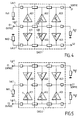
- a distributed double amplifier includes a Lgcl common grid line and two drain lines common Ldcl and Ldc2 to realize an active switch to one input and two outputs (DAD1, figure 4) or includes two lines of common grids Lgcl and Lgc2 and a line of Ldcl common drains to realize an active switch to two inputs and an output (DAD2, figure 5).
- the center line is the line of common grids Lgcl.
- the lower and upper lines are the common drain lines Ldc1 and Ldc2.
- Polarization means are provided for polarize (control) the T transistors of structures AS higher amplifiers (individualized in AS1 to AS3) and below AI (individualized in AI1 to AI3), i.e. amplifier mode, either in blocked mode.
- biasing means are similar to those described with reference to Figure 3.
- the command to switch between blocked mode and the amplifier mode is applied to the grids of T transistors of higher amplifying structures AS and below AI. You can also apply the command switching on drains but this solution is more complex due to the drain current which penalizes the speed of the order.
- a CDE capacity can be connected in series with the capacity of the gate (CGS) of a transistor T to form a bridge capacitive. Such a bridge decreases the gain depending on the frequency. So the gain of each cell can be modulated in absolute amplitude or in amplitude depending on the frequency according to the presence and the value of the CDE capacity between the common gate line and the gate of a transistor. This modulation can be applied to the amplitude on the entire frequency band or a variation of amplitude versus frequency for creation a positive slope in order to compensate for the losses of passive circuits.
- the biasing means are arranged so that when T transistors of higher amplifying structures AS are polarized in a blocked state, the transistors T of lower amplifying structures AI are polarized in an amplifying state, and vice versa.
- the input signal applied to input E1 propagates on the Lgcl common grid line to be absorbed by the load Reg.
- a current is then generated by each transistor of each lower amplifying structure. This current thus generated supplies the Ldc2 common drain line. This current is propagates partly towards the Rd2 load and partly towards the S2 output.
- the components that go to the S2 output are overlap with the same phase, provided that the time of intercell propagation be identical on the line of common drains Ldc2 and on the grid line Lgc1.
- Amplification is then the sum of the amplifications carried out by each transistor of each lower amplifying structure. No current is propagated on the line of drains common Ldcl insofar as the transistors of the structures upper amplifiers are polarized in blocked mode.
- Such a distributed double amplifier DAD1 can be produced using transistors belonging to the PH25 sector of the UMS Foundry (Franco-German company).
- the gain obtained in the frequency band 1 to 20 GHz is around +7 dB for the amplified channel, and of the order of - 20 dB for the channel blocked.
- the behavior of the circuit described with reference to Figure 4 in high signal mode shows an output power greater than 10 dBm with 1 dB of compression for consumption 38 mA on 3 volts, which corresponds to a power consumed less than 120 mW.
- Gain, output power and consumption can be adjusted by varying the number of cells, the size of the transistors T, as well as the number of capacitors CDE.
- the center line is the line of common drains Ldgcl.
- the lower and upper lines are the common grid lines Lgc1 and Lgc2.
- the double amplifier of FIG. 5 comprises means for polarization (not shown) to control the transistors T of the upper AS and lower amplifying structures AI, either in amplifier mode, or in blocked mode, in depending on the value of the input bit of the digital control.
- the biasing means are arranged so that when T transistors of higher amplifying structures AS are polarized in a blocked state, the transistors T of lower amplifying structures AI are polarized in an amplifying state, and vice versa.
- the input signal applied at input E2 propagates on the common grid line Lgc2 to be absorbed by the load Rg2.
- a current is then generated by each transistor of each lower amplifying structure. This current thus generated supplies the common drain line Ldc1. This current is propagates partly towards the load Rd1 and partly towards the output S1.
- the components that go to the SI output are overlap with the same phase, provided that the time of intercell propagation be identical on the line of common drains Ldc1 and on the common grid line Lgc2.
- the amplification is then the sum of the amplifications made by each transistor of each amplifier structure lower. Only the signal propagating on the line of common grid Lgc2 is amplified insofar as the transistors of the higher amplifying structures are polarized in blocked mode.
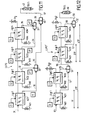
- FIG. 6 there is shown a double DAD1 distributed amplifier, substantially similar to that described with reference to FIG. 4, put in series with a DAD2 dual distributed amplifier, substantially similar to that described with reference to FIG. 5.
- Such a structure makes it possible to produce a device for phase control as described with reference to FIG. 1, in which the dual distributed amplifier DAD1 plays the role of upstream active switch, and in which double DAD2 distributed amplifier acts as a switch active downstream.
- the double distributed amplifier DAD1 of figure 6 includes for example a higher amplifying structure less (the last from the left) compared to the dual distributed amplifier DAD1 of FIG. 4. Such a deletion changes the propagation time of the current on the line of drains Ldc1.
- the double distributed amplifier DAD2 in FIG. 6 includes for example a higher amplifying structure less (the first from the left) by compared to the double distributed amplifier DAD2 of the figure 5.
- a passive RT time delay can be added between the line of Ldc2 drains of the dual distributed amplifier DAD1 and the Lgc2 grid line of the DAD2 distributed double amplifier.
- the upper line constitutes a first track while the lower line constitutes a second way.
- the choice of the control of the transistors makes it possible to make pass the current either according to the first way, or according to the second way.
- the choice of channel can be determined according to the delay temporal to be applied to said current, said delay being function of the number of amplifying structures and the RT delay value.
- amplifying structures represented as a triangle with reference to FIGS. 3 to 6 can comprise one or more transistors, field effect or bipolar type, with or without mounting cascode, with or without CDE capacity in series with capacity of the transistor gate.
- FIG 7 there is shown a simple AD distributed amplifier, conforming to the prior art, according to a variant of schematic representation slightly different from that used in figure 3 and which will be shown in the following figures.
- Reference C designates the digital control means which act on the blocked or amplifier state of the transistors T of the distributed amplifier AD.
- the input E of the distributed amplifier AD is connected to one of the ends of the common grid line Lgc.
- the reference CH designates the load to which the output S of the distributed amplifier AD.
- the load has a value of 50 ohms and the characteristic impedances Zd and Zg respectively of the lines of common drains Ldc and Lgc common grids are 50 ohms.
- the resistances Rg and Rd terminals are 50 ohms.
- r0 is the propagation time of the current along the line of common Lgcl grids, from entrance E to point Rg.
- r is the propagation time of the current of the input E to exit S.
- r - r0 represents approximately the delay time at passage of the active element (transistor) of each of cells (assumed to be identical). To simplify, we can consider that this difference is zero since we will focus below only on relative delays.
- the LAD dual distributed amplifier includes a common grid line 10 formed of two sections of grid lines Lgc1 and Lgc2 put in series and two lines separate drains Ldc1 and Ldc2 to make two circuits switching circuits distributed at one input 12 and two outputs 14 and 16.
- the section of grid line Lgc1 is the grid line common of the AD1 distributed amplifier whose structure is similar to that of a simple distributed amplifier AD described with reference to Figure 7, while the stretch of grid line Lgc2 is the common grid line of AD2 distributed amplifier with a similar structure to that of the simple distributed amplifier AD described in reference to figure 7.
- Input 12 of the LAD dual distributed amplifier is connected at one end of the Lgc1 grid line.
- the other end of the Lgc1 grid line is directly connected (or via passive delay) at one end of the line of Lgc2 grids.
- the other end of the grid line Lgc2 is connected to the terminal resistance Rg.
- Ldc1 line of drains One end of the Ldc1 line of drains is connected to the terminal resistance Rd1. The other end of the line Ldcl drains are connected to a load CH1, via output 14. Likewise, one end of the line of drains Ldc2 is connected to the terminal resistance Rd2. The other end of the line of drains Ldc2 is connected to a load CH2, via the exit 16.
- the impedances of the loads CH1 and CH2 are conventionally of 50 ohms.
- the control of the continuous polarization means C1 of the grids and drains of the amplifier T transistors distributed AD1 and the means of continuous polarizations C2 of grids and drains of the amplifier T transistors distributed AD2 is chosen so that the transistors T of the amplifier AD1 are polarized in passing mode (or amplifier) when the transistors T of the amplifier AD2 are polarized in blocked mode and vice versa.
- the double Figure 8 amplifier is suitable for switching active.
- its structure can also be used to create a line programmable length (delay line).
- FIG. 9 there is shown a quadruple QAD distributed amplifier consisting of two doubles distributed amplifiers LAD1 and LAD2, similar to those described with reference to FIG. 8, and placed in series according to the invention.
- the quadruple distributed amplifier QAD includes a common grid line 20 formed of four sections of grid lines Lgc1 to Lgc4 put in series and four separate drain lines Ldc1 to Ldc4 to realize the equivalent of four switching circuits distributed to an input 22 and four outputs 24, 26, 28, and 30.
- the gain of the double or quadruple amplifier is in the range of +7 to +10 dB in the 1-20 GHz frequency range.
- a programmable length line LLP1 of 1 bit is likely to be achieved using a double distributed amplifier consisting of two amplifiers distributed AD1 and AD2, similar to those described with reference in FIG. 7, placed in series in accordance with FIG. 8, and whose outputs 14 and 16 are connected to a summing member 18, the output 19 of the summing member 18 being connected to a single charge 21, conventionally 50 ohms.
- ⁇ is the propagation time of the current of the input 12 until exit 14.
- 2 ⁇ is the propagation time of the current of the input 12, until exit 16.
- the signal is amplified by stage AD1 and delayed by ⁇ or amplified by stage AD2 and delayed by 2 ⁇ .
- the difference in delay is equal to ⁇ between the two states.
- this difference in level can be compensated by adding an asymmetry between the two stages AD1 and AD2.
- the AD2 stage may have more gain important that the AD1 stage, if necessary with a slope slightly positive depending on the frequency.
- This compensation can also be obtained by adjusting the size transistors and on the passive circuits constituting the lines of grids and drains.
- the CDE capacity mentioned above and put in series with the capacity of the grid transistor also provides a positive gain slope in frequency.
- circuit LLP1 described with reference to Figure 10 performs simultaneously the following four functions: amplification, switching, delay, and gain correction.
- the "high" level of gate voltage associated with the value 1 of the polarization command C can vary, by example depending on the temperature to make a gain correction occurring throughout the circuit.
- each structure distributed thus performs the following functions: amplification, switching, delay, gain correction, and compensation gain.
- the two outputs 14 and 16 into one output 19.
- a wilkinson type bridge can be used as passive summing organ.
- the summing body can also be active type as the summing organ (two inputs and one output) described with reference to Figure 5.
- the amplifying structures distributed offer some choices in impedance lines of drains that are applied to organs summers. We can therefore optimize the choice of organ summator (active or passive) as well as the impedance of the lines drains (50, 100, or 200 ohms).
- a line has been shown 2-bit programmable length LLP2, produced using a quadruple distributed amplifier consisting of two doubles LLP1 distributed amplifiers, similar to those described in reference to FIG. 10, placed in series in accordance with the Figure 10, and whose outputs 30 and 32 are connected to a first summing member 33 and whose outputs 34 and 36 are connected to a second summing member 37, the output 35 of the first summing organ 33, as well as output 39 of the second summing organ being connected to a third summing organ 40 whose output 41 is connected to the single load 42, typically 50 ohms impedance.
- ⁇ is the propagation time of the input current 31 until exit 30.
- 2 ⁇ is the propagation time of the current of the input 31 until exit 32.
- 3 ⁇ is the propagation time of the input current 31 until exit 34.
- 4 ⁇ is the propagation time of the input current 31 until exit 36.
- Line LLP2 of figure 11 corresponds to a chain with delay with 4 links of 1 ⁇ delay each.
- the line with programmable length at 2 bits LLP2 includes two summers 50 and 52 instead of three as in the one described with reference to the figure 10.
- the first two cells AD1 to AD2 are put in series according to the double amplifier of figure 10.
- the outputs of the first two 51, and 53 are connected to a summing member 50 whose output 55 is connected to the input of the third cell AD3.
- the third and fourth AD3 and AD4 cells are placed in series in accordance with double amplifier of figure 10.
- the outputs of third and fourth cells 57 and 59 are connected to a summing member 52 whose output 58 is connected to the load 60 impedance 50 ohms.
- the signal can be delayed by 3 ⁇ , 4 ⁇ , 5 ⁇ or 6 ⁇ , i.e. 4 states, i.e. 2 bits.
- the line LLP2 'in FIG. 12 corresponds to two delay chains connected in series, the first delay chain having 2 links of 1 ⁇ delay each and the second chain delay having 2 links of 2 ⁇ delay each.
- the first four cells AD1 to AD4 are put in series according to the quad amplifier in figure 11.
- the outputs of the first four 72, 74, 76, and 80 are connected to a summing member 70 whose single outlet 79 is connected to the input of the fifth cell AD5.
- the fifth and sixth cells AD5 and AD6 are put in series in accordance to the double amplifier of figure 10.
- the outputs of fifth and sixth cells 82 and 84 are connected to a summing member 80 whose output 86 is connected to the load 88 impedance 50 ohms.
- the signal can be delayed by 5 ⁇ , 6 ⁇ , 7 ⁇ , 8 ⁇ , 9 ⁇ , 10 ⁇ , 11 ⁇ , or 12 ⁇ , i.e. 8 states, i.e. 3 bits.
- line LLP3 in Figure 13 corresponds to two delay chains connected in series, the first delay chain having 4 links of 1 ⁇ delay each and the second chain having 2 links of 4 ⁇ delay each.
- the LLP4 line includes 8 cells with distributed structures single AD1 to AD8.
- the first four cells AD1 to AD4 are connected in series according to the quad amplifier in Figure 11.
- the outputs of the first four cells 102, 104, 106, and 108 are connected to a summing member 100 whose output 109 is connected to the input of the fifth AD5 cell.
- the last four cells AD5 to AD8 are connected in series according to the quadruple amplifier of the figure 11.
- the outputs of the last four first cells 112, 114, 116, and 118 are connected to a summing organ 110 whose output 119 is connected to load 120, of impedance 50 ohms.
- the signal can be delayed by 5 ⁇ , 6 ⁇ , 7 ⁇ , 8 ⁇ , 9 ⁇ , 10 ⁇ , 11 ⁇ , 12 ⁇ , 13 ⁇ , 14 ⁇ , 15 ⁇ , 16 ⁇ , 17 ⁇ , 18 ⁇ , 19 ⁇ , or 20 ⁇ , i.e. 16 states, i.e. 4 bits.
- line LLP4 in Figure 14 corresponds to two delay chains connected in series, the first delay chain having 4 links of 1 ⁇ delay each and the second chain having 4 links of 4 ⁇ delay each.
- the summing members generate band losses or limitations when they are liabilities, or significant consumption when they are assets.
- the Applicant has posed the problem of resolving these problems.
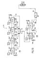
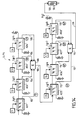
- the present invention provides a solution based on a double amplifier distributed in a so-called configuration "auto-recombinant" in which the drain line plays the role of summator.
- the single line of drains Ldc1 serves here as a summing organ. It collects the amplified signals either from the line of upper grids Lgc1, with a certain delay time, either from the lower grid line Lgc2, or with a delay time substantially double that of the line superior.
- looping a line of grid on the other may itself have a delay; who can be performed on the circuit (chip) or outside. Such a delay increases the difference of delay between the two states and achieve a line bit of programmable length of highest weight.
- the loopback between the end of the Lgc1 line and the start of line Lgc2 includes 3 passive delays RP1 to RP3, of individual value ⁇ to simplify.
- the lower grid line Lgc2 includes a cell additional active compared to the grid line higher Lgc1, to compensate for losses due to cells passive RP1 to RP3 inserted between lines Lgc1 and Lgc2.
- This additional active cell represents a cell passive on the line of drains when the transistors superiors are in amplifier mode.
Landscapes
- Engineering & Computer Science (AREA)
- Power Engineering (AREA)
- Amplifiers (AREA)
- Microwave Amplifiers (AREA)
- Networks Using Active Elements (AREA)
Applications Claiming Priority (2)
| Application Number | Priority Date | Filing Date | Title |
|---|---|---|---|
| FR9816556 | 1998-12-29 | ||
| FR9816556A FR2787949B1 (fr) | 1998-12-29 | 1998-12-29 | Dispositif de controle de phase constitue de multiples structures amplificatrices distribuees a elements actifs commutables |
Publications (2)
| Publication Number | Publication Date |
|---|---|
| EP1017171A1 true EP1017171A1 (de) | 2000-07-05 |
| EP1017171B1 EP1017171B1 (de) | 2007-01-24 |
Family
ID=9534602
Family Applications (1)
| Application Number | Title | Priority Date | Filing Date |
|---|---|---|---|
| EP99403267A Expired - Lifetime EP1017171B1 (de) | 1998-12-29 | 1999-12-23 | Phasensteuervorrichtung mit einer Vielzahl von Kettenverstärkerstrukturen mit schaltbaren aktiven Elementen zur Erstellung einer Übertragungsleitung mit programmierbarer Länge |
Country Status (4)
| Country | Link |
|---|---|
| EP (1) | EP1017171B1 (de) |
| AT (1) | ATE352901T1 (de) |
| DE (1) | DE69934962T2 (de) |
| FR (1) | FR2787949B1 (de) |
Cited By (4)
| Publication number | Priority date | Publication date | Assignee | Title |
|---|---|---|---|---|
| FR2833782A1 (fr) * | 2001-12-18 | 2003-06-20 | Thales Sa | Commutateur actif large bande a deux entrees et deux sorties a structure distribuee, et dispositif de controle de phase comportant un tel commutateur |
| WO2002075921A3 (en) * | 2001-03-15 | 2003-12-11 | Motorola Inc | Distributed amplifier having separately biased sections |
| FR2953665A1 (fr) * | 2009-12-08 | 2011-06-10 | Thales Sa | Amplificateur distribue hyperfrequences large bande et grande dynamique et structures hyperfrequences utilisant un tel amplificateur |
| WO2017180028A1 (en) * | 2016-04-11 | 2017-10-19 | Telefonaktiebolaget Lm Ericsson (Publ) | Modular and scalable power amplifier system |
Citations (2)
| Publication number | Priority date | Publication date | Assignee | Title |
|---|---|---|---|---|
| US4772858A (en) * | 1987-11-04 | 1988-09-20 | Raytheon Company | Distributed amplifying switch/rf combiner |
| US4788509A (en) * | 1986-08-15 | 1988-11-29 | Itt Gallium Arsenide Technology Center, A Division Of Itt Corporation | Phase shifter |
-
1998
- 1998-12-29 FR FR9816556A patent/FR2787949B1/fr not_active Expired - Fee Related
-
1999
- 1999-12-23 EP EP99403267A patent/EP1017171B1/de not_active Expired - Lifetime
- 1999-12-23 AT AT99403267T patent/ATE352901T1/de not_active IP Right Cessation
- 1999-12-23 DE DE69934962T patent/DE69934962T2/de not_active Expired - Lifetime
Patent Citations (2)
| Publication number | Priority date | Publication date | Assignee | Title |
|---|---|---|---|---|
| US4788509A (en) * | 1986-08-15 | 1988-11-29 | Itt Gallium Arsenide Technology Center, A Division Of Itt Corporation | Phase shifter |
| US4772858A (en) * | 1987-11-04 | 1988-09-20 | Raytheon Company | Distributed amplifying switch/rf combiner |
Non-Patent Citations (1)
| Title |
|---|
| MILITARY MICROWAVES CONFERENCE PROCEEDINGS. BRIGHTON, JUNE 24 - 26, 1986., TUNBRIDGE WELLS, MICROWAVE LTD., GB, vol. CONF. 5, 1 January 1986 (1986-01-01), GB, pages 583 - 596., XP002115859 * |
Cited By (7)
| Publication number | Priority date | Publication date | Assignee | Title |
|---|---|---|---|---|
| WO2002075921A3 (en) * | 2001-03-15 | 2003-12-11 | Motorola Inc | Distributed amplifier having separately biased sections |
| FR2833782A1 (fr) * | 2001-12-18 | 2003-06-20 | Thales Sa | Commutateur actif large bande a deux entrees et deux sorties a structure distribuee, et dispositif de controle de phase comportant un tel commutateur |
| EP1326335A1 (de) | 2001-12-18 | 2003-07-09 | Thales | Aktive Breitbandschalter mit verteilter Struktur, zwei Eingänge und zwei Ausgänge, und Vorrichtung zur Phasensteuerung mit solch einem Schalter |
| US6798281B2 (en) | 2001-12-18 | 2004-09-28 | Thales | Two-input/two-output broadband active selector switch with distributed structure, and phase control device comprising such a switch |
| FR2953665A1 (fr) * | 2009-12-08 | 2011-06-10 | Thales Sa | Amplificateur distribue hyperfrequences large bande et grande dynamique et structures hyperfrequences utilisant un tel amplificateur |
| WO2017180028A1 (en) * | 2016-04-11 | 2017-10-19 | Telefonaktiebolaget Lm Ericsson (Publ) | Modular and scalable power amplifier system |
| US10116265B2 (en) | 2016-04-11 | 2018-10-30 | Telefonaktiebolaget Lm Ericsson (Publ) | Modular and scalable power amplifier system |
Also Published As
| Publication number | Publication date |
|---|---|
| DE69934962T2 (de) | 2007-11-15 |
| DE69934962D1 (de) | 2007-03-15 |
| ATE352901T1 (de) | 2007-02-15 |
| FR2787949A1 (fr) | 2000-06-30 |
| FR2787949B1 (fr) | 2001-05-11 |
| EP1017171B1 (de) | 2007-01-24 |
Similar Documents
| Publication | Publication Date | Title |
|---|---|---|
| FR2916108A1 (fr) | Amplificateur de puissance a haute frequence | |
| FR2558997A1 (fr) | Amplificateur correcteur du temps de propagation de groupe de signaux electriques et chaine d'amplification a frequence intermediaire de faisceaux hertziens comportant un tel amplificateur | |
| FR2928793A1 (fr) | Dispositif d'amplification de puissance spatial multi-sources | |
| EP0047690B1 (de) | Mehrere Transistoren enthaltender, monolithischer Verstärker mit Leistungsteilung und Leistungszusammenführung | |
| FR2721156A1 (fr) | Circuit de linéarisation à prédistorsion. | |
| EP0124423B1 (de) | Hyperfrequenter Leistungsverstärker | |
| EP0138637B1 (de) | Schaltmatrix für elektrische Mikrowellensignale | |
| EP2159922B1 (de) | Gesteuerter aktiver Mikrowellen-Duplexer | |
| EP0133080B1 (de) | Frequenzunabhängiger Impedanzanpassungsvierpol und Wanderwellenverstärker der diesen verwendet | |
| EP1017171B1 (de) | Phasensteuervorrichtung mit einer Vielzahl von Kettenverstärkerstrukturen mit schaltbaren aktiven Elementen zur Erstellung einer Übertragungsleitung mit programmierbarer Länge | |
| EP0596568B1 (de) | Halbleitervorrichtung mit einer monolithisch integrierten Kettenverstärkerschaltung mit grosser Bandbreite und hohem Verstärkungsgrad | |
| FR2595173A1 (fr) | Circuit amplificateur distribue large bande dans le domaine des hyperfrequences | |
| FR2625052A1 (fr) | Circuit hyperfrequences comprenant au moins un transistor a effet de champ charge | |
| CA2060720C (fr) | Dephaseur variable analogique pour signaux hyperfrequence | |
| EP1326335A1 (de) | Aktive Breitbandschalter mit verteilter Struktur, zwei Eingänge und zwei Ausgänge, und Vorrichtung zur Phasensteuerung mit solch einem Schalter | |
| EP2182631A2 (de) | Mikrowellen-Breitband-Verstärkerzelle mit regelbarer Verstärkung und eine solche Zelle umfassender Verstärker | |
| FR2633119A1 (fr) | Circuit actif hyperfrequences du type passe-tout | |
| FR2747523A1 (fr) | Amplificateur distribue adaptateur basse impedance pour emetteur optoelectronique de signaux hyperfrequences a tres large bande | |
| FR2604574A1 (fr) | Amplificateur a transistors a effet de champ a constantes reparties et son alimentation de tension de polarisation | |
| WO2008003751A1 (fr) | Dispositif d'amplification d'un signal hyperfrequence a large bande | |
| EP3235125A1 (de) | Verbesserter verstärkerkanal wie etwa eine gain-block-vorrichtung | |
| FR2750546A1 (fr) | Amplificateur passe-tout pour signaux hyperfrequences | |
| FR2955220A1 (fr) | Filtre actif a bande passante modulable | |
| FR2953665A1 (fr) | Amplificateur distribue hyperfrequences large bande et grande dynamique et structures hyperfrequences utilisant un tel amplificateur | |
| FR2955721A1 (fr) | Cellule amplificatrice hyperfrequence large bande a gain reglable faible cout et amplificateur distribue comportant une telle cellule |
Legal Events
| Date | Code | Title | Description |
|---|---|---|---|
| PUAI | Public reference made under article 153(3) epc to a published international application that has entered the european phase |
Free format text: ORIGINAL CODE: 0009012 |
|
| AK | Designated contracting states |
Kind code of ref document: A1 Designated state(s): AT BE CH CY DE DK ES FI FR GB GR IE IT LI LU MC NL PT SE |
|
| AX | Request for extension of the european patent |
Free format text: AL;LT;LV;MK;RO;SI |
|
| 17P | Request for examination filed |
Effective date: 20001220 |
|
| AKX | Designation fees paid |
Free format text: AT BE CH CY DE DK ES FI FR GB GR IE IT LI LU MC NL PT SE |
|
| GRAP | Despatch of communication of intention to grant a patent |
Free format text: ORIGINAL CODE: EPIDOSNIGR1 |
|
| GRAS | Grant fee paid |
Free format text: ORIGINAL CODE: EPIDOSNIGR3 |
|
| RAP1 | Party data changed (applicant data changed or rights of an application transferred) |
Owner name: THALES SYSTEMES AEROPORTES S.A. |
|
| GRAA | (expected) grant |
Free format text: ORIGINAL CODE: 0009210 |
|
| AK | Designated contracting states |
Kind code of ref document: B1 Designated state(s): AT BE CH CY DE DK ES FI FR GB GR IE IT LI LU MC NL PT SE |
|
| PG25 | Lapsed in a contracting state [announced via postgrant information from national office to epo] |
Ref country code: NL Free format text: LAPSE BECAUSE OF FAILURE TO SUBMIT A TRANSLATION OF THE DESCRIPTION OR TO PAY THE FEE WITHIN THE PRESCRIBED TIME-LIMIT Effective date: 20070124 Ref country code: IE Free format text: LAPSE BECAUSE OF FAILURE TO SUBMIT A TRANSLATION OF THE DESCRIPTION OR TO PAY THE FEE WITHIN THE PRESCRIBED TIME-LIMIT Effective date: 20070124 Ref country code: FI Free format text: LAPSE BECAUSE OF FAILURE TO SUBMIT A TRANSLATION OF THE DESCRIPTION OR TO PAY THE FEE WITHIN THE PRESCRIBED TIME-LIMIT Effective date: 20070124 Ref country code: DK Free format text: LAPSE BECAUSE OF FAILURE TO SUBMIT A TRANSLATION OF THE DESCRIPTION OR TO PAY THE FEE WITHIN THE PRESCRIBED TIME-LIMIT Effective date: 20070124 Ref country code: AT Free format text: LAPSE BECAUSE OF FAILURE TO SUBMIT A TRANSLATION OF THE DESCRIPTION OR TO PAY THE FEE WITHIN THE PRESCRIBED TIME-LIMIT Effective date: 20070124 |
|
| REG | Reference to a national code |
Ref country code: GB Ref legal event code: FG4D Free format text: NOT ENGLISH |
|
| REG | Reference to a national code |
Ref country code: CH Ref legal event code: EP |
|
| REG | Reference to a national code |
Ref country code: IE Ref legal event code: FG4D Free format text: LANGUAGE OF EP DOCUMENT: FRENCH |
|
| REF | Corresponds to: |
Ref document number: 69934962 Country of ref document: DE Date of ref document: 20070315 Kind code of ref document: P |
|
| PG25 | Lapsed in a contracting state [announced via postgrant information from national office to epo] |
Ref country code: SE Free format text: LAPSE BECAUSE OF FAILURE TO SUBMIT A TRANSLATION OF THE DESCRIPTION OR TO PAY THE FEE WITHIN THE PRESCRIBED TIME-LIMIT Effective date: 20070424 |
|
| PG25 | Lapsed in a contracting state [announced via postgrant information from national office to epo] |
Ref country code: ES Free format text: LAPSE BECAUSE OF FAILURE TO SUBMIT A TRANSLATION OF THE DESCRIPTION OR TO PAY THE FEE WITHIN THE PRESCRIBED TIME-LIMIT Effective date: 20070505 |
|
| GBT | Gb: translation of ep patent filed (gb section 77(6)(a)/1977) |
Effective date: 20070424 |
|
| PG25 | Lapsed in a contracting state [announced via postgrant information from national office to epo] |
Ref country code: PT Free format text: LAPSE BECAUSE OF FAILURE TO SUBMIT A TRANSLATION OF THE DESCRIPTION OR TO PAY THE FEE WITHIN THE PRESCRIBED TIME-LIMIT Effective date: 20070625 |
|
| NLV1 | Nl: lapsed or annulled due to failure to fulfill the requirements of art. 29p and 29m of the patents act | ||
| REG | Reference to a national code |
Ref country code: IE Ref legal event code: FD4D |
|
| PLBE | No opposition filed within time limit |
Free format text: ORIGINAL CODE: 0009261 |
|
| STAA | Information on the status of an ep patent application or granted ep patent |
Free format text: STATUS: NO OPPOSITION FILED WITHIN TIME LIMIT |
|
| 26N | No opposition filed |
Effective date: 20071025 |
|
| PG25 | Lapsed in a contracting state [announced via postgrant information from national office to epo] |
Ref country code: GR Free format text: LAPSE BECAUSE OF FAILURE TO SUBMIT A TRANSLATION OF THE DESCRIPTION OR TO PAY THE FEE WITHIN THE PRESCRIBED TIME-LIMIT Effective date: 20070425 |
|
| BERE | Be: lapsed |
Owner name: THALES SYSTEMES AEROPORTES S.A. Effective date: 20071231 |
|
| PG25 | Lapsed in a contracting state [announced via postgrant information from national office to epo] |
Ref country code: MC Free format text: LAPSE BECAUSE OF NON-PAYMENT OF DUE FEES Effective date: 20071231 |
|
| REG | Reference to a national code |
Ref country code: CH Ref legal event code: PL |
|
| PG25 | Lapsed in a contracting state [announced via postgrant information from national office to epo] |
Ref country code: BE Free format text: LAPSE BECAUSE OF NON-PAYMENT OF DUE FEES Effective date: 20071231 |
|
| PG25 | Lapsed in a contracting state [announced via postgrant information from national office to epo] |
Ref country code: LI Free format text: LAPSE BECAUSE OF NON-PAYMENT OF DUE FEES Effective date: 20071231 Ref country code: CH Free format text: LAPSE BECAUSE OF NON-PAYMENT OF DUE FEES Effective date: 20071231 |
|
| REG | Reference to a national code |
Ref country code: FR Ref legal event code: ST Effective date: 20081020 |
|
| PG25 | Lapsed in a contracting state [announced via postgrant information from national office to epo] |
Ref country code: FR Free format text: LAPSE BECAUSE OF NON-PAYMENT OF DUE FEES Effective date: 20071231 |
|
| PG25 | Lapsed in a contracting state [announced via postgrant information from national office to epo] |
Ref country code: CY Free format text: LAPSE BECAUSE OF FAILURE TO SUBMIT A TRANSLATION OF THE DESCRIPTION OR TO PAY THE FEE WITHIN THE PRESCRIBED TIME-LIMIT Effective date: 20070124 |
|
| PG25 | Lapsed in a contracting state [announced via postgrant information from national office to epo] |
Ref country code: LU Free format text: LAPSE BECAUSE OF NON-PAYMENT OF DUE FEES Effective date: 20071223 |
|
| PGFP | Annual fee paid to national office [announced via postgrant information from national office to epo] |
Ref country code: IT Payment date: 20101224 Year of fee payment: 12 Ref country code: GB Payment date: 20101222 Year of fee payment: 12 |
|
| PGFP | Annual fee paid to national office [announced via postgrant information from national office to epo] |
Ref country code: DE Payment date: 20101215 Year of fee payment: 12 |
|
| GBPC | Gb: european patent ceased through non-payment of renewal fee |
Effective date: 20111223 |
|
| REG | Reference to a national code |
Ref country code: DE Ref legal event code: R119 Ref document number: 69934962 Country of ref document: DE Effective date: 20120703 |
|
| PG25 | Lapsed in a contracting state [announced via postgrant information from national office to epo] |
Ref country code: DE Free format text: LAPSE BECAUSE OF NON-PAYMENT OF DUE FEES Effective date: 20120703 Ref country code: GB Free format text: LAPSE BECAUSE OF NON-PAYMENT OF DUE FEES Effective date: 20111223 |
|
| PG25 | Lapsed in a contracting state [announced via postgrant information from national office to epo] |
Ref country code: IT Free format text: LAPSE BECAUSE OF NON-PAYMENT OF DUE FEES Effective date: 20111223 |