EP1017174B1 - Circuit et procédé de mise en oeuvre d'une logique séquentielle autonome - Google Patents
Circuit et procédé de mise en oeuvre d'une logique séquentielle autonome Download PDFInfo
- Publication number
- EP1017174B1 EP1017174B1 EP19990480085 EP99480085A EP1017174B1 EP 1017174 B1 EP1017174 B1 EP 1017174B1 EP 19990480085 EP19990480085 EP 19990480085 EP 99480085 A EP99480085 A EP 99480085A EP 1017174 B1 EP1017174 B1 EP 1017174B1
- Authority
- EP
- European Patent Office
- Prior art keywords
- mode
- logic
- dummy
- input
- logic circuits
- Prior art date
- Legal status (The legal status is an assumption and is not a legal conclusion. Google has not performed a legal analysis and makes no representation as to the accuracy of the status listed.)
- Expired - Lifetime
Links
- 238000000034 method Methods 0.000 title claims description 11
- 230000001902 propagating effect Effects 0.000 claims description 3
- 238000012544 monitoring process Methods 0.000 claims 1
- 238000013461 design Methods 0.000 description 12
- 238000013459 approach Methods 0.000 description 8
- 230000007704 transition Effects 0.000 description 7
- 230000001934 delay Effects 0.000 description 4
- 230000009977 dual effect Effects 0.000 description 4
- 230000001360 synchronised effect Effects 0.000 description 4
- 238000012546 transfer Methods 0.000 description 4
- XUIMIQQOPSSXEZ-UHFFFAOYSA-N Silicon Chemical compound [Si] XUIMIQQOPSSXEZ-UHFFFAOYSA-N 0.000 description 3
- 238000004519 manufacturing process Methods 0.000 description 3
- 230000008859 change Effects 0.000 description 2
- 230000000694 effects Effects 0.000 description 2
- 238000005516 engineering process Methods 0.000 description 2
- 230000007613 environmental effect Effects 0.000 description 2
- 230000003071 parasitic effect Effects 0.000 description 2
- 230000008569 process Effects 0.000 description 2
- 229910052710 silicon Inorganic materials 0.000 description 2
- 239000010703 silicon Substances 0.000 description 2
- RYGMFSIKBFXOCR-UHFFFAOYSA-N Copper Chemical compound [Cu] RYGMFSIKBFXOCR-UHFFFAOYSA-N 0.000 description 1
- 206010019233 Headaches Diseases 0.000 description 1
- XAGFODPZIPBFFR-UHFFFAOYSA-N aluminium Chemical compound [Al] XAGFODPZIPBFFR-UHFFFAOYSA-N 0.000 description 1
- 229910052782 aluminium Inorganic materials 0.000 description 1
- 230000005540 biological transmission Effects 0.000 description 1
- 239000003990 capacitor Substances 0.000 description 1
- 229910052802 copper Inorganic materials 0.000 description 1
- 239000010949 copper Substances 0.000 description 1
- 230000007547 defect Effects 0.000 description 1
- 230000001419 dependent effect Effects 0.000 description 1
- 238000012938 design process Methods 0.000 description 1
- 230000001627 detrimental effect Effects 0.000 description 1
- 238000009826 distribution Methods 0.000 description 1
- 231100000869 headache Toxicity 0.000 description 1
- 230000036039 immunity Effects 0.000 description 1
- 230000010354 integration Effects 0.000 description 1
- 239000000463 material Substances 0.000 description 1
- 238000004806 packaging method and process Methods 0.000 description 1
- 238000012545 processing Methods 0.000 description 1
- 230000000644 propagated effect Effects 0.000 description 1
- 230000009291 secondary effect Effects 0.000 description 1
- 239000004065 semiconductor Substances 0.000 description 1
- 238000010561 standard procedure Methods 0.000 description 1
- 238000003860 storage Methods 0.000 description 1
- 230000002459 sustained effect Effects 0.000 description 1
Images



Classifications
-
- H—ELECTRICITY
- H03—ELECTRONIC CIRCUITRY
- H03K—PULSE TECHNIQUE
- H03K19/00—Logic circuits, i.e. having at least two inputs acting on one output; Inverting circuits
- H03K19/02—Logic circuits, i.e. having at least two inputs acting on one output; Inverting circuits using specified components
- H03K19/08—Logic circuits, i.e. having at least two inputs acting on one output; Inverting circuits using specified components using semiconductor devices
- H03K19/094—Logic circuits, i.e. having at least two inputs acting on one output; Inverting circuits using specified components using semiconductor devices using field-effect transistors
- H03K19/096—Synchronous circuits, i.e. using clock signals
-
- H—ELECTRICITY
- H03—ELECTRONIC CIRCUITRY
- H03K—PULSE TECHNIQUE
- H03K19/00—Logic circuits, i.e. having at least two inputs acting on one output; Inverting circuits
- H03K19/02—Logic circuits, i.e. having at least two inputs acting on one output; Inverting circuits using specified components
- H03K19/173—Logic circuits, i.e. having at least two inputs acting on one output; Inverting circuits using specified components using elementary logic circuits as components
- H03K19/1733—Controllable logic circuits
Definitions
- the present invention relates generally to data processing units and more particularly to a circuit and methods for implementing sequential logic functions from autonomous, i.e., clock-less, self-validating circuits.
- latch outputs are possible inputs to all other cones of logic (recursive feeding is possible and is a common practice especially, when a particular state must be maintained for several cycles of the clock) so as every cone input is stable for a complete clock cycle since every latch is holding its binary information for one clock cycle.
- state of the logic may only change with the clock and any logic function built according to these principles is orderly evolving since it is under the control of a common timing device.
- checking programs have been designed which scrub all the possible paths, pinpointing the ones for which delays are exceeding the period of the clock even though some may not be functional! Then, it is up to the designer to decide if those paths are indeed functional and must be corrected through another round of physical design. This is a time consuming, expensive in terms of computing resources and cumbersome job that is not always successful if the clock period is too tight for the current technology available and the logic function too complex. A dead-end situation that may become obvious only long after the physical design process has started and that may require drastic actions like restarting from scratch with a brand new approach.
- the clock distribution structure exhibits no skew between its various branches over the whole area covered by a logic function implemented on a semiconductor chip (most of the time silicon) or at least has a skew which is lower than the best case of the shortest path present on the chip so as it is not possible to experience any short-cut that would result of a latch feeding another one too soon because their respective clocks are enough skewed to allow propagation to occur on the same master clock transition.
- GA Gate Array
- FPGA Field Programmable Gate Array
- Still another problem of clocked designs is that everything is changing on the advent of a clock transition common to every latch that triggers peaks of current through the power supply terminals of the chips and modules thus, disturbing, among other things, the ground and which may jeopardize the noise immunity of the gates and latches if not contained through a careful design of the packaging at each level, i.e., chip, module and board so as to keep the parasitic inductances as low as possible.
- the light is traveling, in a perfect medium, 30 cm within a time period of 1 nanosecond, which corresponds to the clock period of the current laboratory parts while microprocessor chips are commonly square of 1.5x1.5 cm.
- the speed limitation on the wires has become the limiting factor to increase the performance forcing the manufacturers to use very sophisticated technologies, very expensive in terms of investments, with many wiring layers (5 is becoming the standard) so as to shorten the distances and/or using materials of better electrical characteristics (copper is replacing aluminum although it was very difficult to accommodate its very undesirable secondary effects on silicium) in an attempt to reduce transmission delays.
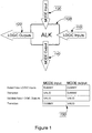
- a logic circuit is disclosed that is operable in a DUMMY mode and in a VALID mode. It comprises a plurality of LOGIC input and output lines each having an asserted and a de-asserted state. It also comprises a plurality of MODE input lines, for turning the logic circuit into the herein above DUMMY or VALID modes along with a plurality of MODE output lines, for detecting whether the logic circuit is operating in the DUMMY or VALID mode. Logic operations are performed between the LOGIC input lines and the LOGIC output lines whenever the VALID mode is active while the DUMMY mode is permitted to propagate throughout the logic circuit regardless of whether the LOGIC input lines are in an asserted or a de-asserted state.
- the logic circuit further comprises a MODE Control for turning the logic circuit into either one of the two herein above modes also, including a PACE signal that, when asserted, turns said logic circuit into the DUMMY mode and an input for a FEEDBACK signal for toggling between the VALID mode and the DUMMY mode when the PACE signal is not asserted along with an output for a FEEDFORWARD signal for reporting what mode controlling means is currently asserting.
- a MODE Control for turning the logic circuit into either one of the two herein above modes also, including a PACE signal that, when asserted, turns said logic circuit into the DUMMY mode and an input for a FEEDBACK signal for toggling between the VALID mode and the DUMMY mode when the PACE signal is not asserted along with an output for a FEEDFORWARD signal for reporting what mode controlling means is currently asserting.
- the logic circuit still comprises a MODE Detect for detecting in which one of the two herein above modes the logic circuit is operating, including an input for the FEEDFORWARD signal just described and an output for the FEEDBACK signal reporting if the detecting means is currently detecting the VALID or the DUMMY mode along with a STATUS for generating a first signal for requesting the assertion of new states on the LOGIC inputs and a second signal for indicating that new states are ready to be used on the LOGIC outputs.
- a MODE Detect for detecting in which one of the two herein above modes the logic circuit is operating, including an input for the FEEDFORWARD signal just described and an output for the FEEDBACK signal reporting if the detecting means is currently detecting the VALID or the DUMMY mode along with a STATUS for generating a first signal for requesting the assertion of new states on the LOGIC inputs and a second signal for indicating that new states are ready to be used on the LOGIC outputs
- circuit and methods of the invention permit to carry out sequential logic functions that do not require a common clock be distributed over a complete function, such as an ASIC or a Processor, to inter-operate.
Landscapes
- Engineering & Computer Science (AREA)
- Physics & Mathematics (AREA)
- Computer Hardware Design (AREA)
- Computing Systems (AREA)
- General Engineering & Computer Science (AREA)
- Mathematical Physics (AREA)
- Power Engineering (AREA)
- Logic Circuits (AREA)
Claims (10)
- Un circuit logique [200], susceptible de fonctionner en mode FICTIF (DUMMY) [260] et en mode VALIDE [270], ledit circuit comprenant :• au moins une ligne d'entrée LOGIQUE [225], chaque ligne d'entrée LOGIQUE ayant un état affirmé et un état désaffirmé ;• au moins une ligne de sortie LOGIQUE [250], chacune desdites lignes de sortie LOGIQUE ayant un état affirmé et un état désaffirmé ;• des moyens d'opération logique [220], pour accomplir des opérations logiques entre lesdites lignes d'entrée LOGIQUE [225] et lesdites lignes de sortie LOGIQUE [250], lorsque ledit mode VALIDE est actif, lesdits moyens d'opérations logiques [220] ayant une entrée de MODE, pour au moins une ligne de commande de MODE [215], et une sortie de MODE, pour au moins une ligne de détection de MODE [230] .• des moyens de propagation de mode, pour propager ledit mode FICTIF à partir de ladite entrée de MODE, par lesdits moyens d'opérations logiques [220], vers ladite sortie de MODE, indépendamment du fait que lesdites lignes d'entrée LOGIQUE [225] soient en un état affirmé ou un état désaffirmé ;• des moyens de commande de mode [210] pour commander un MODE pour ledit circuit logique [200], en faisant passer ledit circuit logique audit mode VALIDE ou audit mode FICTIF, lesdits moyens de commande de mode comprenant :• un moyen d'entrée pour un signal de RYTHME (PACE) [255], capable de forcer ledit mode FICTIF pour ledit circuit logique une fois affirmé ;• un moyen d'entrée pour un signal de RETROACTION (FEEDBACK) [225], pour basculer entre ledit mode VALIDE et ledit mode FICTIF lorsque ledit signal de RYTHME n'est pas affirmé ;• un moyen de sortie pour un signal de REACTION ANTICIPATIVE (FEEDFORWARD) [240], pour faire rapport si lesdits moyens de commande de mode [210] affirment que l'on est audit mode VALIDE, ou audit mode FICTIF ;• un moyen de sortie pour ladite au moins une ligne de commande de mode [215], pour faire passer ledit circuit logique [200] audit mode FICTIF ou audit mode VALIDE ;• des moyens de détection de mode [235] pour détecter le MODE dudit circuit logique, lesdits moyens de détection de mode comprenant :• un moyen d'entrée pour ledit signal de REACTION ANTICIPATIVE [240], afin de surveiller ledit mode des moyens de commande de mode [210] ;• un moyen d'entrée, pour ladite au moins une ligne de détection de MODE [230], pour détecter si ledit circuit [200] fonctionne audit mode FICTIF ou audit mode VALIDE ;• un moyen de sortie pour ledit signal de RETROACTION [255], pour faire rapport desdits moyens de détection de mode [235] ;• un moyen ETAT (STATUS) [245] pour générer un premier signal [373], pour demander l'affirmation de nouveaux états sur lesdites entrées LOGIQUE [225], et un deuxième signal [374], pour indiquer que de nouveaux états sont prêts à être utilisés sur lesdites sorties LOGIQUE [250].
- Un système comprenant une pluralité de circuits logiques selon la revendication 1, comprenant en outre des moyens pour synchroniser en série lesdits circuits logiques, lesdits moyens de synchronisation en série comprenant :• des moyens pour connexion [401] de la sortie RETROACTION, desdits moyens de détection de mode [235] d'un premier [401] de ladite pluralité de circuits logiques, à l'entrée RETROACTION desdits moyens de commande de mode [210] d'un dernier [420] de ladite pluralité de circuits logiques ;• des moyens de connexion [411] [421] de la sortie RETROACTION de chaque moyen de détection de mode [235], en commençant à partir du dernier [420] parmi ladite pluralité de circuits logiques, à l'entrée RETROACTION desdits moyens de commande de mode [210] d'un suivant [410] parmi ladite pluralité de circuits logiques jusqu'au premier [400] de ladite pluralité de circuits logiques ;• des moyens de connexion [422] de la sortie FEEDFORWARD desdits moyens de commande de mode [210] du dernier [420] de ladite pluralité de circuits logiques à l'entrée FEEDFORWARD desdits moyens de détection de mode [235] du premier [400] de ladite pluralité de circuits logiques.
- Un système comprenant une pluralité de circuits logiques selon la revendication 1, comprenant en outre des moyens pour synchroniser en parallèle lesdits circuits logiques, lesdits moyens de synchronisation en parallèle comprenant :• des moyens pour accomplir une opération logique ET sur la totalité des signaux de sortie RETROACTION [501] [502] [503] desdits moyens de détection de mode [235] parmi la totalité de ladite pluralité de circuits logiques ;• des moyens de connexion [510] du résultat de ladite opération logique ET à l'entrée RETROACTION desdits moyens de commande de mode [210] à la totalité de ladite pluralité de circuits logiques ;• des moyens pour utilisation des moyens d'ETAT du circuit logique le plus lent parmi ladite pluralité de circuits logiques, en tant que moyens d'ETAT communs.
- Le système selon la revendication 3, dans lequel les moyens d'ETAT communs à utiliser sont sélectionnés par accomplissement d'une opération logique ET sur les signaux de tous lesdits moyens d'ETAT.
- Le système selon l'une quelconque des revendications 2 à 4, combinant une synchronisation en série et en parallèle.
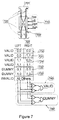
- Un système comprenant une pluralité de circuits selon la revendication 1, comprenant en outre des moyens pour accomplir le mode VALIDE et le mode FICTIF desdits circuits logiques, lesdits moyens comprenant :• des moyens pour définir des états VALIDES [731] et des états FICTIFS [732] sur deux rails d'un dispositif logique à rail dual [700],• des moyens pour coder chacun desdits deux rails avec une pluralité d'états possibles ;• des moyens pour définir une pluralité d'états VALIDES [731] parmi ladite pluralité d'états possibles, sur les deux rails ;• des moyens pour définir un ou une pluralité d'états FICTIFS [732] parmi ladite pluralité d'états possibles, sur les deux rails ;• des moyens pour définir un ou une pluralité d'états VALIDES [734] parmi ladite pluralité d'états VALIDES, sur chaque dit rail individuel ;• des moyens pour définir l'un d'une pluralité d'états FICTIFS [733] parmi ladite pluralité d'états FICTIFS, sur chaque dit rail individuel ;• des moyens de décodage [740] d'un quelconque desdits états VALIDES lorsque les deux rails sont tous deux audit état VALIDE ;• des moyens de décodage [750] d'un quelconque desdits états FICTIFS lorsque les deux rails sont tous deux audit état FICTIF.
- Un procédé de synchronisation en série d'une pluralité de circuits logiques selon la revendication 1, caractérisé en ce qu'il comprend les étapes consistant à :• connecter [401] la sortie RETROACTION desdits moyens de détection de mode [235], d'un premier [401] parmi ladite pluralité de circuits logiques, à l'entrée RETROACTION desdits moyens de commande de mode [210], d'un dernier [420] de ladite pluralité de circuits logiques ;• connecter [411] [421] la sortie RETROACTION de chacun desdits moyens de détection de mode [235] en commençant par le dernier [420] de ladite pluralité de circuits logiques à l'entrée RETROACTION desdits moyens de commande de mode [210] d'un circuit suivant [410] parmi ladite pluralité de circuits logiques, jusqu'au premier [400] de ladite pluralité de circuits logiques ;• connecter [422] la sortie FEEDFORWARD desdits moyens de commande de mode [210] du dernier [420] de ladite pluralité de circuits logiques à l'entrée FEEDFORWARD desdits moyens de détection de mode [235] du premier [400] de ladite pluralité de circuits logiques.
- Un procédé de synchronisation en parallèle d'une pluralité de circuits logiques, selon la revendication 1, caractérisé en ce qu'il comprend les étapes consistant à :• accomplir une opération logique ET sur la totalité des signaux de sortie RETROACTION [501] [502] [503] desdits moyens de détection de mode [235] à partir de la totalité de ladite pluralité de circuits logiques ;• connecter [510] le résultat de ladite opération logique ET à l'entrée RETROACTION desdits moyens de commande de mode [210] à la totalité de ladite pluralité de circuits logiques ;• utiliser les moyens d'ETAT du circuit logique le plus lent parmi ladite pluralité de circuits logiques, en tant que moyens d'ETAT communs.
- Le procédé selon la revendication 8, dans lequel les moyens d'ETAT communs devant être utilisés sont sélectionnés par accomplissement d'une opération logique ET sur les signaux de la totalité desdits moyens d'ETAT.
- Le procédé selon l'une quelconque des revendications 7 à 9, combinant une synchronisation en série et en parallèle.
Priority Applications (1)
| Application Number | Priority Date | Filing Date | Title |
|---|---|---|---|
| EP19990480085 EP1017174B1 (fr) | 1998-12-29 | 1999-09-23 | Circuit et procédé de mise en oeuvre d'une logique séquentielle autonome |
Applications Claiming Priority (3)
| Application Number | Priority Date | Filing Date | Title |
|---|---|---|---|
| EP98480106 | 1998-12-29 | ||
| EP98480106 | 1998-12-29 | ||
| EP19990480085 EP1017174B1 (fr) | 1998-12-29 | 1999-09-23 | Circuit et procédé de mise en oeuvre d'une logique séquentielle autonome |
Publications (2)
| Publication Number | Publication Date |
|---|---|
| EP1017174A1 EP1017174A1 (fr) | 2000-07-05 |
| EP1017174B1 true EP1017174B1 (fr) | 2006-06-14 |
Family
ID=26151827
Family Applications (1)
| Application Number | Title | Priority Date | Filing Date |
|---|---|---|---|
| EP19990480085 Expired - Lifetime EP1017174B1 (fr) | 1998-12-29 | 1999-09-23 | Circuit et procédé de mise en oeuvre d'une logique séquentielle autonome |
Country Status (1)
| Country | Link |
|---|---|
| EP (1) | EP1017174B1 (fr) |
Family Cites Families (7)
| Publication number | Priority date | Publication date | Assignee | Title |
|---|---|---|---|---|
| US5237701A (en) * | 1989-03-31 | 1993-08-17 | Ampex Systems Corporation | Data unpacker using a pack ratio control signal for unpacked parallel fixed m-bit width into parallel variable n-bit width word |
| US5289403A (en) * | 1991-07-08 | 1994-02-22 | Hewlett-Packard Company | Self-timed content addressable memory access mechanism with built-in margin test feature |
| US5387825A (en) * | 1992-08-20 | 1995-02-07 | Texas Instruments Incorporated | Glitch-eliminator circuit |
| JPH06334513A (ja) * | 1993-05-13 | 1994-12-02 | Intel Corp | データ処理装置 |
| US5394407A (en) * | 1993-07-01 | 1995-02-28 | Motorola, Inc. | Method of transferring error correcting code and circuit therefor |
| CA2145361C (fr) * | 1994-03-24 | 1999-09-07 | Martin William Sotheran | Gestionnaire de tampons |
| US5565798A (en) * | 1995-08-21 | 1996-10-15 | International Business Machines Corporation | Self-timed control circuit for self-resetting logic circuitry |
-
1999
- 1999-09-23 EP EP19990480085 patent/EP1017174B1/fr not_active Expired - Lifetime
Also Published As
| Publication number | Publication date |
|---|---|
| EP1017174A1 (fr) | 2000-07-05 |
Similar Documents
| Publication | Publication Date | Title |
|---|---|---|
| US6147539A (en) | Method and structure for improving power consumption on a component while maintaining high operating frequency | |
| Tam et al. | Clock generation and distribution for the first IA-64 microprocessor | |
| JP3331968B2 (ja) | グリッチ分析と低減に重点をおいたレジスタトランスファレベルの電力消費最適化回路、方法、及び記録媒体 | |
| US8484523B2 (en) | Sequential digital circuitry with test scan | |
| Oklobdzija | Clocking and clocked storage elements in a multi-gigahertz environment | |
| US7284143B2 (en) | System and method for reducing clock skew | |
| US6651230B2 (en) | Method for reducing design effect of wearout mechanisms on signal skew in integrated circuit design | |
| US6791355B2 (en) | Spare cell architecture for fixing design errors in manufactured integrated circuits | |
| CN106452394A (zh) | 一种具有自动复位功能的时钟切换结构 | |
| US10354706B1 (en) | Delaying start of user design execution | |
| US6071003A (en) | Method and apparatus for locating critical speed paths in integrated circuits using a clock driver circuit with variable delay | |
| JP2002055732A (ja) | デスキュー回路を有するクロック生成器 | |
| Sawkar et al. | Multi-way partitioning for minimum delay for look-up table based FPGAs | |
| KR20050099714A (ko) | 고집적 저전력 글리치리스 클럭 선택회로 및 이를구비하는 디지털 프로세싱 시스템 | |
| Ferringer et al. | VLSI implementation of a fault-tolerant distributed clock generation | |
| US6515504B1 (en) | Circuits and method for implementing autonomous sequential logic | |
| EP1017174B1 (fr) | Circuit et procédé de mise en oeuvre d'une logique séquentielle autonome | |
| US20040119496A1 (en) | Implementation of multiple flip flops as a standard cell using novel clock generation scheme | |
| US8166438B2 (en) | Low RC local clock distribution | |
| Santhanam et al. | Generic methodolgy and solution for Additive Jitter correction in Mesh based clock architectures | |
| Singh et al. | Self-timed regenerators for high-speed and low-power on-chip global interconnect | |
| Sherrill et al. | Reducing power consumption in asynchronous MTNCL circuits through selective sleep | |
| Lai et al. | Connectivity-Agnostic Built-In Self-Repair of Interconnects in a Chiplet IC | |
| Eedupuganti et al. | High Performance and Power-Aware Scan Flip-Flop Design | |
| US6400188B1 (en) | Test mode clock multiplication |
Legal Events
| Date | Code | Title | Description |
|---|---|---|---|
| PUAI | Public reference made under article 153(3) epc to a published international application that has entered the european phase |
Free format text: ORIGINAL CODE: 0009012 |
|
| AK | Designated contracting states |
Kind code of ref document: A1 Designated state(s): AT BE CH CY DE DK ES FI FR GB GR IE IT LI LU MC NL PT SE |
|
| AX | Request for extension of the european patent |
Free format text: AL;LT;LV;MK;RO;SI |
|
| 17P | Request for examination filed |
Effective date: 20000617 |
|
| AKX | Designation fees paid |
Free format text: AT BE CH CY DE DK ES FI FR GB GR IE IT LI LU MC NL PT SE |
|
| 17Q | First examination report despatched |
Effective date: 20030211 |
|
| GRAP | Despatch of communication of intention to grant a patent |
Free format text: ORIGINAL CODE: EPIDOSNIGR1 |
|
| GRAS | Grant fee paid |
Free format text: ORIGINAL CODE: EPIDOSNIGR3 |
|
| GRAA | (expected) grant |
Free format text: ORIGINAL CODE: 0009210 |
|
| AK | Designated contracting states |
Kind code of ref document: B1 Designated state(s): AT BE CH CY DE DK ES FI FR GB GR IE IT LI LU MC NL PT SE |
|
| PG25 | Lapsed in a contracting state [announced via postgrant information from national office to epo] |
Ref country code: NL Free format text: LAPSE BECAUSE OF FAILURE TO SUBMIT A TRANSLATION OF THE DESCRIPTION OR TO PAY THE FEE WITHIN THE PRESCRIBED TIME-LIMIT Effective date: 20060614 Ref country code: LI Free format text: LAPSE BECAUSE OF FAILURE TO SUBMIT A TRANSLATION OF THE DESCRIPTION OR TO PAY THE FEE WITHIN THE PRESCRIBED TIME-LIMIT Effective date: 20060614 Ref country code: IT Free format text: LAPSE BECAUSE OF FAILURE TO SUBMIT A TRANSLATION OF THE DESCRIPTION OR TO PAY THE FEE WITHIN THE PRESCRIBED TIME-LIMIT;WARNING: LAPSES OF ITALIAN PATENTS WITH EFFECTIVE DATE BEFORE 2007 MAY HAVE OCCURRED AT ANY TIME BEFORE 2007. THE CORRECT EFFECTIVE DATE MAY BE DIFFERENT FROM THE ONE RECORDED. Effective date: 20060614 Ref country code: FI Free format text: LAPSE BECAUSE OF FAILURE TO SUBMIT A TRANSLATION OF THE DESCRIPTION OR TO PAY THE FEE WITHIN THE PRESCRIBED TIME-LIMIT Effective date: 20060614 Ref country code: CH Free format text: LAPSE BECAUSE OF FAILURE TO SUBMIT A TRANSLATION OF THE DESCRIPTION OR TO PAY THE FEE WITHIN THE PRESCRIBED TIME-LIMIT Effective date: 20060614 Ref country code: BE Free format text: LAPSE BECAUSE OF FAILURE TO SUBMIT A TRANSLATION OF THE DESCRIPTION OR TO PAY THE FEE WITHIN THE PRESCRIBED TIME-LIMIT Effective date: 20060614 Ref country code: AT Free format text: LAPSE BECAUSE OF FAILURE TO SUBMIT A TRANSLATION OF THE DESCRIPTION OR TO PAY THE FEE WITHIN THE PRESCRIBED TIME-LIMIT Effective date: 20060614 |
|
| REG | Reference to a national code |
Ref country code: GB Ref legal event code: FG4D |
|
| REG | Reference to a national code |
Ref country code: CH Ref legal event code: EP |
|
| REG | Reference to a national code |
Ref country code: IE Ref legal event code: FG4D |
|
| REF | Corresponds to: |
Ref document number: 69931882 Country of ref document: DE Date of ref document: 20060727 Kind code of ref document: P |
|
| PG25 | Lapsed in a contracting state [announced via postgrant information from national office to epo] |
Ref country code: SE Free format text: LAPSE BECAUSE OF FAILURE TO SUBMIT A TRANSLATION OF THE DESCRIPTION OR TO PAY THE FEE WITHIN THE PRESCRIBED TIME-LIMIT Effective date: 20060914 Ref country code: DK Free format text: LAPSE BECAUSE OF FAILURE TO SUBMIT A TRANSLATION OF THE DESCRIPTION OR TO PAY THE FEE WITHIN THE PRESCRIBED TIME-LIMIT Effective date: 20060914 |
|
| PG25 | Lapsed in a contracting state [announced via postgrant information from national office to epo] |
Ref country code: IE Free format text: LAPSE BECAUSE OF NON-PAYMENT OF DUE FEES Effective date: 20060925 Ref country code: ES Free format text: LAPSE BECAUSE OF FAILURE TO SUBMIT A TRANSLATION OF THE DESCRIPTION OR TO PAY THE FEE WITHIN THE PRESCRIBED TIME-LIMIT Effective date: 20060925 |
|
| PG25 | Lapsed in a contracting state [announced via postgrant information from national office to epo] |
Ref country code: MC Free format text: LAPSE BECAUSE OF NON-PAYMENT OF DUE FEES Effective date: 20060930 |
|
| PG25 | Lapsed in a contracting state [announced via postgrant information from national office to epo] |
Ref country code: PT Free format text: LAPSE BECAUSE OF FAILURE TO SUBMIT A TRANSLATION OF THE DESCRIPTION OR TO PAY THE FEE WITHIN THE PRESCRIBED TIME-LIMIT Effective date: 20061114 |
|
| NLV1 | Nl: lapsed or annulled due to failure to fulfill the requirements of art. 29p and 29m of the patents act | ||
| ET | Fr: translation filed | ||
| REG | Reference to a national code |
Ref country code: CH Ref legal event code: PL |
|
| PLBE | No opposition filed within time limit |
Free format text: ORIGINAL CODE: 0009261 |
|
| STAA | Information on the status of an ep patent application or granted ep patent |
Free format text: STATUS: NO OPPOSITION FILED WITHIN TIME LIMIT |
|
| 26N | No opposition filed |
Effective date: 20070315 |
|
| PG25 | Lapsed in a contracting state [announced via postgrant information from national office to epo] |
Ref country code: GR Free format text: LAPSE BECAUSE OF FAILURE TO SUBMIT A TRANSLATION OF THE DESCRIPTION OR TO PAY THE FEE WITHIN THE PRESCRIBED TIME-LIMIT Effective date: 20060915 |
|
| PG25 | Lapsed in a contracting state [announced via postgrant information from national office to epo] |
Ref country code: LU Free format text: LAPSE BECAUSE OF NON-PAYMENT OF DUE FEES Effective date: 20060923 |
|
| REG | Reference to a national code |
Ref country code: GB Ref legal event code: 746 Effective date: 20080808 |
|
| PG25 | Lapsed in a contracting state [announced via postgrant information from national office to epo] |
Ref country code: CY Free format text: LAPSE BECAUSE OF FAILURE TO SUBMIT A TRANSLATION OF THE DESCRIPTION OR TO PAY THE FEE WITHIN THE PRESCRIBED TIME-LIMIT Effective date: 20060614 |
|
| PGFP | Annual fee paid to national office [announced via postgrant information from national office to epo] |
Ref country code: FR Payment date: 20100923 Year of fee payment: 12 |
|
| PGFP | Annual fee paid to national office [announced via postgrant information from national office to epo] |
Ref country code: GB Payment date: 20100923 Year of fee payment: 12 |
|
| PGFP | Annual fee paid to national office [announced via postgrant information from national office to epo] |
Ref country code: DE Payment date: 20100927 Year of fee payment: 12 |
|
| GBPC | Gb: european patent ceased through non-payment of renewal fee |
Effective date: 20110923 |
|
| REG | Reference to a national code |
Ref country code: FR Ref legal event code: ST Effective date: 20120531 |
|
| REG | Reference to a national code |
Ref country code: DE Ref legal event code: R119 Ref document number: 69931882 Country of ref document: DE Effective date: 20120403 |
|
| PG25 | Lapsed in a contracting state [announced via postgrant information from national office to epo] |
Ref country code: DE Free format text: LAPSE BECAUSE OF NON-PAYMENT OF DUE FEES Effective date: 20120403 |
|
| PG25 | Lapsed in a contracting state [announced via postgrant information from national office to epo] |
Ref country code: GB Free format text: LAPSE BECAUSE OF NON-PAYMENT OF DUE FEES Effective date: 20110923 Ref country code: FR Free format text: LAPSE BECAUSE OF NON-PAYMENT OF DUE FEES Effective date: 20110930 |