EP1017193A2 - Multiplexer - Google Patents
Multiplexer Download PDFInfo
- Publication number
- EP1017193A2 EP1017193A2 EP99309733A EP99309733A EP1017193A2 EP 1017193 A2 EP1017193 A2 EP 1017193A2 EP 99309733 A EP99309733 A EP 99309733A EP 99309733 A EP99309733 A EP 99309733A EP 1017193 A2 EP1017193 A2 EP 1017193A2
- Authority
- EP
- European Patent Office
- Prior art keywords
- terminal
- node
- input
- output
- transistor
- Prior art date
- Legal status (The legal status is an assumption and is not a legal conclusion. Google has not performed a legal analysis and makes no representation as to the accuracy of the status listed.)
- Withdrawn
Links
- 230000004044 response Effects 0.000 claims abstract description 12
- 230000000295 complement effect Effects 0.000 description 7
- 101000632154 Homo sapiens Ninjurin-1 Proteins 0.000 description 6
- 102100027894 Ninjurin-1 Human genes 0.000 description 6
- 230000008901 benefit Effects 0.000 description 5
- 229910001218 Gallium arsenide Inorganic materials 0.000 description 3
- 230000003247 decreasing effect Effects 0.000 description 2
- 239000000758 substrate Substances 0.000 description 2
- XUIMIQQOPSSXEZ-UHFFFAOYSA-N Silicon Chemical compound [Si] XUIMIQQOPSSXEZ-UHFFFAOYSA-N 0.000 description 1
- 230000004075 alteration Effects 0.000 description 1
- 230000008878 coupling Effects 0.000 description 1
- 238000010168 coupling process Methods 0.000 description 1
- 238000005859 coupling reaction Methods 0.000 description 1
- 238000010586 diagram Methods 0.000 description 1
- 230000000694 effects Effects 0.000 description 1
- 229910052710 silicon Inorganic materials 0.000 description 1
- 239000010703 silicon Substances 0.000 description 1
- 238000006467 substitution reaction Methods 0.000 description 1
Images
Classifications
-
- H—ELECTRICITY
- H04—ELECTRIC COMMUNICATION TECHNIQUE
- H04J—MULTIPLEX COMMUNICATION
- H04J3/00—Time-division multiplex systems
- H04J3/02—Details
- H04J3/04—Distributors combined with modulators or demodulators
- H04J3/047—Distributors with transistors or integrated circuits
-
- H—ELECTRICITY
- H03—ELECTRONIC CIRCUITRY
- H03K—PULSE TECHNIQUE
- H03K17/00—Electronic switching or gating, i.e. not by contact-making and –breaking
- H03K17/51—Electronic switching or gating, i.e. not by contact-making and –breaking characterised by the components used
- H03K17/56—Electronic switching or gating, i.e. not by contact-making and –breaking characterised by the components used by the use, as active elements, of semiconductor devices
- H03K17/687—Electronic switching or gating, i.e. not by contact-making and –breaking characterised by the components used by the use, as active elements, of semiconductor devices the devices being field-effect transistors
- H03K17/693—Switching arrangements with several input- or output-terminals, e.g. multiplexers, distributors
-
- H—ELECTRICITY
- H03—ELECTRONIC CIRCUITRY
- H03K—PULSE TECHNIQUE
- H03K17/00—Electronic switching or gating, i.e. not by contact-making and –breaking
- H03K17/16—Modifications for eliminating interference voltages or currents
- H03K17/161—Modifications for eliminating interference voltages or currents in field-effect transistor switches
- H03K17/162—Modifications for eliminating interference voltages or currents in field-effect transistor switches without feedback from the output circuit to the control circuit
-
- H—ELECTRICITY
- H03—ELECTRONIC CIRCUITRY
- H03K—PULSE TECHNIQUE
- H03K17/00—Electronic switching or gating, i.e. not by contact-making and –breaking
- H03K17/51—Electronic switching or gating, i.e. not by contact-making and –breaking characterised by the components used
- H03K17/56—Electronic switching or gating, i.e. not by contact-making and –breaking characterised by the components used by the use, as active elements, of semiconductor devices
- H03K17/60—Electronic switching or gating, i.e. not by contact-making and –breaking characterised by the components used by the use, as active elements, of semiconductor devices the devices being bipolar transistors
- H03K17/62—Switching arrangements with several input- output-terminals, e.g. multiplexers, distributors
- H03K17/6257—Switching arrangements with several input- output-terminals, e.g. multiplexers, distributors with several inputs only combined with selecting means
- H03K17/6264—Switching arrangements with several input- output-terminals, e.g. multiplexers, distributors with several inputs only combined with selecting means using current steering means
Definitions
- the present invention relates to a multiplexer for use, for example, in signal routing, and in the preferred embodiment to a differential multiplexer with high bandwidth and reduced crosstalk.
- multiplexing two or more signals is frequently desirable.
- two or more input signals and a select signal are received.
- the input signal indicated by the select signal is then buffered through to the output of the multiplexer.
- a multiplexer it is desirable to reduce or eliminate the amount of crosstalk between input channels. It is also desirable, in high-speed signal routing applications, to maximise the output slew rate of the multiplexer in order to enable the multiplexer to maintain signal fidelity at the highest data rates.
- the present invention seeks to provide an improved multiplexer.
- the preferred embodiment can provide a multiplexer with high bandwidth and reduced crosstalk.
- the multiplexer includes a first input device that receives a first input signal and a first select signal.
- the first input device When the first select signal has a first state, the first input device generates a first voltage at a first node in response to the first input signal.
- the first select signal When the first select signal has a second state, the first input device generates a first reference voltage at the first node.
- a second input device receives a second input signal and a second select signal related to the first select signal.
- the second select signal has a first state
- the second input device generates a second voltage at a second node in response to the second input signal.
- the second select signal When the second select signal has a second state the second input device generates a second reference voltage at the second node.
- a first output buffer has an input terminal coupled to the first node and an output terminal coupled to an output node.
- the first output buffer tracks the first voltage at the output terminal, and presents a high impedance at the output terminal when the first reference voltage is present at the first node.
- a second output buffer has an input terminal coupled to the second node and an output terminal coupled to the output node. The second output buffer tracks the second voltage at the output terminal, and presents a high impedance at the output terminal when the second reference voltage is present at the second node.
- An advantage of this embodiment is that the multiplexer inputs are isolated, reducing or eliminating crosstalk between input channels. Another advantage is that internal slew rates are increased, thereby increasing the output slew rate of the multiplexer and maximising the bandwidth capability of the multiplexer.
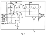
- FIGURE 1 is a schematic diagram of a differential multiplexer constructed in accordance with one embodiment of the present invention.
- Multiplexer 10 receives a first pair of complementary logic-level input signals IN1 and NIN1 and a second pair of complementary logic-level input signals IN2 and NIN2. Multiplexer 10 also receives complementary select signals SEL and NSEL to select either IN1 and NIN1 or IN2 and NIN2 as the signals to be driven to the output of multiplexer 10. While a two-input multiplexer is shown for ease of illustration, it will be understood that it could be a multiplexer with three or more inputs.
- Input signals IN1 and NIN1 are supplied to the gates of transistors 12 and 14, respectively.
- Transistors 12 and 14 have coupled sources.
- Select signal SEL is supplied to the gate of a transistor 16, which has a drain connected to the sources of transistors 12 and 14 and a source connected to a current source 18, which sources a current I 1 .
- select signal SEL causes transistor 16 to create either an open circuit or a closed circuit between transistors 12 and 14 and current source 18.
- input signals IN2 and NIN2 are supplied to the gates of transistors 20 and 22, respectively.
- Transistors 20 and 22 have coupled sources.
- Complementary select signal NSEL is supplied to the gate of a transistor 24, which has a drain connected to the sources of transistors 20 and 22 and a source connected to current source 18.
- complementary select signal NSEL causes transistor 24 to create either an open circuit or a closed circuit between transistors 20 and 22 and current source 18.
- Transistor 12 has a drain connected to a node 25.
- a resistor 26 having a resistance R is connected between node 25 and a voltage supply node 28, which carries a voltage V1.
- transistor 14 has a drain connected to a node 29.
- a resistor 30 having a resistance R is connected between node 29 and voltage supply node 28.
- transistor 20 has a drain connected to a node 31.
- a resistor 32 having a resistance R is connected between node 31 and a second voltage supply node 34, which carries a voltage V2.
- Transistor 22 has a drain connected to a node 35.
- a resistor 36 having a resistance R is connected between node 35 and voltage supply node 34.
- Supply voltages V1 and V2 are provided by a voltage supply 38, which receives select signals SEL and NSEL.
- Voltage supply 38 provides supply voltages V1 and V2 at different levels depending on the select inputs SEL and NSEL, as is described more fully below.
- Each output transistor 40, 42, 44 and 46 has a drain connected to a supply voltage VDD and a source connected to one of two current sources 48 and 50.
- Transistors 40 and 44 which receive their respective gate voltages from nodes 25 and 31, respectively, have sources connected to current source 48 via output node 52.
- Transistors 42 and 46 which receive their respective gate voltages from nodes 29 and 35, respectively, have sources connected to current source 50 via output node 54.
- An output signal OUT is generated by transistors 42 and 46 and current source 50 at output node 54.
- a complementary output signal NOUT is generated by transistors 40 and 44 and current source 48 at output node 52.
- multiplexer 10 is an integrated circuit created on a GaAs substrate.
- the transistor components of multiplexer 10 are GaAs n-channel MOSFETs with a channel length of 0.6 micrometres. Exemplary transistor widths and other circuit component values and voltages are listed in Table A according to reference numeral.
- Transistor Width (microns) Resistor Resistance (ohms) 12 15 26 3.2k 14 15 30 3.2k 16 15 32 3.2k 20 15 36 3.2k 22 15 24 15 Current Source Current 40 12 42 12 18 250 ⁇ A 44 12 48 220 ⁇ A 46 12 50 220 ⁇ A Voltage Supply Voltage Signal Levels V1 3.3 or 1.5 V INx/NINx 1.4/2.0 V V2 3.3 or 1.5 V SEL/NSEL 0.8/1.4 V VDD 3.3 V OUT/NOUT 2.4/3.0 V
- multiplexer 10 When select signal SEL is HIGH and NSEL is LOW, the current I 1 drawn by current source 18 is drawn entirely from the sources of transistors 12 and 14, while no current is conducted by transistors 20 and 22. In this state, input signals IN1 and NIN1 determine the values of output signals OUT and NOUT.
- one of the transistors 12 or 14 will conduct current I 1 , while the other transistor 12 or 14 will conduct no current.
- either node 25 or node 29 will carry the supply voltage V1
- the other node 25 or 29 will carry a voltage equal to V1 -I 1 * R. Because transistors 20 and 22 conduct no current, nodes 32 and 36 carry the supply voltage V2.
- voltage supply 38 When select signal SEL is HIGH, voltage supply 38 provides voltage V1 at a higher value, such as 3.3 volts, and voltage V2 at a lower value, such as 1.5 volts. With V1 at 3.3 volts, and an IR voltage drop of approximately 0.7 to 0.8 volts across either resistor 26 or resistor 30, one of the nodes 25 or 29 carries a voltage of approximately 2.5 volts, while the other node 25 or 29 carries a voltage of 3.3 volts.
- Current sources 48 and 50 ensure that transistors 40 and 42 act as source-followers, thereby producing one output signal OUT or NOUT at 3.0 volts, and the other output signal at 2.4 volts.
- the lower supply voltage (in this example V2) of 1.5 volts maintains the gates of (in this example) transistors 44 and 46 at 1.5 volts, thereby ensuring that these transistors are off and allowing transistors 40 and 42 to act as source-followers without interference or contention from transistors 44 and 46.
- select signal SEL When select signal SEL is LOW and NSEL is HIGH, it will be understood that the operation of multiplexer 10 is reversed, so that input signals IN2 and NIN2 determine the values of output signals OUT and NOUT. In this select state, either transistor 20 or 22 will conduct the current I 1 of current source 18. Voltage supply 38 generates supply voltage V1 at the lower value (e.g. 1.5 volts) and V2 at the higher value (e.g. 3.3 volts). Output transistors 44 and 46 will therefore act as source followers, while transistors 40 and 42 remain off.
- multiplexer 10 has significant advantages over an alternative multiplexer design in which resistors 26 and 32 are one and the same resistor, resistors 30 and 36 are one and the same resistor, nodes 25 and 31 are one and the same node, nodes 29 and 35 are one and the same node, output transistors 40 and 44 are one and the same transistor, and output transistors 42 and 46 are one and the same transistor.
- nodes 25 and 31 are effectively wire-ORed together, as are nodes 29 and 35.
- the joined node 25/31 has two transistors 12 and 20 connected to it, thereby doubling the Miller capacitance (gate-drain capacitance) on the node.
- Miller capacitance gate-drain capacitance
- This added capacitance slows the voltage swing at node 25/31, decreasing the maximum frequency or bandwidth attainable by the multiplexer.
- This bandwidth-limiting problem increases proportionally as the number of signals multiplexed by the multiplexer increases.
- input signals IN1, NIN1, IN2 and NIN2 may be live signals at all times regardless of the state of select signals SEL and NSEL, the Miller capacitance of transistors 12 and 20 creates capacitative coupling between the selected input signal and the non-selected input signal, thereby creating undesirable crosstalk.
- multiplexer 10 as shown in FIGURE 1 has, in essence, wire-ORed outputs and isolated inputs.
- the capacitance on each node 25, 29, 31 and 35 is decreased, thereby increasing the attainable frequency or bandwidth of multiplexer 10.
- transistors 40 and 44 are wire-ORed together at their sources. This doubles the amount of gate-source capacitance at output node 52.
- output transistors 40 and 44 are designed to drive a relatively large load capacitance, the effect of the additional gate-source capacitance on the output slew rate at output node 52 is negligible.
- the gate-source capacitance of the inactive output transistor 40 or 44 does not introduce any appreciable crosstalk into output signal NOUT.
- multiplexer 10 has a somewhat greater number of circuit components than the aforementioned alternative design, the design of multiplexer 10 is advantageous is those applications where maximum bandwidth and/or minimum crosstalk is desired.
- multiplexer 10 has been described herein as having GaAs MOSFETs as its transistor components, it will be understood that multiplexer 10 may be implemented on a silicon substrate and/or with bipolar transistors or other switching devices. If bipolar transistors are used, it will be appreciated that multiplexer 10 may advantageously be implemented in an emitter coupled logic (ECL) circuit.
- ECL emitter coupled logic
- signals, NIN1, NIN2 and OUT are eliminated, along with transistors 14, 22, 42 and 46, resistors 30 and 36 and current source 50.
- signals SEL and NSEL may both be used as previously described, or alternatively, signal NSEL may be eliminated and transistor 24 may be a p-channel transistor receiving select signal SEL at its gate. It will be appreciated that the advantageous aspects of multiplexer 10 are also exhibited by this alternative embodiment.
Landscapes
- Engineering & Computer Science (AREA)
- Microelectronics & Electronic Packaging (AREA)
- Computer Networks & Wireless Communication (AREA)
- Signal Processing (AREA)
- Electronic Switches (AREA)
Abstract
Description
| Transistor | Width (microns) | Resistor | Resistance (ohms) |
| 12 | 15 | 26 | 3.2 |
| 14 | 15 | 30 | 3.2 |
| 16 | 15 | 32 | 3.2 |
| 20 | 15 | 36 | 3.2 |
| 22 | 15 | ||
| 24 | 15 | Current Source | Current |
| 40 | 12 | ||
| 42 | 12 | 18 | |
| 44 | 12 | 48 | |
| 46 | 12 | 50 | 220µA |
| Voltage Supply | Voltage | Signal | Levels |
| V1 | 3.3 or 1.5 V | INx/NINx | 1.4/2.0 V |
| V2 | 3.3 or 1.5 V | SEL/NSEL | 0.8/1.4 V |
| VDD | 3.3 V | OUT/NOUT | 2.4/3.0 V |
Claims (10)
- A multiplexer comprising:a first input device operable to receive a first input signal and a first select signal, the first input device being further operable, when the first select signal has a first state, to generate a first voltage at a first node in response to the first input signal, the first input device being further operable, when the first select signal has a second state, to generate a first reference voltage at the first node,a second input device operable to receive a second input signal and a second select signal related to the first select signal, the second input device being further operable, when the second select signal has a first state, to generate a second voltage at a second node in response to the second input signal, the second input device being further operable, when the second select signal has a second state, to generate a second reference voltage at the second node,a first output buffer including an input terminal coupled to the first node, the first output buffer including an output terminal coupled to an output node, the first output buffer being operable to track at the output terminal the first voltage, the first output buffer being operable to present a high impedance at the output terminal when the first reference voltage is present at the first node; anda second output buffer including an input terminal coupled to the second node the second output buffer including an output terminal coupled to the output node, the second output buffer being operable to track at the output terminal the second voltage, the second output buffer being operable to present a high impedance at the output terminal when the second reference voltage is present at the second node.
- The multiplexer of claim 1, wherein the first input device comprises:a first input node operable to receive the first input signal;a first input transistor including a first terminal coupled to the first input node;a first voltage supply node carrying a first reference voltage;a first impedance connected between the first voltage supply node and a second terminal of the first input transistor; anda current source coupled to a third terminal of the first input transistor.
- The multiplexer of claim 2, wherein the second input device comprises:a second input node operable to receive the second input signal;a second input transistor including a first terminal coupled to the second input node, the second input transistor including a third terminal coupled to the current source;a second voltage supply node carrying a second reference voltage; anda second impedance connected between the second voltage supply node and a second terminal of the second input transistor.
- The multiplexer of claim 3, wherein the first input device comprises a first select transistor including a first terminal operable to receive the first select signal, the first select transistor including a second terminal connected to the third terminal of the first input transistor, the first select transistor including a third terminal connected to the current source.
- The multiplexer of claim 4, wherein the second input device comprises a second select transistor including a first terminal operable to receive the second select signal, the second select transistor including a second terminal connected to the third terminal of the second input transistor, the second select transistor including a third terminal connected to the current source.
- The multiplexer of claim 1, wherein the first output buffer comprises a first output transistor including a first terminal coupled to the first node, a second terminal coupled to a reference voltage source, and a third terminal coupled to the output node.
- The multiplexer of claim 6, wherein the second output buffer comprises a second output transistor including a first terminal coupled to the second node, a second terminal coupled to the reference voltage source, and a third terminal coupled to the output node.
- The multiplexer of claim 3, comprising a voltage supply operable to receive the first and second select signals, the voltage supply being operable to generate the first reference voltage at a first level and the second reference voltage at a second level in response to the first state'of the first select signal and the second state of the second select signal, the voltage supply being operable to generate the first reference voltage at the second level and the second reference voltage at the first level in response to the second state of the first select signal and the first state of the second select signal.
- A multiplexer comprising:a first input node operable to receive a first input signal;a second input node operable to receive a second input signal;a first input transistor including a first terminal coupled to the first input node;a second input transistor including a first terminal coupled to the second input node;a first voltage supply node carrying a first reference voltage;a second voltage supply node carrying a second reference voltage;a first resistor connected between the first voltage supply node and a second terminal of the first input transistor;a second resistor connected between the second voltage supply node and a second terminal of the second input transistor;a current source;a first select transistor including a first terminal operable to receive a first select signal, the first select transistor including a second terminal coupled to a third terminal of the first input transistor, the first select transistor including a third terminal coupled to the current source;a second select transistor including a first terminal operable to receive a second select signal related to the first select signal, the second select transistor including a second terminal coupled to a third terminal of the second input transistor, the second select transistor including a third terminal coupled to the current source;an output node;a first output transistor including a first terminal coupled to the second terminal of the first input transistor, the first output transistor including a third terminal coupled to the output node, the first output transistor being operable to generate a voltage at the third terminal of the first output transistor in response to a voltage received at the first terminal of the first output transistor when the voltage received at the first terminal of the first output transistor is within a first range, the first output transistor being operable to present a high impedance at the third terminal of the first output transistor when the voltage received at the first terminal of the first output transistor is within a second range; anda second output transistor including a first terminal coupled to the second terminal of the second input transistor, the second output transistor including a third terminal coupled to the third terminal of the first output transistor, the second output transistor being operable to generate a voltage at the third terminal of the second output transistor in response to a voltage received at the first terminal of the second output transistor when the voltage received at the first terminal of the second output transistor is within a third range, the second output transistor being operable to present a high impedance at the third terminal of the second output transistor when the voltage received at the first terminal of the second output transistor is within a fourth range.
- The multiplexer of claim 9, comprising a voltage supply operable to receive the first and second select signals, the voltage supply being operable to generate the first reference voltage at a first level and the second reference voltage at a second level lower than the first level in response to the first state of the first select signal and the second state of the second select signal, the voltage supply being operable to generate the first reference voltage at the second level and the second reference voltage at the first level in response to the second state of the first select signal and the first state of the second select signal.
Applications Claiming Priority (2)
| Application Number | Priority Date | Filing Date | Title |
|---|---|---|---|
| US208625 | 1998-12-08 | ||
| US09/208,625 US6310509B1 (en) | 1998-12-08 | 1998-12-08 | Differential multiplexer with high bandwidth and reduced crosstalk |
Publications (2)
| Publication Number | Publication Date |
|---|---|
| EP1017193A2 true EP1017193A2 (en) | 2000-07-05 |
| EP1017193A3 EP1017193A3 (en) | 2002-07-17 |
Family
ID=22775335
Family Applications (1)
| Application Number | Title | Priority Date | Filing Date |
|---|---|---|---|
| EP99309733A Withdrawn EP1017193A3 (en) | 1998-12-08 | 1999-12-03 | Multiplexer |
Country Status (3)
| Country | Link |
|---|---|
| US (1) | US6310509B1 (en) |
| EP (1) | EP1017193A3 (en) |
| JP (1) | JP2000236244A (en) |
Cited By (2)
| Publication number | Priority date | Publication date | Assignee | Title |
|---|---|---|---|---|
| EP1187382A3 (en) * | 2000-09-05 | 2005-07-20 | Agilent Technologies, Inc. (a Delaware corporation) | Multiplexer with channel sectioning, selectively actuated current sources, and common-base amplifiers |
| US7609799B2 (en) | 2005-09-02 | 2009-10-27 | Cypress Semiconductor Corporation | Circuit, system, and method for multiplexing signals with reduced jitter |
Families Citing this family (12)
| Publication number | Priority date | Publication date | Assignee | Title |
|---|---|---|---|---|
| JPH11205268A (en) * | 1998-01-16 | 1999-07-30 | Sony Corp | Signal multiplexing circuit |
| US6549037B1 (en) * | 2000-06-26 | 2003-04-15 | Intel Corporation | Apparatus and circuit having reduced leakage current and method therefor |
| US6353338B1 (en) * | 2000-09-28 | 2002-03-05 | Lsi Logic Corporation | Reduced-swing differential output buffer with idle function |
| US6614291B1 (en) * | 2001-06-15 | 2003-09-02 | Lattice Semiconductor Corp. | Low voltage, high speed CMOS CML latch and MUX devices |
| JP3810298B2 (en) * | 2001-10-19 | 2006-08-16 | 富士通株式会社 | Multiplexer circuit |
| US7123074B2 (en) * | 2004-02-24 | 2006-10-17 | Micrel, Inc. | Method and system for multichannel-isolation-technique multiplexer |
| US7378835B2 (en) * | 2006-06-07 | 2008-05-27 | National Instruments Corporation | Interleaved differential multiplexer |
| KR100911159B1 (en) * | 2007-08-30 | 2009-08-06 | 한국과학기술원 | Multiplexer circuit |
| CN106549656A (en) | 2016-11-22 | 2017-03-29 | 章策珉 | A kind of frequency expands device |
| CN106374919B (en) | 2016-11-22 | 2020-02-18 | 成都仕芯半导体有限公司 | Frequency expanding device based on multi-path selector |
| CN107453743A (en) * | 2017-05-04 | 2017-12-08 | 李海莲 | A kind of application method of wireless communication field multiplexer |
| US12074593B1 (en) * | 2021-10-31 | 2024-08-27 | Synopsys, Inc. | High-voltage tolerant multiplexer |
Family Cites Families (10)
| Publication number | Priority date | Publication date | Assignee | Title |
|---|---|---|---|---|
| US4963767A (en) * | 1988-08-25 | 1990-10-16 | National Semiconductor Corporation | Two-level ECL multiplexer without emitter dotting |
| JPH02134006A (en) * | 1988-11-14 | 1990-05-23 | Nec Corp | Amplifying circuit |
| CA2108883C (en) * | 1992-02-20 | 1999-05-04 | Petre Popescu | Differential emitter coupled logic circuit |
| US5298810A (en) * | 1992-09-11 | 1994-03-29 | Cypress Semiconductor Corporation | BiCMOS CMOS/ECL data multiplexer |
| US5485110A (en) * | 1994-02-01 | 1996-01-16 | Motorola Inc. | ECL differential multiplexing circuit |
| US5420529A (en) * | 1994-05-19 | 1995-05-30 | Northern Telecom Limited | Current steering switch and hybrid BiCMOS multiplexer with CMOS commutation signal and CML/ECL data signals |
| FR2724073A1 (en) * | 1994-08-31 | 1996-03-01 | Sgs Thomson Microelectronics | LOGIC CIRCUIT WITH DIFFERENTIAL STAGES |
| US6137340A (en) * | 1998-08-11 | 2000-10-24 | Fairchild Semiconductor Corp | Low voltage, high speed multiplexer |
| US6239646B1 (en) * | 1998-10-29 | 2001-05-29 | Cypress Semiconductor Corp. | High-speed, multiple-input multiplexer scheme |
| US6211722B1 (en) * | 1999-03-19 | 2001-04-03 | Lucent Technologies Inc. | Low voltage high speed multiplexer and latch |
-
1998
- 1998-12-08 US US09/208,625 patent/US6310509B1/en not_active Expired - Fee Related
-
1999
- 1999-11-19 JP JP11330476A patent/JP2000236244A/en active Pending
- 1999-12-03 EP EP99309733A patent/EP1017193A3/en not_active Withdrawn
Cited By (6)
| Publication number | Priority date | Publication date | Assignee | Title |
|---|---|---|---|---|
| EP1187382A3 (en) * | 2000-09-05 | 2005-07-20 | Agilent Technologies, Inc. (a Delaware corporation) | Multiplexer with channel sectioning, selectively actuated current sources, and common-base amplifiers |
| KR100722110B1 (en) * | 2000-09-05 | 2007-05-25 | 아바고 테크놀로지스 제너럴 아이피 (싱가포르) 피티이 리미티드 | Multiplexer with channel sectioning, selectively actuated current sources, and common-base amplifiers |
| US7609799B2 (en) | 2005-09-02 | 2009-10-27 | Cypress Semiconductor Corporation | Circuit, system, and method for multiplexing signals with reduced jitter |
| WO2007027833A3 (en) * | 2005-09-02 | 2010-09-02 | Cypress Semiconductor Corp. | Circuit, system and multiplexing signals with reduced jitter |
| US7899145B2 (en) | 2005-09-02 | 2011-03-01 | Cypress Semiconductor Corporation | Circuit, system, and method for multiplexing signals with reduced jitter |
| US8290109B2 (en) | 2005-09-02 | 2012-10-16 | Cypress Semiconductor Corporation | Circuit, system and method for multiplexing signals with reduced jitter |
Also Published As
| Publication number | Publication date |
|---|---|
| JP2000236244A (en) | 2000-08-29 |
| US6310509B1 (en) | 2001-10-30 |
| EP1017193A3 (en) | 2002-07-17 |
Similar Documents
| Publication | Publication Date | Title |
|---|---|---|
| US5206544A (en) | CMOS off-chip driver with reduced signal swing and reduced power supply disturbance | |
| US7088166B1 (en) | LVDS input circuit with extended common mode range | |
| US5165046A (en) | High speed CMOS driver circuit | |
| US7710149B1 (en) | Input buffer for multiple differential I/O standards | |
| EP0449251B1 (en) | Output circuit | |
| US6982583B2 (en) | Current-controlled CMOS circuit using higher voltage supply in low voltage CMOS process | |
| US6031394A (en) | Low voltage CMOS circuit for on/off chip drive at high voltage | |
| US20080246511A1 (en) | Differential Drive Circuit and Electronic Apparatus Incorporating the Same | |
| EP1017193A2 (en) | Multiplexer | |
| US6911855B2 (en) | Current-controlled CMOS circuit using higher voltage supply in low voltage CMOS process | |
| US6617892B2 (en) | Single ended interconnect systems | |
| US6320422B1 (en) | Complementary source coupled logic | |
| JP3240042B2 (en) | Semiconductor output circuit | |
| EP0196113B1 (en) | Tri-state buffer circuit | |
| EP0569127A2 (en) | CMOS ECL translator with incorporated latch | |
| US4943740A (en) | Ultra fast logic | |
| US6788103B1 (en) | Activ shunt-peaked logic gates | |
| EP0347083B1 (en) | TTL output driver gate configuration | |
| JPS5842320A (en) | integrated circuit power supply | |
| US6580323B2 (en) | Interface circuit for a differential signal | |
| US4958132A (en) | Complementary metal-oxide-semiconductor translator | |
| US4977338A (en) | High speed bipolar-MOS logic circuit including a series coupled arrangement of a bipolar transistor and a logic block having a MOSFET | |
| US6329834B1 (en) | Reduction of switching noise in integrated circuits | |
| EP0435389B1 (en) | Differential input, differential output BICMOS multiplexers and logic gates and an adder utilizing the same | |
| JP3320757B2 (en) | Apparatus and method for converting voltage |
Legal Events
| Date | Code | Title | Description |
|---|---|---|---|
| PUAI | Public reference made under article 153(3) epc to a published international application that has entered the european phase |
Free format text: ORIGINAL CODE: 0009012 |
|
| AK | Designated contracting states |
Kind code of ref document: A2 Designated state(s): AT BE CH CY DE DK ES FI FR GB GR IE IT LI LU MC NL PT SE |
|
| AX | Request for extension of the european patent |
Free format text: AL;LT;LV;MK;RO;SI |
|
| PUAL | Search report despatched |
Free format text: ORIGINAL CODE: 0009013 |
|
| AK | Designated contracting states |
Kind code of ref document: A3 Designated state(s): AT BE CH CY DE DK ES FI FR GB GR IE IT LI LU MC NL PT SE |
|
| AX | Request for extension of the european patent |
Free format text: AL;LT;LV;MK;RO;SI |
|
| RIC1 | Information provided on ipc code assigned before grant |
Free format text: 7H 04J 3/04 A, 7H 03K 17/62 B |
|
| AKX | Designation fees paid | ||
| REG | Reference to a national code |
Ref country code: DE Ref legal event code: 8566 |
|
| STAA | Information on the status of an ep patent application or granted ep patent |
Free format text: STATUS: THE APPLICATION IS DEEMED TO BE WITHDRAWN |
|
| 18D | Application deemed to be withdrawn |
Effective date: 20030118 |