EP1018201B1 - Halbleiterhochspannungskurzschlussschaltung - Google Patents
Halbleiterhochspannungskurzschlussschaltung Download PDFInfo
- Publication number
- EP1018201B1 EP1018201B1 EP96932313A EP96932313A EP1018201B1 EP 1018201 B1 EP1018201 B1 EP 1018201B1 EP 96932313 A EP96932313 A EP 96932313A EP 96932313 A EP96932313 A EP 96932313A EP 1018201 B1 EP1018201 B1 EP 1018201B1
- Authority
- EP
- European Patent Office
- Prior art keywords
- stage
- high voltage
- component
- state
- shunting
- Prior art date
- Legal status (The legal status is an assumption and is not a legal conclusion. Google has not performed a legal analysis and makes no representation as to the accuracy of the status listed.)
- Expired - Lifetime
Links
- 230000001105 regulatory effect Effects 0.000 claims 12
- 230000007423 decrease Effects 0.000 claims 3
- 230000008878 coupling Effects 0.000 claims 2
- 238000010168 coupling process Methods 0.000 claims 2
- 238000005859 coupling reaction Methods 0.000 claims 2
- 230000005669 field effect Effects 0.000 claims 2
- 239000003990 capacitor Substances 0.000 description 9
- 230000008901 benefit Effects 0.000 description 6
- 238000007599 discharging Methods 0.000 description 5
- 238000000034 method Methods 0.000 description 4
- 230000008569 process Effects 0.000 description 3
- 238000010276 construction Methods 0.000 description 2
- 230000000694 effects Effects 0.000 description 2
- 230000002285 radioactive effect Effects 0.000 description 2
- YZCKVEUIGOORGS-NJFSPNSNSA-N Tritium Chemical compound [3H] YZCKVEUIGOORGS-NJFSPNSNSA-N 0.000 description 1
- 230000009471 action Effects 0.000 description 1
- 230000003466 anti-cipated effect Effects 0.000 description 1
- 238000013459 approach Methods 0.000 description 1
- 238000005513 bias potential Methods 0.000 description 1
- 230000000903 blocking effect Effects 0.000 description 1
- 230000015556 catabolic process Effects 0.000 description 1
- 239000002360 explosive Substances 0.000 description 1
- 230000006698 induction Effects 0.000 description 1
- 230000001939 inductive effect Effects 0.000 description 1
- 238000012986 modification Methods 0.000 description 1
- 230000004048 modification Effects 0.000 description 1
- 230000001960 triggered effect Effects 0.000 description 1
- 229910052722 tritium Inorganic materials 0.000 description 1
Images

Classifications
-
- H—ELECTRICITY
- H02—GENERATION; CONVERSION OR DISTRIBUTION OF ELECTRIC POWER
- H02H—EMERGENCY PROTECTIVE CIRCUIT ARRANGEMENTS
- H02H9/00—Emergency protective circuit arrangements for limiting excess current or voltage without disconnection
- H02H9/04—Emergency protective circuit arrangements for limiting excess current or voltage without disconnection responsive to excess voltage
- H02H9/041—Emergency protective circuit arrangements for limiting excess current or voltage without disconnection responsive to excess voltage using a short-circuiting device
Definitions
- the invention relates generally to crowbar circuits, and more particularly to a solid-state crowbar circuit for shunting a large current at high voltage to a safe potential.
- Circuits designed to accomplish this are known as crowbar circuits or energy diverters. They are designed to quickly reduce a high potential to a low potential in order to prevent damage to equipment connected to the power supply, and also for the safety of those who may come in contact with exposed high voltage components.
- Helmet-mounted avionics display for military pilots.
- Helmet-mounted displays can require up to 20,000 volts to drive a cathode ray tube (CRT) in the display.
- CRT cathode ray tube
- FIGURE 1 one prior art type of crowbar circuit uses a spark gap 28 to quickly discharge a high voltage source potential.
- a high voltage source 20 is connected to a cathode ray tube (CRT) display 26 via electrical connectors 22 and 24.
- Connectors 22 and 24 allow the display to be disconnected from the power supply.
- a trigger circuit 30 is used to apply a trigger pulse to the spark gap which can be a small canister filled with a normally nonconducting radioactive gas.
- the trigger pulse produces a small arc within the spark gap, which begins to ionize the gas within the device.
- the spark gap 28 becomes conductive, and current begins to flow from the high voltage source through the spark gap to ground.
- An avalanche effect is started, and the ionization increases with the increased current flow. This causes the high voltage potential to decay rapidly, as the initial charge is quickly channeled to ground. Once the current falls to a value insufficient to maintain arc conditions, current flow ceases and the gap returns to the nonconductive state.
- spark gap 28 is a fairly complex component containing a trace amount of radioactive tritium gas, for example. Because the rapid ionization of the gas quickly wears out the device, the spark gap must be periodically replaced at substantial cost. The spark gap also must be correctly sized for each application. Since a spark gap only operates within a narrow range of voltages, different spark gaps must be used in different environments. The operation of a spark gap is further limited in that a spark gap will not discharge a voltage that is less than 40% of its rating. As a result, designing with spark gaps is not an easy process.
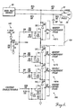
- FIGURE 3 is a graph depicting a typical spark gap's voltage ringing.
- the left vertical axis represents the voltage, and the lower horizontal axis represents time.
- a plot of the output potential across the spark gap is represented by a line 60.
- the spark gap is triggered to discharge the high potential voltage.
- the near vertical slope of line 60 between times T 1 and T 2 the voltage quickly drops to near a ground potential.
- a typical spark gap crowbar circuit will be able to discharge a 13,000 volt potential in less than 15 nanoseconds.
- a result of this rapid discharge is a voltage ringing induced between times T 2 and T 3 . That is, the voltage across the spark gap partially rebounds before decaying down to a steady ground potential. In a typical spark gap device, the voltage rebound can be significant.
- the initial value of the ringing voltage may reach a level of 400 volts, a value that can cause component damage due to electrostatic discharge.
- the existence of a potential of even a few hundred volts can potentially harm a user if sparks or other arcs are created by the crowbar circuit.
- FIG. 2 Another crowbar circuit design is a transformer-driven transistor array of the type shown diagrammatically in FIGURE 2, which operates in the same environment as the circuits of FIGURE 1. That is, high voltage source 20 is connected to display 26 via connectors 22 and 24. Instead of using a spark gap device, however, the crowbar circuit of FIGURE 2 relies upon a number of transistor stages 40. A high voltage is applied across a number of these transistor stages, which are connected in a cascade configuration. In normal operation, the transistors are biased off so that no current will flow through the transistor stages 40. Each transistor stage 40 is coupled via a shared transformer 42 to a drive circuit 44. When a high voltage is to be discharged, the drive chcuit is turned on, biasing each of the transistor stages 40 into saturation.
- each transistor stage 40 When in saturation, each transistor stage 40 conducts current between the high voltage source and ground. Because all transistor stages are turned on simultaneously, the result is a rapid decay of a high voltage potential down to a ground potential.
- Typical transformer-driven transistor array circuits can discharge a 13,000 volt potential in under five microseconds. Once the drive circuit is turned off, the transistor bias potential is allowed to leak away, returning the transistors to nonconductive operation.
- a disadvantage of a crowbar circuit constructed with a transformer-driven transistor array is that the transformer needed to simultaneously turn on all of the transistor stages 40 is a large and expensive device (the transformer must withstand the total output voltage). Additionally, because the circuit can discharge a high potential within less than five microseconds, the circuit also exhibits a voltage ringing as shown in FIGURE 3. That is, much like a spark gap crowbar circuit, the rapid discharge of the high voltage source results in a voltage rebound of several hundred volts which could potentially impose a danger both to the circuit and to people nearby.
- the present invention provides a solid-state crowbar circuit for shunting a large current at high voltage to a safe potential.
- the circuit consists of multiple transistor stages connected in cascade, one end of the circuit being connected to a high voltage source, and the other end of the circuit being coupled to ground through a discharge resistance.
- a diode is connected in parallel with the transistor of each stage.
- each stage has a resistor connected between the gate and source of its transistor. The gate-to-source voltage, i.e., current through the resistor, determines whether or not the transistor of that stage is "on" or "off.”
- the transistor stage immediately connected to the discharge resistance is referred to herein as the driver stage.
- the driver stage has an enable input allowing the driver transistor to be biased on. Normally, however, the driver stage is biased off so that the stage is nonconducting.
- the transistor stages connected between the high voltage source and the driver stage are referred to herein as the component stages. Each of these stages is similarly normally biased in an off state so that the stage is nonconducting.
- the impedance seen by the high voltage supply is equal to the sum of the transistor off resistances. In practice, the off impedance of each transistor stage exceeds one gigaohm. Therefore no current typically flows through the crowbar circuit when it is disabled.
- an enable signal is generated to bias the driver stage of the crowbar circuit on.
- the driver stage provides a current path through the gate-to-source resistor of the component stage adjacent to the driver stage, which then also begins to conduct to provide a current path through the gate-to-source resistor of the next component stage.
- This process continues with each component stage turning on after the stage below it turns on. Eventually, all component stages are turned on, creating a current path through the transistors of all stages from the high voltage source through the discharge resistance to ground.
- the impedance across it changes from an essentially open circuit to an essentially closed circuit.
- the closed circuit on state there is negligible voltage drop across it, such that the voltage of the source is applied across fewer and fewer of the series connected diodes.
- the ratings of the diodes remote from the driver stage are exceeded and they operate in avalanche mode, providing a separate current path around the transistors of the upper component stages. Current therefore flows from the high voltage source, through the avalanching diodes, then through the conducting transistors and the discharge resistance to ground, as the upper component stages continue to turn on one-by-one.
- the discharge resistance has the effect of maintaining an almost constant current from source to ground so that the source voltage is discharged essentially linearly, over a selected period long enough to prevent potentially harmful flyback or ringing.
- the series connected diodes also act as a voltage clamp to limit the voltage that may be applied by the high voltage source to the load CRT. If a voltage is generated that exceeds the sum of all the avalanche voltages of the diodes, the diodes will enter avalanche conduction and discharge the excess potential. This over-voltage clamp protection ensures that voltages above a specified value will not be accidentally supplied to the load.
- An advantage of the disclosed invention is that it provides a rapid linear discharge of high voltage without inducing flyback or ringing. Ringing is minimized by discharging the electrical current at a controlled rate.
- the controlled discharge rate not only reduces voltage ringing, it also places less stress upon the components in the crowbar circuit.
- a further advantage of this circuit is that it uses solid-state components which are readily available and relatively inexpensive. Because solid-state components are used, the entire crowbar circuit can be constructed to displace a very small volume and be of minimal weight. It is also easier to tailor the crowbar circuit to the precise high voltage that is to be discharged by varying the number of component stages in the circuit. That is, the number of component stages may be varied depending upon the anticipated maximum voltage that must be shunted. This allows the crowbar circuit to be simply and easily adjusted to operate in different environment.
- a still further advantage of this invention is that it provides over-voltage clamp protection for the high voltage power supply and associated external load, That is, if the voltage exceeds the sum of the avalanche values for each of the diodes, the diodes will enter a conductive state to discharge the excess voltage. This ensures that voltage over a set level will not be applied to the load.
- this circuit it is also an advantage of this circuit that the enable signal used to drive the circuit is directly coupled to the driver stage. Unlike spark gap or transformer-driven transistor array crowbar circuits, there is no magnetic induction required to trigger the operation of this circuit. This reduces the possibility that stray electric or magnetic fields will unintentionally trigger the discharge of the high voltage source.
- the disclosed circuit is also constructed to allow multiple high voltage levels to be simultaneously discharged, such as both the anode and focus voltages of a CRT which may differ by several thousand volts. This eliminates the use of more than one crowbar circuit in a given environment.
- FIGURE 4 shows a preferred embodiment of a solid-state crowbar circuit 100 in accordance with the present invention.
- the crowbar circuit 100 is shown operating in the same environment discussed above. That is, a high voltage source 20 is connected to a CRT display 26 via two connectors 22 and 24. The CRT display 26 may be separated from the high voltage source 20 by disconnecting the connectors. While the preferred embodiment of crowbar circuit 100 is shown operating in this environment, those skilled in the art will recognize that the crowbar circuit disclosed herein can be used in any application where it is desired to reduce a high voltage potential to near ground potential, or any other specified potential, in a short period of time.
- Crowbar circuit 100 consists of a number of component stages 102a, 102b, ... 102n connected in cascade with a driver stage 104 that includes discharge resistor RS.
- the discharge resistor RS is connected to ground.
- the component stages 102a, 102b, ... 102n and driver stage 104 are initially biased “off" such that no current flows from the high voltage source 20 through the component and driver stages to ground.
- an enable signal is applied to the driver stage 104.
- the driver stage 104 becomes biased on and begins to provide a current path for the adjacent component stage 102a which then turns on and provides a current path for the adjacent stage 102b, which then turns on, and so on.
- the component stages 102a, 102b, ... 102n are biased on sequentially, beginning with the component stage closest to the driver stage, and ending with the component stage that is connected to the high voltage source.
- a diode DD is connected in parallel with each stage and, as the stages turn on sequentially such that there is little voltage drop across those stages, eventually the diodes more remote from the driver operate in avalanche to provide a current path from the source to ground.
- the sequential biasing of the component stages in conjunction with the discharge resistor RS results in a controlled linear drop of the high voltage potential to close to a ground potential within a short period of time. Because the potential drop is tightly controlled in comparison to the prior art crowbar circuits, there is reduced stress placed on the components of the circuit and no potentially harmful voltage ringing following the voltage drop.
- each component stage 102a, 102b, ... 102n is constructed with the same circuit elements.
- a generic component stage 102n will therefore be discussed as representative of all the component stages.
- Component stage 102n is constructed around a transistor TR, which in the preferred embodiment of the circuit is a MOSFET.
- Diode DD is connected across the drain and source of the transistor in parallel with a capacitor CD.
- a resistor RG is connected across the gate and source of the transistor in parallel with a zener diode ZG.
- Resistor RG and zener diode ZG are selected to prevent transistor conduction due to leakage current during biased-off operation, to generally protect the transistor from gate-to-source stress during biased-on operation, and to provide the desired gate-to-source voltage to turn the associated transistor on when a current path to ground is provided.
- circuit elements for each component stage are as follows: Component Part Number or Rating Diode DD BYJ96D, BYD37M Capacitor CD 22 pF 1808N100J202N, VJ1808A220JXGA Zener Diode ZG 15V rating Resistor RG 47 K ohms MOSFET TR IRFBG20, IRFR420, IRFRC20
- Bias circuit 140 consists of a diode DRB connected on one end to a positive voltage source (+ BIAS) and on the other end to a resistor RR and a capacitor CR. Diode DRB is selected to ensure that reverse current will not flow into the positive voltage source (+ BIAS). In a preferred embodiment of the crowbar circuit, the positive voltage source must provide a voltage greater than 30 volts VDC.
- the shared bias circuit is coupled to each component stage by a diode DB in series with a resistor RB. Diodes DB are selected to ensure that reverse current will not flow from the high voltage source 20 to the bias circuit 140.
- Resistors RB are sized to limit the current flow from the bias circuit 140 to the component stages 102a, 102b, ... 102n.
- the circuit elements of bias circuit 140 and associated component stages are as follows: Component Part Number or Rating Diode DRB 1N5617 Resistor RR 1 M ohm Capacitor CR 0.033 uF Diode DB M160FG, ESJA92-12 Resistor RB 10 K ohm
- Driver stage 104 is similar to component stages 102a, 102b, ... 102n in that it is constructed around a transistor TR, preferably a MOSFET.
- Discharge impedance preferably a resistor RS, is connected between the source of transistor TR and ground.
- the discharge resistor is selected to have a peak power capability sufficient to handle the energy shunted from high voltage source 20.
- Diode DD and capacitor CD serve the same functions as they do in the component stages, that is, they are selected to provide over-voltage protection for the circuit.
- Zener diode ZG connected between the gate of the transistor and ground, is sized to limit the voltage applied to the MOSFET gate.
- Resistor RG connected across the transistor gate and source is selected to provide sufficient gate-to-source voltage to turn the driver transistor on when an enable signal is received.
- a resistor RIN and capacitor CG network is connected between an enable input and the gate of the driver transistor. The network is designed to hold constant and filter out noise disturbance from the gate-to-source connection of the driver transistor.
- the driver circuit components are as follows: Component Part Number or Rating Transistor TR IRFBG20, IRFR420, IRFRC20 Diode DD BYJ96D, BYD37M Capacitor CD 22 pF 1808N100J202N, VJ1808A220JXGA Capacitor CG 0.01 uF Zener diode ZG 15V Resistor RG 47 K ohm Resistor RIN 1 K ohm
- the crowbar circuit 100 in one mode of operation, operates as a high voltage clamp to limit the voltage that may be applied by high voltage source 20 to a load.
- diodes DD operate in avalanche when a voltage exceeding a maximum desired voltage is generated by high voltage source 20. Diodes rated at 1,000 volts will typically avalanche at 1,100 to 1,200 volts. If, for example, the crowbar circuit consisted of twelve component stages plus one driver stage, the series connection of diodes DD would avalanche when the applied voltage exceeds between 13,000 and 15,600 volts (13 stages * 1,000 to 1,200 volts/stage).
- the voltage across the crowbar circuit 100 is limited to the sum total of the individual diode avalanches. This protects CRT display 26 or other load from breakdowns in the high voltage source or application of an external potential.
- the transistor avalanche rating is selected to be higher than that of the diodes. For example, the transistors may be selected to have an operating limit of between 1,200 and 1,500 volts. The diodes will therefore always enter avalanche before the transistors.
- crowbar circuit 100 is used to rapidly and substantially linearly reduce a high voltage potential to close to ground.
- the number of component stages used in the crowbar circuit directly determines the voltage level that may be shunted. Each component stage contributes to discharging a voltage potential equal to the maximum avalanche voltage of that stage.
- diodes DD are selected to avalanche before transistors TR. Therefore, the diode rating of each component stage 102a, 102b, ... 102n is used to determine the number of component stages necessary to discharge a particular voltage.
- the operating voltage of the high voltage source were 13,000 volts and if diodes rated at 1,000 volts are used in the crowbar circuit, a total of twelve component stages would be required in the crowbar circuit.
- the total operating voltage of the twelve diodes in the component stages and the single diode in the driver stage would add to a number approximating the required operating voltage of 13,000 volts.
- the use of thirteen transistor stages with 1,000 volt diodes in the crowbar circuit will hereinafter be referred to as a representative embodiment of the circuit.
- component stages 102a, 102b, ... 102n are biased-off so that the transistors are nonconducting. This allows component stages 102a, 102b,... 102n to "float.”
- the bias circuit 140 provides sufficient potential to the gates of component stage transistors TR so that they will become biased on when the gate-to-source turn-on voltage is exceeded by current flow through the associated resistor RG.
- driver stage 104 is biased off, ensuring that no current flows through discharge resistor RS.
- the impedance of crowbar circuit 100 as measured from high voltage source 20 to ground is very high. With the off impedance of each stage exceeding one gigaohm, the crowbar circuit acts essentially as an open circuit. In the biased off operation, the high-voltage source therefore directly supplies power to CRT display 26.
- an enable signal is applied to driver stage 104.
- a 15 V signal is applied to resistor RIN of the driver stage.
- the positive voltage signal is applied across resistors RIN, RG and RS, and the voltage developed across resistor RG is in excess of the driver transistor's gate-to-source threshold potential. The driver transistor is therefore biased on.
- component stage 102a After the driver transistor is biased on, a current path is provided from the component stage bias circuit 140, through diode DB, resistor RB and resistor RG of the adjacent component stage 102a, and through the driver transistor and discharge resistance to ground.
- component stage 102a When the voltage across RG rises sufficiently above the gate-to-source potential threshold of component transistor TR, component stage 102a is biased on. This process repeats for each component stage.
- the transistor TR of each component stage remains biased off, and nonconducting, while the component stages located nearest the driver stage sequentially enter conduction. That is, component stage 102a enters conduction, followed by component stage 102b, and proceeding until component stage 102n is conducting.
- the high voltage initially applied across all of the component and driver stages is essentially applied across fewer and fewer component stages whose transistors are still biased off.
- the per stage voltage is sufficiently great to force the diodes of the off-biased stages into avalanche, allowing current to flow from the high voltage potential through the avalanching diodes to the first component stage 102a, 102b, ... 102n that is conducting.
- the current then flows through the remaining biased-on transistors of each component stage, driver transistor TR, discharge resistor RS, and finally to ground.
- the component stages continue to turn on sequentially. The result is that over a very short period, but nevertheless not instantaneously, current flows from the high voltage potential through the discharge resistor to ground.
- the rate of current discharge is controlled by the discharge resistor RS acting in conjunction with the driver stage.
- transistors 120a, 120b, ... 120n of all the component sections have been turned on and the potential is discharged down to a very low value.
- a 13,000 volt DC output potential was discharged to 30 volts DC in around 100 microseconds. This was achieved with a 400 milliamp discharge current that was maintained relatively constant throughout the discharge period. Since the voltage discharge is performed in a controlled (and almost linear) manner, there is minimal output voltage ringing.
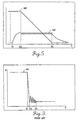
- FIGURE 5 is a representative graph of the voltage and current levels in an actual embodiment of the crowbar circuit 100.
- Line 180 represents the voltage measured across the crowbar circuit, from the high voltage source to ground.
- Line 182 represents the current flow through the driver stage 104.
- the graph provides an approximation of the operating characteristics of the circuit.
- an enable signal is generated to bias the driver stage 104 on.
- the current in the driver stage begins to rise.
- T 2 a sufficient number of the component stages have been turned on that the diodes DD of the other stages avalanche. As each subsequent component stage enters conduction, the voltage across the crowbar circuit linearly drops as indicated by the downward slope of line 180.
- the current through the driver stage 104 remains approximately constant, as evidenced by the zero slope of line 182.
- the high voltage has been discharged to a suitably low potential (close to ground).
- the current through the driver stage 104 decays to zero. It will be appreciated by those skilled in the art that the overall discharge time, rate, and current limit may be adjusted by appropriate selection of circuit components.
- a feedback diode DF is included to connect the focus of CRT display 26 with crowbar circuit 100 at a point distinct from the point connected to high voltage source 20.
- a focus of a CRT display typically operates at a voltage level several thousand volts below that of an anode of a CRT display.
- the focus of display 26 is maintained at 3,000 VDC. Discharging this voltage only requires two component stages to be connected to the driver stage. As shown in FIGURE 4, it is therefore possible to directly couple the reduced focus voltage to a point immediately following component stage 102b.
- Diode DF is a high voltage diode provided to isolate the anode potential from the focus potential.
- an X100FG diode is used.
- the crowbar circuit also limits the maximum voltage that can be applied at the focus terminal by the clamping action of the diode DD between the focus terminal and ground.
- an advantage of the crowbar circuit 100 is that a voltage discharge is handled in a controlled manner to prevent ringing in the voltage output. This eliminates the safety concerns associated with voltages that would rebound to several hundred volts. It will also be recognized that, unlike prior art crowbar circuits, the crowbar circuit of the present invention relies upon all solid-state devices in its construction. The present circuit eliminates the use of magnetically-coupled devices, such as transformers, for triggering the discharge operation. Constructing the crowbar circuit from solid-state devices saves weight, circuit board space, and improves reliability of operation.
- the disclosed crowbar circuit is highly flexible in that it may be used to discharge any range of voltages by appropriate selection of components and inclusion of the appropriate number of component stages in the circuit. Multiple voltage levels may also be simultaneously discharged by connecting the voltage level following the appropriate component stage.
- the disclosed circuit is therefore easily adapted to many different environments.
- the voltage clamp operation is preferably handled by diodes DD.
- the disclosed crowbar circuit 100 can also provide over-voltage protection without the diodes by selection of durable transistors with ratings that allow the transistors to operate in avalanche and provide a conductive path between the high voltage source and the driver stage. This method of operation is not preferred, however,. because operating the transistors in avalanche places unwanted stress on the components. Similarly, when discharging an undesirably high voltage to ground the circuit could also operate without diodes DD.
- the transistors would operate in avalanche to allow the current to reach those stages that have entered conduction. As mentioned above, however, this mode of operation places unnecessary stress on the components. Therefore, diodes will typically be employed in the preferred embodiment of crowbar circuit 100. It is an object of the appended claims to cover all modifications and variations as come within the scope of the invention.
Landscapes
- Generation Of Surge Voltage And Current (AREA)
Claims (25)
- Festkörper-Überspannungsschutzschaltung zum Parallelschalten einer an einem Hochspannungsanschluß anstehenden Hochspannung zu einem für ein vorbestimmtes Potential vorgesehenen Anschluß, dessen vorbestimmtes Potential viel geringer ist als die Hochspannung, umfassend:(a) eine erste Komponentenstufe, die an den Hochspannungsanschluß gekoppelt und betreibbar ist zum Leiten eines Stromflusses in einem Leitungspfad von dem Hochspannungsanschluß, wenn die erste Komponentenstufe in einen Ein-Zustand vorgespannt ist, wobei die erste Komponentenstufe normalerweise in einen Aus-Zustand vorgespannt ist, so daß die erste Komponentenstufe keinen Strom leitet;(b) eine Treiberstufe, die an die erste Komponentenstufe gekoppelt ist und betrieben wird, um einen Strom entlang dem Leitungspfad bei Vorspannung in den Ein-Zustand zu regulieren, wobei die Treiberstufe eine Entladungsimpedanz besitzt, die an den Anschluß für vorbestimmtes Potential gekoppelt ist, wobei die Treiberstufe normalerweise In einen Aus-Zustand vorgespannt ist, so daß sie den Strom nicht reguliert;(c) eine an die Treiberstufe gekoppelte Freigabequelle zum Erzeugen eines Freigabesignals, welches die Treiberstufe in den Ein-Zustand vorspannt und einen regulierten Strom durch die Entladungsimpedanz hin zu dem Anschluß für vorbestimmtes Potential erzeugt, wobei der regulierte Strom weiterhin die erste Komponentenstufe in einen Ein-Zustand vorspannt und dadurch die Hochspannung zu dem vorbestimmten Potential parallelschaltet durch Entladung entlang dem Leitungspfad durch die erste Komponentenstufe und die Treiberstufe; und(d) eine Parallelschalteinrichtung parallel zu der ersten Komponentenstufe, um die Hochspannung zu der Treiberstufe parallel zu schalten, wenn die Hochspannung einen vorab gewählten Wert übersteigt.
- Schaltung nach Anspruch 1, bei der die Entladungsimpedanz einen Widerstand enthält, der in Reihe zu dem Leitungsweg und dem Anschluß für vorbestimmtes Potential geschaltet ist.
- Schaltung nach Anspruch 1, weiterhin umfassend mehrere zusätzliche Komponentenstufen, die in Kaskade an die erste Komponentenstufe entfernt von der Treiberstufe gekoppelt sind, wobei jede der zusätzlichen Komponentenstufen betreibbar ist, um Strom entlang dem Leitungsweg zu leiten, wenn sie in einen Ein-Zustand vorgespannt ist, wobei jede der Komponentenstufen normalerweise in einem Aus-Zustand vorgespannt ist, demzufolge jede Komponentenstufe keinen Strom entlang dem Leitungspfad leitet, und jede der Komponentenstufen automatisch in den Ein-Zustand vorgespannt wird, nachdem die der Treiberstufe als nächstes benachbarte Komponentenstufe vorgespannt ist.
- Schaltung nach Anspruch 3, weiterhin umfassend mehrere zusätzliche Paralleischaltungsmittel, wobei eine Parallelschaltungseinrichtung der mehreren zusätzlichen Paraltelschaltungsmittel parallel zu einer entsprechenden Komponentenstufe der mehreren zusätzlichen Komponentenstufen geschaltet ist, um die Hochspannung zu der Treiberstufe parallel zu schalten, wenn die Hochspannung den vorab gewählten Wert übersteigt.
- Schaltung nach Anspruch 4, weiterhin umfassend eine Parallelschaltungseinrichtung parallel zu der Treiberstufe, um die an dem Hochspannungsanschluß anstehende Hochspannung zu dem vorbestimmten Potential parallel zu schalten, das an dem für vorbestimmtes Potential vorgesehenen Anschluß ansteht, wenn die Hochspannung einen vorab gewählten Wert übersteigt.
- Schaltung nach Anspruch 5, bei der die Parallelschaltungseinrichtung der Treiberstufe und die Parallelschaltungseinrichtung jeder der Komponentenstufen jeweils eine Diode aufweist, die derart konfiguriert ist, daß sie in Form eines Lawinendurchbruchs leitet, wenn die Hochspannung den vorab gewählten Wert übersteigt.
- Schaltung nach Anspruch 6, bei der jede Parallelschaltungseinrichtung einen Wert hat, welcher einer Spannung an der Diode der Parallelschaltungseinrichtung entspricht, bei der die Diode als Lawinendurchbruch leitet, wobei der vorab gewählte Wert so ausgewählt ist, daß er kleiner ist als die Summe der Werte der Parallelschaltungseinrichtung des Treibers und der Komponentenstufen.
- Schaltung nach Anspruch 1, weiterhin umfassend eine Vorspannschaltung, die an die erste Komponentenstufe gekoppelt ist, und die so konfiguriert ist, daß sie für die erste Komponentenstufe einen Vorspannungspegel bildet.
- Schaltung nach Anspruch 1, bei der die Treiberstufe so konfiguriert ist, daß sie den Stromfluß entlang dem Leitungsweg so reguliert, daß er auf eine im wesentlichen konstante Rate stabilisiert wird, wenn die Treiberstufe und die erste Komponentenstufe in den Ein-Zustand vorgespannt werden.
- Schaltung nach Anspruch 9, bei der die an dem Hochspannungsanschluß anstehende Spannung mit einer im wesentlichen konstanten Rate abfällt, wenn die Treiber- und die erste Komponentenstufe in den Ein-Zustand vorgespannt sind.
- Festkörper-Überspannungsschutzschaltung zum Parallelschalten einer an einem Hochspannungsanschluß anstehenden Hochspannung zu einem Masseanschluß, umfassend:(a) eine erste Transistorstufe, betreibbar zum Regulieren von Strom, wenn die erste Transistorstufe in einen Ein-Zustand vorgespannt ist, wobei die erste Transistorstufe einen Entladungswiderstand aufweist, der an den Masseanschluß gekoppelt ist, und die erste Transistorstufe normalerweise in einen Aus-Zustand vorgespannt ist, demzufolge die erste Transistorstufe Strom in dem ersten Leitungsweg nicht reguliert;(b) eine zweite Transistorstufe, die an die erste Transistorstufe gekoppelt und auch an den Hochspannungsanschluß gekoppelt ist, wobei die zweite Transistorstufe betreibbar ist, um Strom zu leiten, wenn sie in den Ein-Zustand vorgespannt ist, und die zweite Transistorstufe normalerweise in den Aus-Zustand vorgespannt ist, so daß sie keinen Strom leitet;(c) eine Freigabequelle, die an die erste Transistorstufe gekoppelt ist, um ein Freigabesignal zu erzeugen, welches die erste Transistorstufe in den Ein-Zustand vorspannt und einen regulierten Stromfluß durch den Entladungstransistor in Richtung Masse hervorruft, wobei der regulierte Strom weiterhin automatisch die zweite Transistorstufe in einen Ein-Zustand vorspannt, wodurch die Hochspannung gegen Masse geleitet wird durch die Erzeugung eines Leitungswegs von dem Hochspannungsanschluß durch die zweite Transistorstufe, die den Entladungswiderstand enthaltende erste Transistorstufe hin zu dem Masseanschluß; und(d) eine erste Nebenschlußschattung, die parallel zu der ersten Transistorstufe geschaltet ist, und die so konfiguriert ist, daß sie die hohe Spannung zu der ersten Transistorstufe parallelschaltet, wenn die Hochspannung einen vorab gewählten Wert übersteigt.
- Schaltung nach Anspruch 11, weiterhin umfassend eine zweite Nebenschlußschaltung, die parallel zu der ersten Transistorstufe gekoppelt ist, wobei die zweite Nebenschlußschaltung so konfiguriert ist, daß sie die Hochspannung im Verein mit der ersten Nebenschlußschaltung dann gegen Masse parallelschaltet, wenn die Hochspannung einen vorab gewählten Wert übersteigt.
- Schaltung nach Anspruch 12, weiterhin umfassend mehrere zusätzliche Transistorstufen, die in Kaskade gekoppelt sind, und die die erste Transistorstufe mit der zweiten Transistorstufe entfernt von der ersten Transistorstufe koppeln, wobei jede von den mehreren Transistorstufen betreibbar ist, um bei Vorspannung in einen Ein-Zustand Strom zu leiten, jede der Transistorstufen normalerweise in einen Aus-Zustand vorgespannt ist, so daß jede Transistorstufe keinen Strom leitet, und jede der mehreren Transistorstufen automatisch in den Ein-Zustand vorgespannt wird, nachdem die der ersten Transistorstufe als nächstes benachbarte Transistorstufe in den Ein-Zustand vorgespannt ist.
- Schaltung nach Anspruch 13, umfassend mehrere zusätzliche Nebenschlußschaltungen, wobei jede dieser mehreren zusätzlichen Nebenschlußschaltungen parallel zu einer entsprechenden Transistorstufe der mehreren zusätzlichen Transistorstufen geschaltet ist, und die mehreren zusätzlichen Nebenschlußschaltungen so konfiguriert sind, daß sie die Hochspannung im Verein mit der ersten und der zweiten Nebenschlußschaltung dann gegen Masse schalten, wenn die Hochspannung den vorab gewählten Wert übersteigt.
- Schaltung nach Anspruch 14, bei der die erste und die zweite Nebenschlußschaltung und die mehreren zusätzlichen Nebenschlußschaltungen jewells eine Diode aufweisen, die so konfiguriert ist, daß sie in Form eines Lawinendurchbruchs leitet, wenn die Hochspannung den vorab gewählten Wert übersteigt.
- Schaltung nach Anspruch 13, bei der die Diode jeder der mehreren Nebenschlußschaltungen und der ersten und der zweiten Nebenschlußschaltung einen Wert entsprechend einer Spannung an der Diode aufweist, bei welcher die Diode einen Lawinendurchbruch hat, wobei der vorab gewählte Wert so gewählt ist, daß er geringer ist als die Summe der Werte der ersten und der zweiten Nebenschlußschaltung und der mehreren zusätzlichen Nebenschlußschaltungen.
- Schaltung nach Anspruch 11, weiterhin umfassend eine Nebenschlußschaltung, die an die erste Komponentenstufe gekoppelt ist, wobei die Vorspannschaltung so konfiguriert ist, daß sie einen Vorspannungspegel für die erste Komponentenstufe bereitstellt.
- Schaltung nach Anspruch 11, bei der die Treiberstufe so konfiguriert ist, daß sie den Stromfluß entlang dem Leitungsweg reguliert, um ihn auf eine im wesentlichen konstante Rate zu stabilisieren, wenn die Treiberstufe und die erste Komponentenstufe in den Ein-Zustand vorgespannt sind,
- Schaltung nach Anspruch 18, bei der die an dem Hochspannungsanschluß anstehende Spannung mit einer im wesentlichen konstanten Rate abnimmt. wenn die Treiber- und die erste Komponentenstufe in den Ein-Zustand vorgespannt sind.
- Festkörper-Überspannungsschutzschaltung zum Nebenschließen einer an einem Hochspannungsanschluß anstehenden Hochspannung auf einen eine niedrige Spannung aufweisenden Niederspannungsanschluß, umfassend:(a) eine Trelberstufe mit einer Freigabeleitung zum Empfangen eines Freigabesignals, und mit einer Ausgangsleitung, die an den Niederspannungsanschluß gekoppelt ist und eine Eingangsleitung besitzt, wobei die Treiberstufe ansprechend auf das Freigabesignal so konfiguriert wird, daß sie einen Ein-Zustand annimmt, in welchem die Treiberstufe veranlaßt, daß ein regulierter Weg zwischen der Eingangs- und der Ausgangsleitung der Treiberstufe leitend wird, die Treiberstufe weiterhin so konfiguriert wird, daß sie einen durch den regulierten Weg fließenden Strom reguliert, wenn der Weg leitend ist, und die Treiberstufe normalerweise in einen Aus-Zustand vorgespannt ist, so daß der regulierte Weg nicht-leitend ist;(b) eine erste Komponentenstufe mit einer an den Hochspannungsanschluß gekoppelten Eingangsleitung und mit einer an die Eingangsleitung der Treiberstufe gekoppelten Ausgangsleitung, die eine Vorspannleitung besitzt, wobei die erste Komponentenstufe einen ersten Weg zwischen der Eingangs- und der Ausgangsleitung der ersten Komponentenstufe besitzt, der erste Weg normalerweise nicht-leitend ist, wobei die erste Komponentenstufe so konfiguriert ist, daß sie veranlaßt, daß der erste Weg leitend wird, sofern ein Strom in dem regulierten Weg fließt, um dadurch im Verein mit dem regulierten Weg einen leitenden Weg zum Parallelschalten der Hochspannung zu der Niederspannung zu bilden;(c) eine erste Nebenschlußschaltung, die an die Eingangs- und die Ausgangsleitung der ersten Komponentenstufe gekoppelt ist, und die so konfiguriert ist, daß sie die Hochspannung zu der Eingangsleitung der Treiberstufe parallelschaltet, wenn die Hochspannung einen vorab gewählten Wert übersteigt;(d) eine zweite Nebenschlußschaltung, die an die Eingangs- und die Ausgangsleitung der Treiberstufe gekoppelt ist, wobei die zweite Nebenschlußschaltung so konfiguriert ist, daß sie die Hochspannung zu dem Niederspannungsanschluß im Verein mit der ersten Nebenschlußschaltung parallelschaltet, wenn die Hochspannung den vorab gewählten Wert übersteigt; und(e) eine Vorspannschaltung, die an die Vorspanoleitung der ersten Komponentenstufe gekoppelt ist, wobei die Vorspannschaltung so konfiguriert ist, daß sie an die erste Komponentenstufe eine im wesentlichen konstante Vorspannung legt.
- Schaltung nach Anspruch 20, weiterhin umfassend:(f) mehrere zusätzliche Komponentenstufen, die in Kaskade geschaltet sind, und die die Eingangsleitung der ersten Komponentenstufe mit dem Hochspannungsanschluß koppeln, wobei jede der mehreren zusätzlichen Komponentenstufen eine Eingangsleitung und eine Ausgangsleitung besitzt, jede der zusätzlichen Komponentenstufen einen normalerweise nicht-leitenden Weg zwischen der Eingangs- und der Ausgangsleitung der zusätzlichen Komponentenstufe besitzt, wobei jede der zusätzlichen Komponentenstufen so konfiguriert ist, daß der Weg der zusätzlichen Komponentenstufen ansprechend darauf zum Leiten gebracht wird, daß ein Strom in dem Weg der der Treiberstufe am nächstgelegenen Komponentenstufe fließt; und(g) mehrere zusätzliche Nebenschlußschaltungen, die jeweils mit der Eingangs- und Ausgangsleitung einer entsprechenden zusätzlichen Komponentenstufe gekoppelt sind, wobei die zusätzlichen Nebenschlußschaltungen so konfiguriert sind, daß sie die Hochspannung zu dem Niederspannungsanschluß im Verein mit der ersten und der zweiten Nebenschlußschaltung dann parallelschalten, wenn die Hochspannung den vorab gewählten Wert übersteigt.
- Schaltung nach Anspruch 20, bei der jede der zusätzlichen Nebenschlußschaltungen zum Empfangen der Vorspannung von der Vorspannschaltung verschaltet ist.
- Schaltung nach Anspruch 20, bei der die Treiberstufe so konfiguriert ist, daß sie den Strom entlang dem leitenden Weg reguliert, um ihn auf eine im wesentlichen konstante Rate zu stabilisleren, wenn der regulierte Weg leitend ist.
- Schaltung nach Anspruch 23, bei der die an dem Hochspannungsanschluß anstehende Hochspannung mit einer im wesentlichen konstanten Rate abnimmt, wenn die regulierten und ersten Wege leitend sind.
- Schaltung nach Anspruch 21, bei der die Treiberstufe, die erste Komponentenstufe und jede der mehreren zusätzlichen Komponentenstufen jeweils einen Feldeffekttransistor enthalten, wobei der Feldeffekttransistor in jeder Stufe mit seiner Kanalzone an die Eingangs- und Ausgangsleitungen der Stufe gekoppelt ist.
Applications Claiming Priority (2)
| Application Number | Priority Date | Filing Date | Title |
|---|---|---|---|
| US08/301,229 US5559658A (en) | 1994-09-06 | 1994-09-06 | Solid-state high voltage crowbar circuit |
| PCT/US1996/015224 WO1998012785A1 (en) | 1994-09-06 | 1996-09-23 | Solid-state high voltage crowbar circuit |
Publications (3)
| Publication Number | Publication Date |
|---|---|
| EP1018201A4 EP1018201A4 (de) | 2000-07-12 |
| EP1018201A1 EP1018201A1 (de) | 2000-07-12 |
| EP1018201B1 true EP1018201B1 (de) | 2003-03-12 |
Family
ID=23162499
Family Applications (1)
| Application Number | Title | Priority Date | Filing Date |
|---|---|---|---|
| EP96932313A Expired - Lifetime EP1018201B1 (de) | 1994-09-06 | 1996-09-23 | Halbleiterhochspannungskurzschlussschaltung |
Country Status (5)
| Country | Link |
|---|---|
| US (1) | US5559658A (de) |
| EP (1) | EP1018201B1 (de) |
| AU (1) | AU7116596A (de) |
| DE (1) | DE69626704D1 (de) |
| WO (1) | WO1998012785A1 (de) |
Families Citing this family (8)
| Publication number | Priority date | Publication date | Assignee | Title |
|---|---|---|---|---|
| US5559658A (en) * | 1994-09-06 | 1996-09-24 | Eldec Corporation | Solid-state high voltage crowbar circuit |
| DE19640433C2 (de) * | 1996-09-30 | 2000-10-12 | Siemens Ag | Leistungsendstufe zum Schalten induktiver Verbraucher |
| US6008549A (en) * | 1999-03-19 | 1999-12-28 | Eldec Corporation | Solid-state high voltage switch and switching power supply |
| WO2003010891A2 (en) * | 2001-07-25 | 2003-02-06 | Koninklijke Philips Electronics N.V. | Output driver equipped with a sensing resistor for measuring the current in the output driver |
| US6970337B2 (en) * | 2003-06-24 | 2005-11-29 | Linear X Systems Inc. | High-voltage low-distortion input protection current limiter |
| CA2725973C (en) | 2008-06-09 | 2013-09-17 | Abb Schweiz Ag | An apparatus for protecting equipment connected to a high voltage direct current line, and high voltage arrangement and a plant using the apparatus |
| US8440061B2 (en) * | 2009-07-20 | 2013-05-14 | Lam Research Corporation | System and method for plasma arc detection, isolation and prevention |
| CN102570441A (zh) * | 2011-12-30 | 2012-07-11 | 东软飞利浦医疗设备系统有限责任公司 | 高压放电模块以及具备该模块的高压放电装置 |
Family Cites Families (9)
| Publication number | Priority date | Publication date | Assignee | Title |
|---|---|---|---|---|
| GB1230206A (de) * | 1968-11-12 | 1971-04-28 | ||
| US3569784A (en) * | 1968-11-21 | 1971-03-09 | Atomic Energy Commission | Solid state crowbar circuit |
| US3579036A (en) * | 1969-01-24 | 1971-05-18 | Ncr Co | Crowbar circuit for voltage cutoff with series and shunt switchable means |
| US4054933A (en) * | 1975-12-18 | 1977-10-18 | The United States Of America As Represented By The United States Energy Research And Development Administration | Saturating time-delay transformer for overcurrent protection |
| US4232351A (en) * | 1979-01-03 | 1980-11-04 | The United States Of America As Represented By The United States Department Of Energy | High-voltage crowbar circuit with cascade-triggered series ignitrons |
| US4893070A (en) * | 1989-02-28 | 1990-01-09 | The United States Of America As Represented By The Secretary Of The Air Force | Domino effect shunt voltage regulator |
| US5196980A (en) * | 1991-01-28 | 1993-03-23 | John Fluke Mfg. Co., Inc. | Low impedance, high voltage protection circuit |
| US5162965A (en) * | 1991-06-28 | 1992-11-10 | The United States Of America As Represented By The Secretary Of The Air Force | Anti crow bar current interrupter for microwave tube transmitters |
| US5559658A (en) * | 1994-09-06 | 1996-09-24 | Eldec Corporation | Solid-state high voltage crowbar circuit |
-
1994
- 1994-09-06 US US08/301,229 patent/US5559658A/en not_active Expired - Lifetime
-
1996
- 1996-09-23 DE DE69626704T patent/DE69626704D1/de not_active Expired - Lifetime
- 1996-09-23 AU AU71165/96A patent/AU7116596A/en not_active Abandoned
- 1996-09-23 EP EP96932313A patent/EP1018201B1/de not_active Expired - Lifetime
- 1996-09-23 WO PCT/US1996/015224 patent/WO1998012785A1/en not_active Ceased
Also Published As
| Publication number | Publication date |
|---|---|
| DE69626704D1 (de) | 2003-04-17 |
| EP1018201A4 (de) | 2000-07-12 |
| WO1998012785A1 (en) | 1998-03-26 |
| AU7116596A (en) | 1998-04-14 |
| US5559658A (en) | 1996-09-24 |
| EP1018201A1 (de) | 2000-07-12 |
Similar Documents
| Publication | Publication Date | Title |
|---|---|---|
| US4683514A (en) | Surge voltage protective circuit arrangements | |
| US5953194A (en) | Arrangement for protecting telecommunications equipment from voltage transients | |
| EP0806825B1 (de) | DI-Schutzschalteinrichtung | |
| DE60027354T2 (de) | Aktive Abschaltung bei Erdschlussfehler | |
| EP0204723B1 (de) | Sich selbst wiedereinschaltender schalter | |
| US6195245B1 (en) | Low capacitance surge protector for high speed data transmission | |
| US5440441A (en) | Apparatus for protecting, monitoring, and managing an AC/DC electrical line or a telecommunication line using a microprocessor | |
| US5745323A (en) | Electrostatic discharge protection circuit for protecting CMOS transistors on integrated circuit processes | |
| US4661878A (en) | Overvoltage protection circuit | |
| EP0186873B1 (de) | Schutzschaltung | |
| US5559658A (en) | Solid-state high voltage crowbar circuit | |
| US3275884A (en) | Electrical apparatus for generating current pulses | |
| GB2280557A (en) | Solid-state relay for defribrillation | |
| US4155113A (en) | Protective circuit for transistorized inverter-rectifier apparatus | |
| EP1456921B1 (de) | Überspannungsschutzeinrichtung | |
| DE2914267C2 (de) | ||
| US5490215A (en) | Telecommunications T1 carrier overvoltage and fiber to curb power protector | |
| US3277342A (en) | Overload sensing circuit for line type modulator | |
| EP0131896B1 (de) | Überspannungsschutzeinrichtung für Anwendungen in der Industrie oder im Haushalt | |
| EP0561149B1 (de) | Anordnung zur Stromversorgung einer Elektronik aus einem Drehstromnetz | |
| EP0106045B1 (de) | Fehlerstromschutzschalter | |
| US4375661A (en) | Overvoltage protection circuit for a television | |
| US5677820A (en) | Telephone and communications line overvoltage protection apparatus | |
| US4991195A (en) | Apparatus and method for testing a telephone circuit protector | |
| US9229048B2 (en) | Devices and methods for providing an impulse circuit |
Legal Events
| Date | Code | Title | Description |
|---|---|---|---|
| PUAI | Public reference made under article 153(3) epc to a published international application that has entered the european phase |
Free format text: ORIGINAL CODE: 0009012 |
|
| 17P | Request for examination filed |
Effective date: 19990417 |
|
| A4 | Supplementary search report drawn up and despatched |
Effective date: 19990806 |
|
| AK | Designated contracting states |
Kind code of ref document: A4 Designated state(s): DE FR GB IT SE Kind code of ref document: A1 Designated state(s): DE FR GB IT SE |
|
| GRAH | Despatch of communication of intention to grant a patent |
Free format text: ORIGINAL CODE: EPIDOS IGRA |
|
| GRAH | Despatch of communication of intention to grant a patent |
Free format text: ORIGINAL CODE: EPIDOS IGRA |
|
| GRAA | (expected) grant |
Free format text: ORIGINAL CODE: 0009210 |
|
| AK | Designated contracting states |
Designated state(s): DE FR GB IT SE |
|
| PG25 | Lapsed in a contracting state [announced via postgrant information from national office to epo] |
Ref country code: IT Free format text: LAPSE BECAUSE OF FAILURE TO SUBMIT A TRANSLATION OF THE DESCRIPTION OR TO PAY THE FEE WITHIN THE PRESCRIBED TIME-LIMIT;WARNING: LAPSES OF ITALIAN PATENTS WITH EFFECTIVE DATE BEFORE 2007 MAY HAVE OCCURRED AT ANY TIME BEFORE 2007. THE CORRECT EFFECTIVE DATE MAY BE DIFFERENT FROM THE ONE RECORDED. Effective date: 20030312 |
|
| REG | Reference to a national code |
Ref country code: GB Ref legal event code: FG4D |
|
| REF | Corresponds to: |
Ref document number: 69626704 Country of ref document: DE Date of ref document: 20030417 Kind code of ref document: P |
|
| PG25 | Lapsed in a contracting state [announced via postgrant information from national office to epo] |
Ref country code: SE Free format text: LAPSE BECAUSE OF FAILURE TO SUBMIT A TRANSLATION OF THE DESCRIPTION OR TO PAY THE FEE WITHIN THE PRESCRIBED TIME-LIMIT Effective date: 20030612 |
|
| PG25 | Lapsed in a contracting state [announced via postgrant information from national office to epo] |
Ref country code: DE Free format text: LAPSE BECAUSE OF FAILURE TO SUBMIT A TRANSLATION OF THE DESCRIPTION OR TO PAY THE FEE WITHIN THE PRESCRIBED TIME-LIMIT Effective date: 20030613 |
|
| ET | Fr: translation filed | ||
| PLBE | No opposition filed within time limit |
Free format text: ORIGINAL CODE: 0009261 |
|
| STAA | Information on the status of an ep patent application or granted ep patent |
Free format text: STATUS: NO OPPOSITION FILED WITHIN TIME LIMIT |
|
| 26N | No opposition filed |
Effective date: 20031215 |
|
| PGFP | Annual fee paid to national office [announced via postgrant information from national office to epo] |
Ref country code: FR Payment date: 20110922 Year of fee payment: 16 Ref country code: GB Payment date: 20110921 Year of fee payment: 16 |
|
| GBPC | Gb: european patent ceased through non-payment of renewal fee |
Effective date: 20120923 |
|
| REG | Reference to a national code |
Ref country code: FR Ref legal event code: ST Effective date: 20130531 |
|
| PG25 | Lapsed in a contracting state [announced via postgrant information from national office to epo] |
Ref country code: GB Free format text: LAPSE BECAUSE OF NON-PAYMENT OF DUE FEES Effective date: 20120923 |
|
| PG25 | Lapsed in a contracting state [announced via postgrant information from national office to epo] |
Ref country code: FR Free format text: LAPSE BECAUSE OF NON-PAYMENT OF DUE FEES Effective date: 20121001 |