EP1020101B1 - Cavite d'accelerateur de particules avec materiau supraconducteur renforce, et procede de realisation - Google Patents
Cavite d'accelerateur de particules avec materiau supraconducteur renforce, et procede de realisation Download PDFInfo
- Publication number
- EP1020101B1 EP1020101B1 EP98946511A EP98946511A EP1020101B1 EP 1020101 B1 EP1020101 B1 EP 1020101B1 EP 98946511 A EP98946511 A EP 98946511A EP 98946511 A EP98946511 A EP 98946511A EP 1020101 B1 EP1020101 B1 EP 1020101B1
- Authority
- EP
- European Patent Office
- Prior art keywords
- cavity
- layer
- regions
- conducting material
- thermal conducting
- Prior art date
- Legal status (The legal status is an assumption and is not a legal conclusion. Google has not performed a legal analysis and makes no representation as to the accuracy of the status listed.)
- Expired - Lifetime
Links
- 239000000463 material Substances 0.000 title claims description 49
- 238000000034 method Methods 0.000 title claims description 32
- 239000002245 particle Substances 0.000 title claims description 10
- 229910052758 niobium Inorganic materials 0.000 claims description 40
- 239000010955 niobium Substances 0.000 claims description 40
- GUCVJGMIXFAOAE-UHFFFAOYSA-N niobium atom Chemical compound [Nb] GUCVJGMIXFAOAE-UHFFFAOYSA-N 0.000 claims description 40
- 239000004020 conductor Substances 0.000 claims description 22
- RYGMFSIKBFXOCR-UHFFFAOYSA-N Copper Chemical compound [Cu] RYGMFSIKBFXOCR-UHFFFAOYSA-N 0.000 claims description 17
- 229910052802 copper Inorganic materials 0.000 claims description 16
- 239000010949 copper Substances 0.000 claims description 16
- 238000003466 welding Methods 0.000 claims description 9
- 238000004519 manufacturing process Methods 0.000 claims description 8
- 230000008569 process Effects 0.000 claims description 8
- WFKWXMTUELFFGS-UHFFFAOYSA-N tungsten Chemical compound [W] WFKWXMTUELFFGS-UHFFFAOYSA-N 0.000 claims description 7
- 229910052721 tungsten Inorganic materials 0.000 claims description 7
- 239000010937 tungsten Substances 0.000 claims description 7
- 238000007750 plasma spraying Methods 0.000 claims description 2
- 229910000838 Al alloy Inorganic materials 0.000 claims 1
- JRBRVDCKNXZZGH-UHFFFAOYSA-N alumane;copper Chemical compound [AlH3].[Cu] JRBRVDCKNXZZGH-UHFFFAOYSA-N 0.000 claims 1
- 230000000750 progressive effect Effects 0.000 claims 1
- 229910052734 helium Inorganic materials 0.000 description 17
- 239000001307 helium Substances 0.000 description 17
- SWQJXJOGLNCZEY-UHFFFAOYSA-N helium atom Chemical compound [He] SWQJXJOGLNCZEY-UHFFFAOYSA-N 0.000 description 17
- 210000000554 iris Anatomy 0.000 description 16
- 230000007547 defect Effects 0.000 description 11
- 239000007788 liquid Substances 0.000 description 11
- 239000011248 coating agent Substances 0.000 description 10
- 238000000576 coating method Methods 0.000 description 10
- 230000005291 magnetic effect Effects 0.000 description 9
- 229910052751 metal Inorganic materials 0.000 description 9
- 239000002184 metal Substances 0.000 description 8
- 229910052782 aluminium Inorganic materials 0.000 description 7
- XAGFODPZIPBFFR-UHFFFAOYSA-N aluminium Chemical compound [Al] XAGFODPZIPBFFR-UHFFFAOYSA-N 0.000 description 7
- 230000000694 effects Effects 0.000 description 6
- 239000012535 impurity Substances 0.000 description 5
- 238000010791 quenching Methods 0.000 description 5
- 230000005684 electric field Effects 0.000 description 4
- 239000000843 powder Substances 0.000 description 4
- QVGXLLKOCUKJST-UHFFFAOYSA-N atomic oxygen Chemical compound [O] QVGXLLKOCUKJST-UHFFFAOYSA-N 0.000 description 3
- 230000008901 benefit Effects 0.000 description 3
- 230000015556 catabolic process Effects 0.000 description 3
- 238000001816 cooling Methods 0.000 description 3
- 238000010894 electron beam technology Methods 0.000 description 3
- 239000001301 oxygen Substances 0.000 description 3
- 229910052760 oxygen Inorganic materials 0.000 description 3
- 238000005507 spraying Methods 0.000 description 3
- 239000002887 superconductor Substances 0.000 description 3
- 241000135309 Processus Species 0.000 description 2
- 241000897276 Termes Species 0.000 description 2
- 239000000470 constituent Substances 0.000 description 2
- 239000000356 contaminant Substances 0.000 description 2
- 230000008878 coupling Effects 0.000 description 2
- 238000010168 coupling process Methods 0.000 description 2
- 238000005859 coupling reaction Methods 0.000 description 2
- 239000000428 dust Substances 0.000 description 2
- 230000005672 electromagnetic field Effects 0.000 description 2
- 230000004907 flux Effects 0.000 description 2
- 239000000203 mixture Substances 0.000 description 2
- 230000005433 particle physics related processes and functions Effects 0.000 description 2
- 230000000704 physical effect Effects 0.000 description 2
- 230000002787 reinforcement Effects 0.000 description 2
- 238000005476 soldering Methods 0.000 description 2
- 239000003351 stiffener Substances 0.000 description 2
- 239000000758 substrate Substances 0.000 description 2
- GUVRBAGPIYLISA-UHFFFAOYSA-N tantalum atom Chemical compound [Ta] GUVRBAGPIYLISA-UHFFFAOYSA-N 0.000 description 2
- 239000010409 thin film Substances 0.000 description 2
- OKTJSMMVPCPJKN-UHFFFAOYSA-N Carbon Chemical compound [C] OKTJSMMVPCPJKN-UHFFFAOYSA-N 0.000 description 1
- 229910017767 Cu—Al Inorganic materials 0.000 description 1
- 239000004593 Epoxy Substances 0.000 description 1
- 241001080024 Telles Species 0.000 description 1
- 240000008042 Zea mays Species 0.000 description 1
- 230000005535 acoustic phonon Effects 0.000 description 1
- 230000006978 adaptation Effects 0.000 description 1
- 229910052799 carbon Inorganic materials 0.000 description 1
- 239000000498 cooling water Substances 0.000 description 1
- 238000000151 deposition Methods 0.000 description 1
- 230000006866 deterioration Effects 0.000 description 1
- 230000001627 detrimental effect Effects 0.000 description 1
- 230000005611 electricity Effects 0.000 description 1
- 229940082150 encore Drugs 0.000 description 1
- 239000003822 epoxy resin Substances 0.000 description 1
- 238000004880 explosion Methods 0.000 description 1
- 239000002360 explosive Substances 0.000 description 1
- 230000005669 field effect Effects 0.000 description 1
- 239000007789 gas Substances 0.000 description 1
- LNEPOXFFQSENCJ-UHFFFAOYSA-N haloperidol Chemical compound C1CC(O)(C=2C=CC(Cl)=CC=2)CCN1CCCC(=O)C1=CC=C(F)C=C1 LNEPOXFFQSENCJ-UHFFFAOYSA-N 0.000 description 1
- 238000010438 heat treatment Methods 0.000 description 1
- 239000011159 matrix material Substances 0.000 description 1
- 238000010310 metallurgical process Methods 0.000 description 1
- 238000005457 optimization Methods 0.000 description 1
- 229920000647 polyepoxide Polymers 0.000 description 1
- 238000000746 purification Methods 0.000 description 1
- 239000012779 reinforcing material Substances 0.000 description 1
- 239000011343 solid material Substances 0.000 description 1
- 239000007921 spray Substances 0.000 description 1
- 238000004544 sputter deposition Methods 0.000 description 1
- 230000007847 structural defect Effects 0.000 description 1
- 229910052715 tantalum Inorganic materials 0.000 description 1
- 230000002123 temporal effect Effects 0.000 description 1
- 239000002470 thermal conductor Substances 0.000 description 1
- 230000007704 transition Effects 0.000 description 1
Images

Classifications
-
- H—ELECTRICITY
- H05—ELECTRIC TECHNIQUES NOT OTHERWISE PROVIDED FOR
- H05H—PLASMA TECHNIQUE; PRODUCTION OF ACCELERATED ELECTRICALLY-CHARGED PARTICLES OR OF NEUTRONS; PRODUCTION OR ACCELERATION OF NEUTRAL MOLECULAR OR ATOMIC BEAMS
- H05H7/00—Details of devices of the types covered by groups H05H9/00, H05H11/00, H05H13/00
- H05H7/14—Vacuum chambers
- H05H7/18—Cavities; Resonators
- H05H7/20—Cavities; Resonators with superconductive walls
-
- F—MECHANICAL ENGINEERING; LIGHTING; HEATING; WEAPONS; BLASTING
- F28—HEAT EXCHANGE IN GENERAL
- F28F—DETAILS OF HEAT-EXCHANGE AND HEAT-TRANSFER APPARATUS, OF GENERAL APPLICATION
- F28F13/00—Arrangements for modifying heat-transfer, e.g. increasing, decreasing
- F28F13/18—Arrangements for modifying heat-transfer, e.g. increasing, decreasing by applying coatings, e.g. radiation-absorbing, radiation-reflecting; by surface treatment, e.g. polishing
Definitions
- the invention relates to the realization of structures associating a superconducting material with a mechanical reinforcing material, having good thermal characteristics.
- An example of such The structure is that of sheets, or thin tubes, of niobium associated with a stiffening layer, for example example in copper or tungsten.
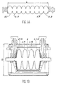
- Figure 1A shows a structure accelerator of an electron accelerator.
- Such a structure comes in the form of cells of successive cavities 2-1, .... 2-9.
- the particles are there accelerated by a radiofrequency wave generated by a klystron
- the length L is 1039 mm for a frequency of 1.3 GHz.
- Figure 1B shows a structure proton accelerator.
- Cells 2-10, ..., 2-13 in niobium are immersed in a bath of helium liquid.
- Such a structure has a diameter D of 1.1 m for a frequency of 700 MHz.
- a current j induces in the walls of the cavity leads to a loss of power high frequency.
- the LONDON layer a thin layer of superconducting material.
- the typical thickness of the LONDON layer is about 100 nm and does not depend on the frequency, as is the case for currents induced in a normal conductor.
- This dissipated energy makes it possible to explain the variations of the characteristic curve of a superconducting cavity Q (E acc ), or quality factor, as a function of the accelerating field. As the dissipated energy increases with the accelerating field, the characteristic curve follows a downward slope depending on the field.
- resistance BCS resistance BCS
- FIG. 2A An example of such a stiffened structure is illustrated in Figure 2A.
- a corrugated tube 4 is made with a high thickness of superconducting material, usually niobium, which is expensive.
- the tube is an assembly of elementary parts 5, 7, 9, 11 assembled by welds 6, 8, 10.
- FIG. 2B Another known structure, represented schematically in FIG. 2B, consists in producing cavity portions made of material 12 of medium thickness, soldering them together by welding seams 16 and to strengthen them by a ring 14 at the height of the irises (regions or areas of the smallest diameter).
- a ring 14 at the height of the irises (regions or areas of the smallest diameter).
- FIG. 2C Another technique (FIG. 2C) consists in depositing a thin layer 22 of niobium on a thick copper substrate 20.
- This method makes it possible to solve the problem of stiffening the structure.
- the resulting structure has limitations in terms of accelerator field that can be achieved. Indeed, for reasons related to the structure of the niobium superconducting layer deposited by "sputtering" on the copper substrate, the maximum electric fields likely to be reached remain of the order of 10 MV / m. For other machines, and in particular e + -e - colliders, this field is clearly insufficient.
- this heat as well produced at the inner wall of the cavity should be evacuated, as effectively as possible, to the helium bath, so as to limit the rise in temperature of the inner wall of the cavity.
- a “quench” or “thermal breakdown” generally starts in an area where there is more strong resistance, or a zone of “non conduction", or a defect or foreign particle on the surface of the superconducting material.
- the zone sees its temperature increase and tend towards a conductivity zone "not supra", which then extends until the all the energy stored in the cavity is dissipated in the hot region.
- the power density generated by the currents in the LONDON layer is proportional to the square of the local magnetic field B s .
- the value of the local magnetic field B (s), along the meridian, presents a maximum value obtained at the equator (zone of larger diameter).
- B s fades slowly, then more rapidly when the equator passes the iris.
- a defect will therefore not have the same harmfulness if is located at the equator, or if it is located very far from the equator, towards the iris.
- the area of the equator is particularly sensitive from the point of view of superconductivity defects since the currents of Foucault induced at the level of normal electrons, in internal skin, will be in this area larger than the makes the strong value of the magnetic field.
- the "harmfulness" of a defect is not identical according to its geographical location in the cavity. All things being equal, located at near the equator, in an area where the field magnetic is maximal, it will tend to present more harmful to the "quench” than if is located near the iris.
- niobium is hungry for oxygen, it takes a very good vacuum in the enclosure, when one performs the electron beam welding. of the Studies have shown that during the welding process, the bath of molten metal absorbed oxygen from the enclosure and thus created locally an area where the purity of niobium was degraded.
- the current structures implement a lot of welds, and these areas are particularly critical, especially those located in equator level.
- the welding techniques used tend to focus inwards (where is localized layer of LONDON) the impurities that increase, among others, the residual resistance.
- the known structures require the use of high purity materials having high thermal conductivity (corresponding to an RRR not less than 200), that is to say materials whose purification cost is added to the usual cost of materials standards (RRR, or "Residual Resistance Ratio ", is a measure of the purity of the material, involving structural defects and microscopic or macroscopic impurities. he is also defined by the ratio of resistivity Electric cold and temperature resistivity ambient).
- niobium even if uses high purity niobium, it should be noted that the thermal conductivity of this material is not very good compared, for example, to that of copper or aluminum. Moreover, in the case where the flow of heat created by a hot spot can not be absorbed in the thickness of niobium, it should be noted that the niobium / liquid helium interfacial resistance is not not negligible.
- JP-0 2220399 and JP-0 2220400 propose a technique of particular realization of cavities superconducting niobium whose walls are covered with a good thermal conductive metal at by means of a plasma spray application method.
- the rigidity of a cavity with a multi-cell structure can to be increased by welding stiffeners in the form of rings ( Figure 2B).
- An object of the present invention is to propose an accelerator cavity and a manufacturing method of such a cavity to solve the problems outlined above.
- one aim is to propose such a accelerator cavity with excellent thermal properties and mechanical rigidity and which either a particularly low realization cost.
- the rigidity of the cavity can certainly be increased by applying a layer of projected metal by thicker plasma.
- a layer of projected metal by thicker plasma.
- the realization of a thick metal layer, besides the cost it represents proves to be complex and long, given plasma projection conditions.
- the invention more precisely relates to a cavity Multi-Cell Particle Accelerator rosary, the cells presenting a region of more large diameter, called Equator region and regions end of smaller diameter called iris which connect the cells, the cells being delimited by a wall made of a material having superconducting properties, which is covered with least one layer of thermal conductive material, characterized in that the layer of conductive material thermal density has a greater thickness in the iris regions only in the Equator region of the cells.
- the lower thickness of conductive material thermal in the equator regions is not detrimental to rigidity.
- a quantity of thermal conductive material weaker can be implemented and the time application of this material can be reduced. The manufacturing costs of the cavity are found reduced.
- the thickness of the superconducting material can also be reduced. This further contributes to lower costs.
- a cavity according to the invention can be implementation especially for accelerators of electrons or protons.
- the material thermal conductor can be formed by projection plasma.
- Plasma projection makes it possible to obtain porous structure providing an interface whose total developed area may be larger than that obtained in the prior art. This increase of the exchange surface makes it possible to improve exchanges thermals between liquid helium and the source possible heat that could develop from local way.
- the increase of the exchange surface between materials can reduce Kapitza's resistance, or interfacial thermal resistance, which is one of physical properties that determine performance of the superconducting structure.
- the plasma spray coating process allows, depending on the size of the constituent particles powders, and according to the settings of the torch plasma, to obtain porous layers which can be adjust the porosity.
- the superconducting material is niobium
- the layer of conductive material thermal can be covered with a layer of a material with more acoustic impedance weak than that of the thermal conductive material.
- the cavity can be formed from a seamless tube that is deformed by a known method such as hydroforming, swaging, forming to hot, explosive forming, magnetoforming, ... Once got the tube with its ripples, instead of welding an outer ring, as in the prior art (FIG. 2B), the structure by externally projecting powder, by example of copper, on the outer surface.
- tungsten or any other material possessing good thermal characteristics.
- thermal conducting material is meant a material with good characteristics thermal devices to evacuate a "quench".
- the copper or tungsten are, for example, good candidates.
- the subject of the invention is also a method for producing an accelerator cavity comprising a plurality of cells with equator regions of larger diameter and more iris regions small diameter, and delimited by a wall in one material with superconducting properties, in which a layer of conductive material is formed on the surface of said wall by projection plasma.
- the thermal conductive material so as to form a thicker layer in the iris regions than in the equator regions.
- a method of making a cavity implements an element, for example a sheet or a thin tube made of a material superconductor, for example in niobium, thick less than or equal to 1 mm (for example: 0.5 mm, or a few tenths of a millimeter) that one seeks to stiffen by an outer coating.
- an element for example a sheet or a thin tube made of a material superconductor, for example in niobium, thick less than or equal to 1 mm (for example: 0.5 mm, or a few tenths of a millimeter) that one seeks to stiffen by an outer coating.
- a plasma projection on the outer surface of the element of superconducting material are by described in the article by M. DUCOS entitled “Thermal spray coating” appeared in Engineering Technique, volume M5, 1645, pages 1-23.
- the article by F. Brossa et al. Entitled “Plasma Spraying, A Versatile Coating Technique published in
- the resulting structure therefore includes the element chosen, for example a sheet, or a tube, covered of material that has been projected by plasma and that has the characteristics described in the article M. DUCOS quoted above (see in particular ⁇ 2.2 of this document).
- the coating presents some porosity. This is particularly the case for a coating of copper or tungsten deposited on a sheet or a thin tube of niobium. This porosity allows, in the case of an application to a cavity superconducting, more efficient cooling. In indeed, the cavity is immersed in a helium bath liquid and this, because of its properties, can easily enter the porosities of the deposited material. This results in more efficient cooling of the structure.
- the shape of the cavity allows it, it can be made from a seamless tube that deformed by a known method such as for example hydroforming, or hydroforming with buckling. We can also use hot forming or forming by explosion.
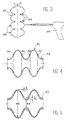
- Figure 3 shows a thin structure corrugated with niobium 30, on which a plasma spray coating using a torch, or a pistol, 32.
- a plasma torch, or pistol plasma is described in the article by M.
- DUCOS already Cited above.
- the cells each have a region of equator 46 of larger diameter and regions of iris 44 of smaller diameter.
- the iris regions 44 connect the cells.
- welds 34, 36, 38, 40 are not made at the level of equator regions but are deported from apart and else of the equator. According to the invention, the structure of Figure 4 is then intended to be externally coated with protection plasma, as described above.
- the projected material may be copper, or tungsten, or a mixture of powders or materials making it possible to produce a porous thermal layer.
- larger layers are deposited locally.
- the thickness of the layer (s) can vary continuously between the values L 1 and L 2 .
- L 1 and L 2 are adapted to the dimensions of the cavity. By way of example, values such as 1 mm ⁇ L 1 ⁇ L 2 ⁇ 5 mm may be indicated.
- the structure according to the invention makes it possible to obtain a stiffening, that is to say a mechanical reinforcement, of a superconducting structure.
- a stiffening that is to say a mechanical reinforcement
- the accelerator then has a tube having ripples, having the shape shown in FIG. 1A or 1B, this tube made of superconductor being reinforced by a layer of plasma deposited material as described above.
- the accelerator further comprises means for introduce a radiofrequency wave (a klystron), a liquid helium container, and the appropriate means to generate an accelerator electric field.
- the interfacial thermal resistance between two materials depends on the thermal coupling related to the acoustic phonons in the media located on either side of the interface.
- the thermal coupling is all the less good as there is acoustic mismatch between the two media.
- the phonon-related heat flux it can be shown that this depends, at an interface, on the exchange surface between the two interfaces. As the exchange surface increases, the heat flow increases.
- the coating structure according to the invention which makes it possible to produce a porous coating, thus having a large exchange surface, therefore makes it possible to improve the heat exchange between the element made of superconductive material, for example the tube, or the sheet, niobium, and its outer coating.
- the efficient flow of heat makes it possible to ensure a thermally stable operation of the cavity, without any appreciable deterioration of the HF characteristics, the accelerator electric fields E acc and the quality factor Q.
- a material that improves the resistance of Kapitza has, moreover, preferably a good thermal conductivity. This is the case of aluminum, but this is not the case for epoxy resins.
Landscapes
- Engineering & Computer Science (AREA)
- Physics & Mathematics (AREA)
- Plasma & Fusion (AREA)
- Spectroscopy & Molecular Physics (AREA)
- Thermal Sciences (AREA)
- Mechanical Engineering (AREA)
- General Engineering & Computer Science (AREA)
- Particle Accelerators (AREA)
Description

- Les figures 1A et 1B, déjà décrites, représentent des cavités supraconductrices connues, pour accélérateur d'électrons ou de protons.
- Les figures 2A à 2C, déjà décrites, représentent des structures supraconductrices connues, rigidifiées.
- La figure 3 représente un procédé de projection pas plasma d'un matériau pour la réalisation d'une cavité conforme à l'invention.
- La figure 4 représente une structure de cavité en niobium avec soudures déportées par rapport à l'équateur.
- La figure 5 représente une structure de cavité selon l'invention, avec revêtement d'épaisseur variable.
- la conductivité thermique λ en W/ mK,
- la chaleur spécifique volumique ρCv où ρ et Cv désignent respectivement la masse volumique et la chaleur spécifique à volume constant,
- la résistance thermique interfaciale entre matériaux, appelée aussi résistance de Kaptiza RK. Cette résistance traduit l'effet d'un saut de température, au niveau des interfaces, en présence d'un flux de chaleur. On peut aussi parler de conductibilité interfaciale hK (RK = 1 / hK).
Claims (10)
- Cavité d'accélérateur de particules à cellules multiples, dans lequel les cellules présentent une région de plus fort diamètre, appelée région d'équateur (46) et des régions d'extrémité de plus faible diamètre appelées régions d'iris (44) qui relient entre elles les cellules, les cellules étant délimitées par une paroi (30) en un matériau ayant des propriétés supraconductrices qui est recouverte d'au moins une couche de matériau conducteur thermique (45), caractérisée en ce que la couche de matériau conducteur thermique présente une épaisseur plus forte dans les régions d'iris que dans les régions d'équateur des cellules.
- Cavité selon la revendication 1, dans laquelle la couche de matériau conducteur thermique (45) présente une épaisseur qui varie continûment entre une première valeur L1 aux régions d'équateur (46) et une deuxième valeur L2 aux régions d'iris (44), la première valeur L1 étant inférieure à la deuxième valeur L2.
- Cavité selon la revendication 2, dans laquelle : 1 mm≤L1≤L2≤5 mm.
- Cavité selon la revendication 1, dans laquelle le matériau conducteur thermique présente une structure poreuse.
- Cavité selon la revendication 1, dans laquelle le matériau conducteur thermique est choisi parmi le cuivre, le tungstène ou un alliage progressif cuivre-aluminium.
- Cavité selon la revendication 1, dans laquelle la paroi (30) est formée d'une pluralité d'éléments assemblés par soudure (34-40).
- Cavité selon la revendication 1, dans laquelle la couche de matériau conducteur thermique (45) est recouverte d'une couche d'un matériau présentant une impédance acoustique plus faible que celle du matériau conducteur thermique.
- Cavité selon la revendication 1, dans lequel le matériau ayant des propriétés supraconductrices est du niobium.
- Procédé de réalisation d'une cavité d'accélérateur comprenant une pluralité de cellules avant des régions d'équateur (46) de plus fort diamètre et des régions d'iris (44), de plus faible diamètre, et délimitées par une paroi (30) en un matériau présentant des propriétés supraconductrices, dans lequel on forme une couche de matériau conducteur thermique (45) à la surface de ladite paroi par projection plasma, caractérisé en ce que l'on projette le matériau conducteur thermique de façon à former une couche plus épaisse dans les régions d'iris que dans les régions d'équateur.
- Procédé selon la revendication 9, dans lequel on forme un matériau conducteur thermique poreux.
Applications Claiming Priority (3)
| Application Number | Priority Date | Filing Date | Title |
|---|---|---|---|
| FR9712079A FR2769167B1 (fr) | 1997-09-29 | 1997-09-29 | Materiau supraconducteur renforce, cavite supraconductrice, et procedes de realisation |
| FR9712079 | 1997-09-29 | ||
| PCT/FR1998/002068 WO1999017592A1 (fr) | 1997-09-29 | 1998-09-28 | Materiau supraconducteur renforce, cavite supraconductrice, et procedes de realisation |
Publications (2)
| Publication Number | Publication Date |
|---|---|
| EP1020101A1 EP1020101A1 (fr) | 2000-07-19 |
| EP1020101B1 true EP1020101B1 (fr) | 2005-03-16 |
Family
ID=9511574
Family Applications (1)
| Application Number | Title | Priority Date | Filing Date |
|---|---|---|---|
| EP98946511A Expired - Lifetime EP1020101B1 (fr) | 1997-09-29 | 1998-09-28 | Cavite d'accelerateur de particules avec materiau supraconducteur renforce, et procede de realisation |
Country Status (5)
| Country | Link |
|---|---|
| US (1) | US6348757B1 (fr) |
| EP (1) | EP1020101B1 (fr) |
| DE (1) | DE69829396T2 (fr) |
| FR (1) | FR2769167B1 (fr) |
| WO (1) | WO1999017592A1 (fr) |
Families Citing this family (15)
| Publication number | Priority date | Publication date | Assignee | Title |
|---|---|---|---|---|
| RU2231235C2 (ru) * | 2001-12-06 | 2004-06-20 | Государственный научный центр РФ Институт физики высоких энергий | Способ изготовления сверхпроводящего резонатора |
| US7336764B2 (en) * | 2005-10-20 | 2008-02-26 | Agilent Technologies, Inc. | Electron beam accelerator and ceramic stage with electrically-conductive layer or coating therefor |
| JP2011167709A (ja) * | 2010-02-17 | 2011-09-01 | Mitsubishi Heavy Ind Ltd | 溶接方法および超伝導加速器 |
| JP5449093B2 (ja) * | 2010-09-03 | 2014-03-19 | 三菱重工業株式会社 | 超伝導加速空洞のポート部材 |
| CN103179775A (zh) * | 2013-02-28 | 2013-06-26 | 中国科学院高能物理研究所 | 超导加速器、用于超导加速器的超导腔及其制备方法 |
| ITMI20131508A1 (it) | 2013-09-11 | 2015-03-12 | Istituto Naz Di Fisica Nuclea Re | Metodo per aumentare il fattore di merito e il campo accelerante massimo in cavita' superconduttrici, cavita' superconduttrice realizzata secondo tale metodo e sistema per l'accelerazione di particelle utilizzante tale cavita'. |
| JP6049601B2 (ja) * | 2013-12-05 | 2016-12-21 | 三菱重工メカトロシステムズ株式会社 | 超伝導加速空洞、および超伝導加速空洞の電解研磨方法 |
| US9642239B2 (en) | 2015-04-17 | 2017-05-02 | Fermi Research Alliance, Llc | Conduction cooling systems for linear accelerator cavities |
| EP3385656B1 (fr) * | 2017-04-07 | 2020-09-16 | Karlsruher Institut für Technologie | Utilisation d'un couche sur une surface d'échangeur thermique |
| US10932355B2 (en) | 2017-09-26 | 2021-02-23 | Jefferson Science Associates, Llc | High-current conduction cooled superconducting radio-frequency cryomodule |
| US10856402B2 (en) * | 2018-05-18 | 2020-12-01 | Ii-Vi Delaware, Inc. | Superconducting resonating cavity with laser welded seam and method of formation thereof |
| CN110941882B (zh) * | 2019-10-17 | 2023-09-29 | 内蒙古科技大学 | 一种具有曲线界面的复合材料的热性能分析方法 |
| US12442583B2 (en) | 2020-05-12 | 2025-10-14 | Fermi Forward Discovery Group, Llc | Bolted joint conduction cooling apparatus for accelerator cavities |
| CN114371341B (zh) * | 2022-02-07 | 2025-04-04 | 北京高能锐新科技有限责任公司 | 用于超导腔的碗腔部件的测频设备 |
| CN114710872A (zh) * | 2022-03-29 | 2022-07-05 | 中国科学院近代物理研究所 | 一种可拆解的嵌套式复合超导腔 |
Family Cites Families (4)
| Publication number | Priority date | Publication date | Assignee | Title |
|---|---|---|---|---|
| JPS62263956A (ja) * | 1986-05-08 | 1987-11-16 | Mitsubishi Heavy Ind Ltd | 二層構造中空容器の製造法 |
| JPH02220400A (ja) * | 1989-02-20 | 1990-09-03 | Furukawa Electric Co Ltd:The | 超伝導空洞の製造方法 |
| JPH02220399A (ja) * | 1989-02-20 | 1990-09-03 | Furukawa Electric Co Ltd:The | 超伝導空洞の製造方法 |
| DE4138769A1 (de) * | 1991-11-26 | 1993-05-27 | Helmut Prof Dr Wipf | Vorrichtung und verfahren zur verbesserung des guetefaktors von niobhohlraumresonatoren |
-
1997
- 1997-09-29 FR FR9712079A patent/FR2769167B1/fr not_active Expired - Lifetime
-
1998
- 1998-09-28 DE DE69829396T patent/DE69829396T2/de not_active Expired - Lifetime
- 1998-09-28 EP EP98946511A patent/EP1020101B1/fr not_active Expired - Lifetime
- 1998-09-28 WO PCT/FR1998/002068 patent/WO1999017592A1/fr not_active Ceased
- 1998-11-29 US US09/508,693 patent/US6348757B1/en not_active Expired - Lifetime
Also Published As
| Publication number | Publication date |
|---|---|
| DE69829396T2 (de) | 2006-04-13 |
| WO1999017592A1 (fr) | 1999-04-08 |
| US6348757B1 (en) | 2002-02-19 |
| DE69829396D1 (de) | 2005-04-21 |
| FR2769167B1 (fr) | 1999-12-17 |
| EP1020101A1 (fr) | 2000-07-19 |
| FR2769167A1 (fr) | 1999-04-02 |
Similar Documents
| Publication | Publication Date | Title |
|---|---|---|
| EP1020101B1 (fr) | Cavite d'accelerateur de particules avec materiau supraconducteur renforce, et procede de realisation | |
| Padamsee | The science and technology of superconducting cavities for accelerators | |
| Sämann et al. | Laser porosificated silicon anodes for lithium ion batteries | |
| Zhang et al. | Development and vertical tests of a 166.6 MHz proof-of-principle superconducting quarter-wave beta= 1 cavity | |
| Proch | Superconducting cavities for accelerators | |
| CH642781A5 (fr) | Ensemble de fenetre a micro-onde et tube a micro-onde muni d'un tel ensemble. | |
| US7746192B2 (en) | Polyhedral contoured microwave cavities | |
| EP3098889B1 (fr) | Dispositif d'amenée de courant électrique sur un électrolyseur ou une pile à combustible haute température | |
| CN114727471A (zh) | 一种微波谐振腔 | |
| EP0499514B1 (fr) | Dispositif convertisseur de modes et diviseur de puissance pour tube hyperfréquence, et tube hyperfréquence comprenant un tel dispositif | |
| EP0117804B1 (fr) | Procédé de fabrication d'une cavité hyperfréquence, et cavité obtenue par ce procédé | |
| US3441880A (en) | High q radio frequency circuit employing a superconductive layer on a porous thermally matched substrate | |
| FR2873488A1 (fr) | FIL SUPRACONDUCTEUR A PHASE Nb-Sn ET PRECURSEUR POUR CE FIL | |
| EP2561521A1 (fr) | Bobine améliorée apte à générer un champ magnétique intense et procédé de fabrication de ladite bobine | |
| Ciovati | Superconducting radiofrequency cavities | |
| Grimm et al. | New directions in superconducting radio frequency cavities for accelerators | |
| FR2790595A1 (fr) | Circuit de ligne a retard en helice | |
| JP5544598B2 (ja) | 光陰極高周波電子銃、および光陰極高周波電子銃を備えた電子線装置 | |
| Posen et al. | SRF cavities beyond niobium: challenges and potential | |
| FR2551254A1 (fr) | Brins supraconducteurs utilisables aux frequences industrielles | |
| Simakov et al. | Raising gradient limitations in 2.1 GHz superconducting photonic band gap accelerator cavities | |
| GB2639908A (en) | Electromagnetic power source | |
| Benvenuti et al. | Various methods of manufacturing superconducting accelerating cavities | |
| Tiskumara | Nb3Sn Coating of Twin Axis Cavity and Other Complex SRF Cavity Structures | |
| Belomestnykh et al. | Design and first cold test of BNL superconducting 112 MHz QWR for electron gun applications |
Legal Events
| Date | Code | Title | Description |
|---|---|---|---|
| PUAI | Public reference made under article 153(3) epc to a published international application that has entered the european phase |
Free format text: ORIGINAL CODE: 0009012 |
|
| 17P | Request for examination filed |
Effective date: 20000331 |
|
| AK | Designated contracting states |
Kind code of ref document: A1 Designated state(s): DE FR GB IT |
|
| RTI1 | Title (correction) |
Free format text: PARTICLE ACCELERATOR CAVITY WITH REINFORCED SUPRACONDUCTIVE MATERIAL, AND METHOD FOR MAKING SAME |
|
| GRAP | Despatch of communication of intention to grant a patent |
Free format text: ORIGINAL CODE: EPIDOSNIGR1 |
|
| GRAS | Grant fee paid |
Free format text: ORIGINAL CODE: EPIDOSNIGR3 |
|
| GRAA | (expected) grant |
Free format text: ORIGINAL CODE: 0009210 |
|
| AK | Designated contracting states |
Kind code of ref document: B1 Designated state(s): DE FR GB IT |
|
| REG | Reference to a national code |
Ref country code: GB Ref legal event code: FG4D Free format text: NOT ENGLISH |
|
| REF | Corresponds to: |
Ref document number: 69829396 Country of ref document: DE Date of ref document: 20050421 Kind code of ref document: P |
|
| GBT | Gb: translation of ep patent filed (gb section 77(6)(a)/1977) |
Effective date: 20050607 |
|
| PLBE | No opposition filed within time limit |
Free format text: ORIGINAL CODE: 0009261 |
|
| STAA | Information on the status of an ep patent application or granted ep patent |
Free format text: STATUS: NO OPPOSITION FILED WITHIN TIME LIMIT |
|
| 26N | No opposition filed |
Effective date: 20051219 |
|
| REG | Reference to a national code |
Ref country code: FR Ref legal event code: PLFP Year of fee payment: 18 |
|
| REG | Reference to a national code |
Ref country code: FR Ref legal event code: PLFP Year of fee payment: 19 |
|
| REG | Reference to a national code |
Ref country code: FR Ref legal event code: PLFP Year of fee payment: 20 |
|
| PGFP | Annual fee paid to national office [announced via postgrant information from national office to epo] |
Ref country code: GB Payment date: 20170821 Year of fee payment: 20 Ref country code: FR Payment date: 20170822 Year of fee payment: 20 Ref country code: IT Payment date: 20170828 Year of fee payment: 20 Ref country code: DE Payment date: 20170821 Year of fee payment: 20 |
|
| REG | Reference to a national code |
Ref country code: DE Ref legal event code: R071 Ref document number: 69829396 Country of ref document: DE |
|
| REG | Reference to a national code |
Ref country code: GB Ref legal event code: PE20 Expiry date: 20180927 |
|
| PG25 | Lapsed in a contracting state [announced via postgrant information from national office to epo] |
Ref country code: GB Free format text: LAPSE BECAUSE OF EXPIRATION OF PROTECTION Effective date: 20180927 |