EP1020932A2 - PIN-Photodiode mit grosser Bandbreite - Google Patents
PIN-Photodiode mit grosser Bandbreite Download PDFInfo
- Publication number
- EP1020932A2 EP1020932A2 EP00300051A EP00300051A EP1020932A2 EP 1020932 A2 EP1020932 A2 EP 1020932A2 EP 00300051 A EP00300051 A EP 00300051A EP 00300051 A EP00300051 A EP 00300051A EP 1020932 A2 EP1020932 A2 EP 1020932A2
- Authority
- EP
- European Patent Office
- Prior art keywords
- region
- photodiode
- layer
- thickness
- approximately
- Prior art date
- Legal status (The legal status is an assumption and is not a legal conclusion. Google has not performed a legal analysis and makes no representation as to the accuracy of the status listed.)
- Withdrawn
Links
- 239000000872 buffer Substances 0.000 claims abstract description 52
- 230000007423 decrease Effects 0.000 claims abstract description 12
- 239000002019 doping agent Substances 0.000 claims abstract description 10
- GPXJNWSHGFTCBW-UHFFFAOYSA-N Indium phosphide Chemical compound [In]#P GPXJNWSHGFTCBW-UHFFFAOYSA-N 0.000 claims abstract description 9
- 238000000034 method Methods 0.000 claims description 6
- GYHNNYVSQQEPJS-UHFFFAOYSA-N Gallium Chemical compound [Ga] GYHNNYVSQQEPJS-UHFFFAOYSA-N 0.000 claims description 3
- 229910052733 gallium Inorganic materials 0.000 claims description 3
- 229910052738 indium Inorganic materials 0.000 claims description 3
- APFVFJFRJDLVQX-UHFFFAOYSA-N indium atom Chemical compound [In] APFVFJFRJDLVQX-UHFFFAOYSA-N 0.000 claims description 3
- 239000000758 substrate Substances 0.000 claims 2
- 230000003247 decreasing effect Effects 0.000 claims 1
- 229910000530 Gallium indium arsenide Inorganic materials 0.000 abstract 2
- KXNLCSXBJCPWGL-UHFFFAOYSA-N [Ga].[As].[In] Chemical compound [Ga].[As].[In] KXNLCSXBJCPWGL-UHFFFAOYSA-N 0.000 abstract 2
- 239000013307 optical fiber Substances 0.000 description 4
- 239000006117 anti-reflective coating Substances 0.000 description 3
- 238000009792 diffusion process Methods 0.000 description 3
- 230000003287 optical effect Effects 0.000 description 3
- 229910052581 Si3N4 Inorganic materials 0.000 description 2
- 229910004205 SiNX Inorganic materials 0.000 description 2
- 239000011248 coating agent Substances 0.000 description 2
- 238000000576 coating method Methods 0.000 description 2
- 229910052751 metal Inorganic materials 0.000 description 2
- 239000002184 metal Substances 0.000 description 2
- 150000002739 metals Chemical class 0.000 description 2
- 230000009467 reduction Effects 0.000 description 2
- 239000004065 semiconductor Substances 0.000 description 2
- HQVNEWCFYHHQES-UHFFFAOYSA-N silicon nitride Chemical compound N12[Si]34N5[Si]62N3[Si]51N64 HQVNEWCFYHHQES-UHFFFAOYSA-N 0.000 description 2
- NINIDFKCEFEMDL-UHFFFAOYSA-N Sulfur Chemical compound [S] NINIDFKCEFEMDL-UHFFFAOYSA-N 0.000 description 1
- 238000010521 absorption reaction Methods 0.000 description 1
- 230000004075 alteration Effects 0.000 description 1
- 230000004888 barrier function Effects 0.000 description 1
- 238000006243 chemical reaction Methods 0.000 description 1
- 239000000356 contaminant Substances 0.000 description 1
- 230000007613 environmental effect Effects 0.000 description 1
- 239000000835 fiber Substances 0.000 description 1
- QWXYZCJEXYQNEI-OSZHWHEXSA-N intermediate I Chemical compound COC(=O)[C@@]1(C=O)[C@H]2CC=[N+](C\C2=C\C)CCc2c1[nH]c1ccccc21 QWXYZCJEXYQNEI-OSZHWHEXSA-N 0.000 description 1
- 239000012464 large buffer Substances 0.000 description 1
- 238000004519 manufacturing process Methods 0.000 description 1
- 238000012986 modification Methods 0.000 description 1
- 230000004048 modification Effects 0.000 description 1
- 239000007787 solid Substances 0.000 description 1
- 229910052717 sulfur Inorganic materials 0.000 description 1
- 239000011593 sulfur Substances 0.000 description 1
- JBQYATWDVHIOAR-UHFFFAOYSA-N tellanylidenegermanium Chemical compound [Te]=[Ge] JBQYATWDVHIOAR-UHFFFAOYSA-N 0.000 description 1
Images



Classifications
-
- H—ELECTRICITY
- H10—SEMICONDUCTOR DEVICES; ELECTRIC SOLID-STATE DEVICES NOT OTHERWISE PROVIDED FOR
- H10F—INORGANIC SEMICONDUCTOR DEVICES SENSITIVE TO INFRARED RADIATION, LIGHT, ELECTROMAGNETIC RADIATION OF SHORTER WAVELENGTH OR CORPUSCULAR RADIATION
- H10F30/00—Individual radiation-sensitive semiconductor devices in which radiation controls the flow of current through the devices, e.g. photodetectors
- H10F30/20—Individual radiation-sensitive semiconductor devices in which radiation controls the flow of current through the devices, e.g. photodetectors the devices having potential barriers, e.g. phototransistors
- H10F30/21—Individual radiation-sensitive semiconductor devices in which radiation controls the flow of current through the devices, e.g. photodetectors the devices having potential barriers, e.g. phototransistors the devices being sensitive to infrared, visible or ultraviolet radiation
- H10F30/22—Individual radiation-sensitive semiconductor devices in which radiation controls the flow of current through the devices, e.g. photodetectors the devices having potential barriers, e.g. phototransistors the devices being sensitive to infrared, visible or ultraviolet radiation the devices having only one potential barrier, e.g. photodiodes
- H10F30/223—Individual radiation-sensitive semiconductor devices in which radiation controls the flow of current through the devices, e.g. photodetectors the devices having potential barriers, e.g. phototransistors the devices being sensitive to infrared, visible or ultraviolet radiation the devices having only one potential barrier, e.g. photodiodes the potential barrier being a PIN barrier
-
- H—ELECTRICITY
- H10—SEMICONDUCTOR DEVICES; ELECTRIC SOLID-STATE DEVICES NOT OTHERWISE PROVIDED FOR
- H10F—INORGANIC SEMICONDUCTOR DEVICES SENSITIVE TO INFRARED RADIATION, LIGHT, ELECTROMAGNETIC RADIATION OF SHORTER WAVELENGTH OR CORPUSCULAR RADIATION
- H10F77/00—Constructional details of devices covered by this subclass
- H10F77/10—Semiconductor bodies
- H10F77/12—Active materials
- H10F77/124—Active materials comprising only Group III-V materials, e.g. GaAs
-
- H—ELECTRICITY
- H10—SEMICONDUCTOR DEVICES; ELECTRIC SOLID-STATE DEVICES NOT OTHERWISE PROVIDED FOR
- H10F—INORGANIC SEMICONDUCTOR DEVICES SENSITIVE TO INFRARED RADIATION, LIGHT, ELECTROMAGNETIC RADIATION OF SHORTER WAVELENGTH OR CORPUSCULAR RADIATION
- H10F77/00—Constructional details of devices covered by this subclass
- H10F77/10—Semiconductor bodies
- H10F77/14—Shape of semiconductor bodies; Shapes, relative sizes or dispositions of semiconductor regions within semiconductor bodies
-
- Y—GENERAL TAGGING OF NEW TECHNOLOGICAL DEVELOPMENTS; GENERAL TAGGING OF CROSS-SECTIONAL TECHNOLOGIES SPANNING OVER SEVERAL SECTIONS OF THE IPC; TECHNICAL SUBJECTS COVERED BY FORMER USPC CROSS-REFERENCE ART COLLECTIONS [XRACs] AND DIGESTS
- Y02—TECHNOLOGIES OR APPLICATIONS FOR MITIGATION OR ADAPTATION AGAINST CLIMATE CHANGE
- Y02E—REDUCTION OF GREENHOUSE GAS [GHG] EMISSIONS, RELATED TO ENERGY GENERATION, TRANSMISSION OR DISTRIBUTION
- Y02E10/00—Energy generation through renewable energy sources
- Y02E10/50—Photovoltaic [PV] energy
- Y02E10/544—Solar cells from Group III-V materials
Definitions
- the invention relates generally to PIN photodiodes. More particularly, the invention relates PIN photodiodes having wide bandwidths.
- Fiber optic communications typically employ a modulated light source, such as a laser, a photodiode light detector, and an optical fiber interconnecting the laser and the photodiode.
- the laser typically is modulated to emit light pulses, which are to be received by remote photodiodes and converted into electrical signal outputs by the photodiodes.
- FIG. 1 shows a common PIN photodiode 10 of the prior art.
- the photodiode 10 is constructed as a chip having three semiconductor regions: a p region 12, an n region 14, and an intermediate i (intrinsic) region 16.
- the p and n regions 12 and 14 normally are doped to high carrier concentrations while the i region 16 typically is unintentionally doped to have a small, residual p or n type carrier concentration.
- a p contact 18, or anode is connected to the p region 12 and an n contact 20, or cathode, is connected to the n region 14.
- the p region 12 is coated with a dielectric coating 22 which prevents surface current leakage round the sides of the device and also serves as anti-reflective coating if the device is illuminated from the top side.
- the n region 14 is coated with an antireflective coating 24 which prevents reflection of the incident light away from the device.
- a thin buffer coating (not shown) on the order of 0.1 ⁇ m to 0.2 ⁇ m is placed between the n region 14 and the i region 16 to prevent diffusion therebetween and avoid inadvertent doping of the i region.
- PIN photodiodes such as that shown in Fig. 1 are negatively biased such that the entire i region 16 is depleted and substantially no current flows through the device under dark conditions.
- incident light for example light exiting an optical fiber, passes through either the transparent p region 12 or the transparent n region 14, it is absorbed by the i region 16 and the photons of light, hv, are converted into electron-hole pairs which create a net current flow through the photodiode 10.
- a high performance photodiode must meet the speed requirements of high-bit-rate systems and must be efficient in converting optical signals at the operating frequencies to electrical signal current.
- high-bit-rate systems typically operate in the 10 Ghz to 20 Ghz frequency range.
- the photodiode used must have an adequately wide bandwidth.
- the photodiode must be configured so as to minimize device capacitance.
- the capacitance of the pn junction, C j must be minimized.
- junction area minimization creates difficulties with optical fiber/photodiode alignment. Misalignment of the optical fiber with the photodiode can result in part or all of the optical signals not being absorbed in the i region of the photodiode, reducing the optical to electrical conversion efficiency and generating tails on the pulses resulting in a bandwidth reduction.
- W is another means of reducing capacitance. This normally is accomplished by increasing the thickness of the i region which, as mentioned above, typically is completely depleted by the negative bias applied to the photodiode. Although increasing i region thickness does effectively reduce capacitance of the photodiode, attempts to do so create manufacturing difficulties. In particular, it is difficult to grow relatively thick i regions composed of, for example, indium gallium phophide (InGaAs) with high yield results.
- InGaAs indium gallium phophide
- the present invention is a PIN photodiode comprising a p region containing a p type dopant, an n region containing an n type dopant, an i region positioned intermediate the p region and the n region, and a relatively thick, undoped buffer region positioned between the n region and the i region which substantially decreases the capacitance of the PIN photodiode such that the photodiode bandwidth is maximized.
- the buffer region is formed as a layer of indium phosphide that is at least approximately 0.5 ⁇ m in thickness. Most preferably, the buffer region has a thickness of approximately 0.5 ⁇ m to 2.5 ⁇ m, which is drastically greater than prior art buffer region thickness.
- the invention further relates to a method for increasing the bandwidth of a PIN photodiode comprising a p region, an n layer, and an i layer intermediate the p region and the n layer, comprising the step of providing a relatively thick, undoped buffer layer between the n layer and the i layer, wherein the buffer layer substantially decreases the capacitance of the PIN photodiode such that the photodiode bandwidth is maximized.
- Fig. 2 illustrates a PIN photodiode 100 constructed in accordance with the present invention.
- the photodiode 100 is formed as a semiconductor chip that comprises a p region 102, an n region 104, and an i region 106 that is intermediate the p and n regions 102 and 104.
- the i region 106 takes the form of a layer of indium gallium arsinide (InGaAs) that is approximately 1 ⁇ m to 6 ⁇ m thick.
- InGaAs indium gallium arsinide
- a cap layer 108 that prevents current leakage from the sides of the photodiode 100 and lowers contact resistance.
- the cap layer 108 typically is composed of indium phosphide (InP) or InGaAs and is approximately 0.25 ⁇ m to 1.5 ⁇ m thick.
- the p region 102 usually is formed in both the cap layer 108 and the i region 106 by diffusion with a p type dopant such as zinc (Zn).
- This p region 102 typically is approximately 0.35 ⁇ m to 3 ⁇ m in thickness and, together with the i region 106, forms a pn junction 110 that is approximately 12 ⁇ m to 500 ⁇ m in diameter.
- a dielectric layer 112 normally is provided over the cap layer 108 and a portion of the p region 102 as shown in Fig. 2.
- This dielectric layer 112 typically is composed of silicon nitride (SiN x ) and serves to reduce the amount of dark current that flows on the surface of the device as well as provide a barrier against environmental contaminants.
- Mounted to the top of the PIN photodiode 100 is a p contact 114, or anode, that is connected to the p region 102.
- the p contact 114 is composed of one or more highly electrically conductive metals.
- the n region 104 typically is formed as a layer of indium phosphide (InP) that contains an n type dopant such as sulfur (S). Normally, the n region is approximately 4 mils to 8mils in thickness and includes an integral lens 116 that is etched into the n region which focuses the incident light, hv, on the pn junction 110. It is to be understood, however, that the photodiode 100 of the present invention would function adequately without the provision of an integral lens such as that shown in Fig. 2.
- Mounted to the n region at the bottom of the device 100 is an n contact 118, or cathode, which is composed of one or more highly electrically conductive metals.
- the portion of the n region 104 not covered by the n contact 118, and therefore exposed to the incident light, hv, is covered with an antireflective coating 120 that typically is composed of silicon nitride (SiN x ).
- This buffer region 122 normally takes the form of a relatively thick undoped layer of indium phosphide (InP). Similar to the function of thin buffer layers used in some known PIN photodiodes, the buffer region 122 prevents inadvertent doping of the i region 106 caused by solid state diffusion between the n and i regions 104 and 106. Unlike such buffer layers, however, the relatively large thickness of the buffer region 122 serves to substantially decrease capacitance in the PIN photodiode and thereby substantially increase the photodiode bandwidth as is discussed hereinafter. In use, the buffer region 122 is depleted along with the i region 106 by the reverse bias applied to the photodiode 100.
- InP indium phosphide
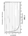
- Fig. 3 is a plot of the capacitance of a PIN photodiode having 2.9 ⁇ m thick i region as a function of buffer region thickness. As indicated in this plot, the capacitance of the photodiode decreases exponentially as the thickness of the buffer region is increased. As is further indicated by the plot, capacitance increases sharply when the buffer region is less than 0.5 ⁇ m (i.e., when the depletion region is less than 3.4 ⁇ m).
- the capacitance of the device decreases as the buffer region thickness increases, it would ostensibly be desirable to have a large buffer region 122, and therefore a large depletion region, W.
- increasing the thickness of the depletion region, W also increases transit time within the device.
- slow transit times delay the current output of the device to reduce bandwidth. Accordingly, it is desirable to select the thickness of the buffer region 122 to decrease capacitance without substantially increasing in transit time.
- Fig. 4 is a plot of photodiode bandwidth as a function of buffer region thickness. As indicated in this plot, the bandwidth is maximized, for a photodiode having an i region thickness of 2.9 ⁇ m, with buffer layer approximately 1.6 ⁇ m thick. Accordingly, maximum bandwidth is achieved when the depletion region, W, is approximately 4.5 ⁇ m thick (i.e., the sum of 2.9 ⁇ m and 1.6 ⁇ m). With reference again to Fig. 3, it can be appreciated that a buffer region thickness of approximately 1.6 ⁇ m results in greater than a factor of 3 decrease in capacitance as compared to conventional buffer layers on the order of 0.1 ⁇ m to 0.2 ⁇ m in thickness.
- the optimal buffer region 122 thickness may vary depending upon the thickness of the i region 106. Therefore, the thickness of the buffer region 122 can be varied when the thickness of the i region 106 is changed to maintain a constant thickness of the depletion region, W.
- the photodiode 100 is constructed with an i region 106 at least approximately 2.5 ⁇ m thick to ensure optimal absorption of the incident light, hv, and to maintain a quantum efficiency of at least 85%.
- the thickness of the i region 106 will not exceed approximately 3 ⁇ m since yield decreases significantly beyond that point and since quantum efficiency does not appreciably increase beyond that point.
- the buffer region 122 typically is approximately 0.5 ⁇ m to 2.5 ⁇ m in thickness. This range is considered preferable in that capacitance is likely to increase sharply when the buffer region thickness is below 0.5 ⁇ m, and since capacitance reduction levels off when the buffer region thickness exceeds 2.5 ⁇ m (see Fig. 3). As indicated in Fig. 4, this buffer region thickness range, for a PIN photodiode having an i region thickness of approximately 2.9 ⁇ m, results in a bandwidth greater than 8.5 GHz.
Landscapes
- Light Receiving Elements (AREA)
Applications Claiming Priority (2)
| Application Number | Priority Date | Filing Date | Title |
|---|---|---|---|
| US09/229,426 US6326649B1 (en) | 1999-01-13 | 1999-01-13 | Pin photodiode having a wide bandwidth |
| US229426 | 1999-01-13 |
Publications (2)
| Publication Number | Publication Date |
|---|---|
| EP1020932A2 true EP1020932A2 (de) | 2000-07-19 |
| EP1020932A3 EP1020932A3 (de) | 2001-11-14 |
Family
ID=22861200
Family Applications (1)
| Application Number | Title | Priority Date | Filing Date |
|---|---|---|---|
| EP00300051A Withdrawn EP1020932A3 (de) | 1999-01-13 | 2000-01-06 | PIN-Photodiode mit grosser Bandbreite |
Country Status (3)
| Country | Link |
|---|---|
| US (1) | US6326649B1 (de) |
| EP (1) | EP1020932A3 (de) |
| JP (1) | JP2000208807A (de) |
Cited By (1)
| Publication number | Priority date | Publication date | Assignee | Title |
|---|---|---|---|---|
| EP1198015A3 (de) * | 2000-09-13 | 2004-04-14 | TriQuint Technology Holding Co | Optoelektronische dotierte Vorrichtung zum Erhöhen der optischen Leistungsschwelle für den Bandbreiteeinsturz und Herstellungsverfahren |
Families Citing this family (51)
| Publication number | Priority date | Publication date | Assignee | Title |
|---|---|---|---|---|
| DE10024473B4 (de) * | 2000-05-18 | 2007-04-19 | Vishay Semiconductor Gmbh | Optischer Empfänger |
| US6724010B1 (en) * | 2000-08-03 | 2004-04-20 | General Electric Company | Solid state imager having gated photodiodes and method for making same |
| WO2002027874A2 (en) * | 2000-09-29 | 2002-04-04 | Cielo Communications, Inc. | High speed optical subassembly with ceramic carrier |
| JP2003249675A (ja) * | 2002-02-26 | 2003-09-05 | Sumitomo Electric Ind Ltd | 受光素子アレイ |
| US6815790B2 (en) * | 2003-01-10 | 2004-11-09 | Rapiscan, Inc. | Position sensing detector for the detection of light within two dimensions |
| US6727530B1 (en) * | 2003-03-04 | 2004-04-27 | Xindium Technologies, Inc. | Integrated photodetector and heterojunction bipolar transistors |
| US7655999B2 (en) | 2006-09-15 | 2010-02-02 | Udt Sensors, Inc. | High density photodiodes |
| US7279731B1 (en) * | 2006-05-15 | 2007-10-09 | Udt Sensors, Inc. | Edge illuminated photodiodes |
| US7256470B2 (en) | 2005-03-16 | 2007-08-14 | Udt Sensors, Inc. | Photodiode with controlled current leakage |
| US7656001B2 (en) * | 2006-11-01 | 2010-02-02 | Udt Sensors, Inc. | Front-side illuminated, back-side contact double-sided PN-junction photodiode arrays |
| US8164151B2 (en) * | 2007-05-07 | 2012-04-24 | Osi Optoelectronics, Inc. | Thin active layer fishbone photodiode and method of manufacturing the same |
| US7709921B2 (en) * | 2008-08-27 | 2010-05-04 | Udt Sensors, Inc. | Photodiode and photodiode array with improved performance characteristics |
| US7576369B2 (en) * | 2005-10-25 | 2009-08-18 | Udt Sensors, Inc. | Deep diffused thin photodiodes |
| US8035183B2 (en) * | 2003-05-05 | 2011-10-11 | Udt Sensors, Inc. | Photodiodes with PN junction on both front and back sides |
| US8120023B2 (en) * | 2006-06-05 | 2012-02-21 | Udt Sensors, Inc. | Low crosstalk, front-side illuminated, back-side contact photodiode array |
| US8686529B2 (en) * | 2010-01-19 | 2014-04-01 | Osi Optoelectronics, Inc. | Wavelength sensitive sensor photodiodes |
| US8519503B2 (en) * | 2006-06-05 | 2013-08-27 | Osi Optoelectronics, Inc. | High speed backside illuminated, front side contact photodiode array |
| US7880258B2 (en) * | 2003-05-05 | 2011-02-01 | Udt Sensors, Inc. | Thin wafer detectors with improved radiation damage and crosstalk characteristics |
| US7242069B2 (en) * | 2003-05-05 | 2007-07-10 | Udt Sensors, Inc. | Thin wafer detectors with improved radiation damage and crosstalk characteristics |
| US7057254B2 (en) * | 2003-05-05 | 2006-06-06 | Udt Sensors, Inc. | Front illuminated back side contact thin wafer detectors |
| US7049640B2 (en) * | 2004-06-30 | 2006-05-23 | The Boeing Company | Low capacitance avalanche photodiode |
| US9178092B2 (en) | 2006-11-01 | 2015-11-03 | Osi Optoelectronics, Inc. | Front-side illuminated, back-side contact double-sided PN-junction photodiode arrays |
| US20100053802A1 (en) * | 2008-08-27 | 2010-03-04 | Masaki Yamashita | Low Power Disk-Drive Motor Driver |
| US7759755B2 (en) | 2008-05-14 | 2010-07-20 | International Business Machines Corporation | Anti-reflection structures for CMOS image sensors |
| US8003425B2 (en) * | 2008-05-14 | 2011-08-23 | International Business Machines Corporation | Methods for forming anti-reflection structures for CMOS image sensors |
| US8546742B2 (en) * | 2009-06-04 | 2013-10-01 | Zena Technologies, Inc. | Array of nanowires in a single cavity with anti-reflective coating on substrate |
| US9515218B2 (en) | 2008-09-04 | 2016-12-06 | Zena Technologies, Inc. | Vertical pillar structured photovoltaic devices with mirrors and optical claddings |
| US8735797B2 (en) | 2009-12-08 | 2014-05-27 | Zena Technologies, Inc. | Nanowire photo-detector grown on a back-side illuminated image sensor |
| US8229255B2 (en) | 2008-09-04 | 2012-07-24 | Zena Technologies, Inc. | Optical waveguides in image sensors |
| US8889455B2 (en) | 2009-12-08 | 2014-11-18 | Zena Technologies, Inc. | Manufacturing nanowire photo-detector grown on a back-side illuminated image sensor |
| US8274039B2 (en) | 2008-11-13 | 2012-09-25 | Zena Technologies, Inc. | Vertical waveguides with various functionality on integrated circuits |
| US9478685B2 (en) | 2014-06-23 | 2016-10-25 | Zena Technologies, Inc. | Vertical pillar structured infrared detector and fabrication method for the same |
| US9082673B2 (en) | 2009-10-05 | 2015-07-14 | Zena Technologies, Inc. | Passivated upstanding nanostructures and methods of making the same |
| US8384007B2 (en) | 2009-10-07 | 2013-02-26 | Zena Technologies, Inc. | Nano wire based passive pixel image sensor |
| US9343490B2 (en) | 2013-08-09 | 2016-05-17 | Zena Technologies, Inc. | Nanowire structured color filter arrays and fabrication method of the same |
| US8835831B2 (en) | 2010-06-22 | 2014-09-16 | Zena Technologies, Inc. | Polarized light detecting device and fabrication methods of the same |
| US8791470B2 (en) | 2009-10-05 | 2014-07-29 | Zena Technologies, Inc. | Nano structured LEDs |
| US8748799B2 (en) | 2010-12-14 | 2014-06-10 | Zena Technologies, Inc. | Full color single pixel including doublet or quadruplet si nanowires for image sensors |
| US9299866B2 (en) | 2010-12-30 | 2016-03-29 | Zena Technologies, Inc. | Nanowire array based solar energy harvesting device |
| US8866065B2 (en) | 2010-12-13 | 2014-10-21 | Zena Technologies, Inc. | Nanowire arrays comprising fluorescent nanowires |
| US8269985B2 (en) | 2009-05-26 | 2012-09-18 | Zena Technologies, Inc. | Determination of optimal diameters for nanowires |
| US9000353B2 (en) | 2010-06-22 | 2015-04-07 | President And Fellows Of Harvard College | Light absorption and filtering properties of vertically oriented semiconductor nano wires |
| US9406709B2 (en) | 2010-06-22 | 2016-08-02 | President And Fellows Of Harvard College | Methods for fabricating and using nanowires |
| US8299472B2 (en) | 2009-12-08 | 2012-10-30 | Young-June Yu | Active pixel sensor with nanowire structured photodetectors |
| US8507840B2 (en) | 2010-12-21 | 2013-08-13 | Zena Technologies, Inc. | Vertically structured passive pixel arrays and methods for fabricating the same |
| US8890271B2 (en) | 2010-06-30 | 2014-11-18 | Zena Technologies, Inc. | Silicon nitride light pipes for image sensors |
| US8519379B2 (en) | 2009-12-08 | 2013-08-27 | Zena Technologies, Inc. | Nanowire structured photodiode with a surrounding epitaxially grown P or N layer |
| EP2335288A4 (de) * | 2008-09-15 | 2013-07-17 | Osi Optoelectronics Inc | Fischgräten-fotodiode mit dünner aktiver schicht und flacher n+-schicht sowie herstellungsverfahren dafür |
| US8072041B2 (en) * | 2009-04-08 | 2011-12-06 | Finisar Corporation | Passivated optical detectors with full protection layer |
| US8399909B2 (en) | 2009-05-12 | 2013-03-19 | Osi Optoelectronics, Inc. | Tetra-lateral position sensing detector |
| US8912615B2 (en) | 2013-01-24 | 2014-12-16 | Osi Optoelectronics, Inc. | Shallow junction photodiode for detecting short wavelength light |
Family Cites Families (15)
| Publication number | Priority date | Publication date | Assignee | Title |
|---|---|---|---|---|
| US4183034A (en) | 1978-04-17 | 1980-01-08 | International Business Machines Corp. | Pin photodiode and integrated circuit including same |
| US4885622A (en) | 1984-03-23 | 1989-12-05 | Oki Electric Industry Co., Ltd. | Pin photodiode and method of fabrication of the same |
| JPS61172381A (ja) * | 1984-12-22 | 1986-08-04 | Fujitsu Ltd | InP系化合物半導体装置 |
| FR2581482B1 (fr) | 1985-05-03 | 1987-07-10 | Labo Electronique Physique | Photodiode pin a faible courant de fuite |
| FR2597662B1 (fr) | 1986-04-22 | 1988-06-17 | Thomson Csf | Photodiode pin realisee a partir de semi-conducteur amorphe |
| US4794439A (en) * | 1987-03-19 | 1988-12-27 | General Electric Company | Rear entry photodiode with three contacts |
| US5252852A (en) * | 1989-03-14 | 1993-10-12 | Fujitsu Limited | Semiconductor device having flip chip bonding pads matched with pin photodiodes in a symmetrical layout configuration |
| US5528071A (en) | 1990-01-18 | 1996-06-18 | Russell; Jimmie L. | P-I-N photodiode with transparent conductor n+layer |
| JPH04111477A (ja) * | 1990-08-31 | 1992-04-13 | Sumitomo Electric Ind Ltd | 受光素子 |
| JPH04111479A (ja) * | 1990-08-31 | 1992-04-13 | Sumitomo Electric Ind Ltd | 受光素子 |
| US5045908A (en) | 1990-09-25 | 1991-09-03 | Motorola, Inc. | Vertically and laterally illuminated p-i-n photodiode |
| JP3292894B2 (ja) * | 1993-05-12 | 2002-06-17 | 日本電信電話株式会社 | 集積化受光回路 |
| IT1277856B1 (it) * | 1995-02-09 | 1997-11-12 | Univ Roma | Rivelatore di radiazione ultravioletta in film sottile, con opzione di elevata selettivita' spettrale. |
| US5818096A (en) | 1996-04-05 | 1998-10-06 | Nippon Telegraph And Telephone Corp. | Pin photodiode with improved frequency response and saturation output |
| DE19613820A1 (de) * | 1996-04-09 | 1997-10-23 | Forschungszentrum Juelich Gmbh | Struktur mit einer pin- oder nip-Schichtenfolge |
-
1999
- 1999-01-13 US US09/229,426 patent/US6326649B1/en not_active Expired - Fee Related
-
2000
- 2000-01-06 EP EP00300051A patent/EP1020932A3/de not_active Withdrawn
- 2000-01-13 JP JP4639A patent/JP2000208807A/ja active Pending
Cited By (1)
| Publication number | Priority date | Publication date | Assignee | Title |
|---|---|---|---|---|
| EP1198015A3 (de) * | 2000-09-13 | 2004-04-14 | TriQuint Technology Holding Co | Optoelektronische dotierte Vorrichtung zum Erhöhen der optischen Leistungsschwelle für den Bandbreiteeinsturz und Herstellungsverfahren |
Also Published As
| Publication number | Publication date |
|---|---|
| JP2000208807A (ja) | 2000-07-28 |
| US6326649B1 (en) | 2001-12-04 |
| EP1020932A3 (de) | 2001-11-14 |
Similar Documents
| Publication | Publication Date | Title |
|---|---|---|
| US6326649B1 (en) | Pin photodiode having a wide bandwidth | |
| US4493113A (en) | Bidirectional fiber optic transmission systems and photodiodes for use in such systems | |
| US7067853B1 (en) | Image intensifier using high-sensitivity high-resolution photodetector array | |
| US6104047A (en) | Avalanche photodiode with thin built-in depletion region | |
| US5365101A (en) | Photo-sensing device | |
| US6737718B2 (en) | Semiconductor photodetector | |
| US4577209A (en) | Photodiodes having a hole extending therethrough | |
| US20050017317A1 (en) | Doped absorption for enhanced responsivity for high speed photodiodes | |
| EP0532025B1 (de) | Optische Halbleitervorrichtung mit einem Halbleiterlaser und einem Photodetektor | |
| Chen et al. | A 2.5 Gbps CMOS fully integrated optical receicer with lateral PIN detector | |
| EP0181391B1 (de) | Rückbeleuchtete fotodiode mit einer frontschicht weiten bandabstandes | |
| Berger | MSM photodiodes | |
| US5594237A (en) | PIN detector having improved linear response | |
| US4587544A (en) | Avalanche photodetector | |
| US20110140168A1 (en) | Avalanche phototector with integrated micro lens | |
| US7368750B2 (en) | Semiconductor light-receiving device | |
| JPH04111478A (ja) | 受光素子 | |
| US4586067A (en) | Photodetector with isolated avalanche region | |
| EP1204148A2 (de) | Verbesserter flacher Photodetektor mit einem Resonanzhohlraum | |
| KR20010079915A (ko) | 고속 정면 조사형 포토 다이오드용의 고도화 도핑된 p형접점 | |
| JPH04246868A (ja) | P−i−nフォトダイオードおよびその効率を改善する方法 | |
| US4894703A (en) | Restricted contact, planar photodiode | |
| US4586066A (en) | Avalanche photodetector | |
| US4990989A (en) | Restricted contact planar photodiode | |
| JPH04263475A (ja) | 半導体受光素子及びその製造方法 |
Legal Events
| Date | Code | Title | Description |
|---|---|---|---|
| PUAI | Public reference made under article 153(3) epc to a published international application that has entered the european phase |
Free format text: ORIGINAL CODE: 0009012 |
|
| AK | Designated contracting states |
Kind code of ref document: A2 Designated state(s): AT BE CH CY DE DK ES FI FR GB GR IE IT LI LU MC NL PT SE Kind code of ref document: A2 Designated state(s): DE FR GB |
|
| AX | Request for extension of the european patent |
Free format text: AL;LT;LV;MK;RO;SI |
|
| RIN1 | Information on inventor provided before grant (corrected) |
Inventor name: FRAHM, ROBERT EUGENE Inventor name: ZOLNOWSKI, DENNIS RONALD Inventor name: LEE, KEON M. Inventor name: CHANG, CHIA C. Inventor name: LORIMOR, ORVAL GEORGE |
|
| 17P | Request for examination filed |
Effective date: 20010110 |
|
| RAP1 | Party data changed (applicant data changed or rights of an application transferred) |
Owner name: AGERE SYSTEMS OPTOELECTRONICS GUARDIAN CORPORATION |
|
| PUAL | Search report despatched |
Free format text: ORIGINAL CODE: 0009013 |
|
| AK | Designated contracting states |
Kind code of ref document: A3 Designated state(s): AT BE CH CY DE DK ES FI FR GB GR IE IT LI LU MC NL PT SE |
|
| AX | Request for extension of the european patent |
Free format text: AL;LT;LV;MK;RO;SI |
|
| AKX | Designation fees paid |
Free format text: DE FR GB |
|
| 17Q | First examination report despatched |
Effective date: 20021030 |
|
| STAA | Information on the status of an ep patent application or granted ep patent |
Free format text: STATUS: THE APPLICATION IS DEEMED TO BE WITHDRAWN |
|
| 18D | Application deemed to be withdrawn |
Effective date: 20030510 |