EP1022820A2 - Dispositif de contacts pour des connecteurs à jack modulaires - Google Patents
Dispositif de contacts pour des connecteurs à jack modulaires Download PDFInfo
- Publication number
- EP1022820A2 EP1022820A2 EP00200241A EP00200241A EP1022820A2 EP 1022820 A2 EP1022820 A2 EP 1022820A2 EP 00200241 A EP00200241 A EP 00200241A EP 00200241 A EP00200241 A EP 00200241A EP 1022820 A2 EP1022820 A2 EP 1022820A2
- Authority
- EP
- European Patent Office
- Prior art keywords
- contact
- jack
- modular
- male
- mating portion
- Prior art date
- Legal status (The legal status is an assumption and is not a legal conclusion. Google has not performed a legal analysis and makes no representation as to the accuracy of the status listed.)
- Granted
Links
Images


Classifications
-
- H—ELECTRICITY
- H01—ELECTRIC ELEMENTS
- H01R—ELECTRICALLY-CONDUCTIVE CONNECTIONS; STRUCTURAL ASSOCIATIONS OF A PLURALITY OF MUTUALLY-INSULATED ELECTRICAL CONNECTING ELEMENTS; COUPLING DEVICES; CURRENT COLLECTORS
- H01R24/00—Two-part coupling devices, or either of their cooperating parts, characterised by their overall structure
- H01R24/60—Contacts spaced along planar side wall transverse to longitudinal axis of engagement
- H01R24/62—Sliding engagements with one side only, e.g. modular jack coupling devices
- H01R24/64—Sliding engagements with one side only, e.g. modular jack coupling devices for high frequency, e.g. RJ 45
Definitions
- the present invention relates to electrical connectors and, more particularly, is directed toward an improved contact design to be used in modular telephone-style jacks so that during mating, the contact has a bi-directional means of transferring vertical lift by a modular plug into both vertical and horizontal direction.
- Telephone-style modular jacks are widely used in the computer networking and communications industries for interconnection of computers, modems, printers, and similar electronic equipment.
- module jack and “modular plug” connote the miniature, interchangeable, quick-connect-and-disconnect jacks and plugs developed originally by Western Electric Company and Belt Telephone Laboratories. Examples of modular jacks and modular plugs may be seen as described in US Patent numbers 3,699,498: 3,850,497; and 3,860,316.
- the four types of plugs are essentially identical in their dimensions in the critical inter-mating front portion except that the width of the six position plug is 0.080 inches wider than the four position plug, and the width of the eight and ten position plugs are 0.080 inches wider than the six position plug.
- This design arrangement permits any plug to be mateably inserted into any jack of the same number position or any jack of a greater number position. For example, this means that a four position plug can be inserted into a four position jack, or a six position jack, or an eight position jack, or a ten position jack. Another example would be that a six position plug could be inserted into a six position jack, or an eight position jack.
- U.S. Patent number 5,478,261 is designed to address this very serious potential type of field induced failure of a modular jack.
- An intermediate, transition portion of the contact joins the contact mating portion and joins the solder post portion of the spring contact.
- the contact mating portion is comprised of several sections: the lower linear beam, the lead-in, the forward tip, and the back angle section.
- the transition portion of the contact extends typically in a vertical fashion from the solder posts up to a radius directional changer, from which the transition portion typically extends horizontally forwardly toward the front face of the jack.
- the back angle-up connects to the transition portion and extends downwardly from the transition portion to connect to the lower linear beam.
- the back angle section enables the lower linear beam to be positioned within the jack so that its beam surface is lower than the horizontal part of the transition portion.
- the lead-in angles upward from the lower linear beam to the forward tip.
- the combination of lead-in section with the back angle section makes it possible to locate the mating beam surface relatively far away from the points of flexure for the contact, reducing the effects of the contact being lifted to a high lifted position, the source of excessive stress on the contacts of a modular jack.
- the beam surface when lifted to normal lift height while mated, becomes parallel to the upper surface of the male contact in the plug. This dramatically improves the electrical properties of the connector as will be described hereinafter.
- prior art jacks typically have a VSWR of greater than 2.0 with signals transmitted at a frequency of 100 Mbps, while my '5,478,261 jack provides a VSWR of 1.1 at a frequency of 100 Mbps.
- My '5,478,261 jack reflects away less than 5% of the transmitted signal, providing for more than 95% of the original signal to continue on.
- US Patent number 5,249,987 illustrates a further improvement to the design of US Patent 5,478,261 by providing a flexible cover located within the upper wall of the jack.
- This cover is designed to provide a dielectric barrier between the spring contacts and any external electrically charged surface or electrically conductive surface.
- the cover is made of polymers that have some flexibility in thin sections, thereby providing support for spring contacts which are lifted to a high lift position, and additionally providing for continuing dielectric isolation for the now lifted contacts. The cover will lift in concert with the spring contacts that are lifted such that it lifts equally to those spring contacts which experience the highest lift.
- This improved jack still has a disadvantage in that in space limited computers, network boxes, and the like, there is not sufficient headroom above the upper wall of the jack for the spring contacts and the cover to flex to their fully unrestrained position when a smaller position plug is mated and specific contacts are lifted to a high lift position.
- a primary object of the present invention is to provide a modular female jack with an enhanced contact shape and design that utilizes a highly stress resistant contact design and a glide dimple to further improve stress resistance to overcome the deficiencies of the prior art.
- Another object of the present invention is to provide a means for the spring contact of the jack to move in both a vertical direction and in a horizontal direction.
- a further object of the present invention is to provide a spring contact having a dimple that can move with relative ease across a surface of a jack or a cover for the jack.
- Yet another object of the present invention is to provide a means for the spring contact to primarily lift in a vertical fashion prior to extending itself in a horizontal fashion
- a spring contact consisting of a contact mating portion, a transfer portion, a solder tail portion, and a transition portion.
- the transfer portion is located forwardly of the contact mating portion so that it can serve as a point of leverage for the spring contact.
- the contact mating portion is comprised of a lower linear beam, a back-angle section, a lead-in section in which the lower linear beam occupies a lower relative position within the jack than the horizontal part of the transition portion.
- the transfer portion is forward of the lead-in section and has the shape of an arc whose open side faces the bottom of the jack.
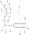
- FIG 1 a preferred embodiment of the present invention is indicated generally by reference numeral 70.
- the female spring contact 70 is comprised of four portions, each integrally joined with at least one other portion so that taken together, they define a unique contact design and shape.
- the transfer portion 20 consists of two sections, the tip 24, and the transfer dimple 22.
- Contact mating portion 10 consists of three sections, the lower linear beam 12, the back-angle 14, and the lead-in 16.
- Transition portion consists of a substantially horizontal section 32, a radius directional changer 34, and a substantially vertical section 36.
- Solder tail portion consists of a spreader section and solder post 42 or 44.
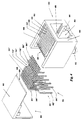
- Tip 24 is designed to hold the contact mating portion in a stable, controlled position relative to jack housing 80 (Fig 3) by providing a surface that rests on the upper surface of an internal ledge (not shown) adjacent the front wall 84 of housing 80.
- the internal ledge is located below the top edges of separator(s) 54 and within the housing 80 just behind the top edge of front wall 84.
- guide dimple 22 Located adjacent tip 24 is guide dimple 22, having an arcuate shape disposed such that the open side of the arc faces away from the upper surface of connector 80. This provides a curved, smooth, burr free surface designed to move across the underside 64 of cover 60.
- the uppermost point of glide dimple 22 makes tangential contact with underside 64, resulting in a relatively low resistance by the cover 60 to move of glide dimple 22 across the surface of underside 64.
- Contact mating portion 10 is comprised of lead-in 16, which has an angular orientation relative to the front wall 84 of housing 80.
- This angular orientation allows the lead-in to engage the leading radius of a contact blade within a male plug so that the contact blade can gradually lift the contact mating portion as the contact blade of a plug moves in a direction toward the rear of the jack.
- This lifting action urges the lower linear beam 12 to lift so as to easily move onto the upper surface of a contact blade, resulting in a mated pair between the beam 12 and the upper surface of a contact blade.
- the back-angle 14 joins the lower linear beam to the transition portion 30, and more particularly, to the horizontal section 32 of the transition portion 30.
- Transition portion consists of horizontal section 32, which provides a long span from the back-angle section and the radius directional changer 34. Radius directional changer joins to vertical section 36 through a curved shape. This combination absorbs stress delivered to the long span horizontal section 32, which takes on a slight bow shape under contact lift, while part of the lift stress travels through curved shape of radius changer 34, and then into the vertical section 36.
- Solder tail portion 40 has solder post(s) 40, 42 which are designed to be inserted into plated thru holes in the printed circuit board.
- FIG. 2 An alternate embodiment of spring contact 70' is shown in Fig. 2, in which contact mating portion 10' and transfer portion 20' correspond respectively to contact mating portion 10 and transfer portion 20 of Fig 1. It maybe seen that lower linear beam 12' of Fig 2 is shorter in length than lower linear beam 12 of Fig 1, that lead-in 16' of Fig 2 has a greater angularity than lead-in 16 of Fig 1, that glide dimple 22' of Fig 2 has a larger arc than glide dimple 22 of Fig 1, and that tip 24' of Fig 2 is longer than tip 24 of Fig 1. These differences are the result of alternate spring contact 70' of Fig 2 having different functionality than spring contact 70 of Fig 1.
- spring contact 70' has a shortened lower linear beam 12' and a more angular lead-in 16' so that the internally exposed contact mating portion 10' is recessed farther from the front wall 84 of jack 80. This substantially reduces the likelihood of accidental contact with voltages on spring contacts 10' in jack 80. This is a highly desirable feature with a clear safety benefit to consumer users of modular jacks or equipment containing modular jacks.
- Front wall 84 contains an opening 82, which is of a shape and size to accept a modular male plug into the opening 82.
- Adjacent front face 84 are two catches 86, located at the entrance of opening 82. These catches 86 are designed to capture two corresponding projections on the latching arm of a modular male plug.
- Surfaces 85 provide a guide and support surface for a modular male plug to ride on as the male plug is inserted into opening 82 until the male plug latching arm projections snap into engagement behind catches 86.
- Open channels 52 and 56 are of a width and length to accept one spring contact in each channel 52, 56 such that the width of channel 52 and channel 56 are wider than the width of spring contact 70 for contact sections 32, 14, 12, 16, 22, and 24. This provides the means for each spring contact 70 to freely move within its corresponding contact channel. As a result, spring contact 70 can follow the movement of a plug as it is inserted into opening 82 as well as after a male plug is fully seated within opening 82.
- Cover support ledge 57 is located along the upper surface of connector 80, and extends from front wall 84 rearwardly, having a length approximately one-half of the front to rear depth of connector 80.
- Support ledge 57 provides a physical stop and resting surface for a recessed channel 66 on the underside of separable cover 60.
- the result of support ledge 57 is that it maintains accurate positioning of front overhang 62 of cover 60, so that cover 60 does not change the force applied by spring contact(s) 70 until spring contacts have been lifted high enough such that transfer dimple 22 engages underside 64 of cover 60.
- Support ledge 57, with the overlap of recessed channel 66 of cover 60, and the side surface alignment between upper edge(s) 58 and outer edges of overhang 62, provides a greater dielectric barrier to voltages arcing from spring contact(s) 70 to an external bracket or frame.
- Glide dimple 22 as mating contact portion 10 is lifted when a male plug is inserted into opening 82, lifts correspondingly so as to engage underside 64 of cover 60. As overhang 62 lifts from the engagement of lifting glide dimple 22, overhang 62 continues to lift unrestrained unless it encounters a fixed object or surface. Any such fixed object or surface will prevent further lifting of overhand 62, and correspondingly prevent any further lifting of glide dimple 22, thereby stopping further vertical movement of contact mating portion 10. This causes glide dimple 22 to begin to slide along underside 64 of overhand 62 in a direction toward front wall 84 of housing 80.
- contact mating portion 10 is compressed, causing tip 24 and glide dimple 22 to move and extend toward front wall 84, thereby absorbing the additional stress induced by high lifting of contact mating portion 10 and preventing permanent deformation of the contact mating portion 10.
- this permits the use of more rigid materials for the separable cover 60 so that cover 60 itself limits the amount of lift of spring contacts 70.
- Fig 4 illustrates an alternate embodiment of the present invention shown in perspective, exploded view.
- the connector housing 80, cover 60, and spring contact(s) 70' are assembled in a comparable process to that described for Fig 3, in which analogous prime numbers functionally correspond to similar number's functions as described in Fig 3.
Landscapes
- Coupling Device And Connection With Printed Circuit (AREA)
- Details Of Connecting Devices For Male And Female Coupling (AREA)
Applications Claiming Priority (2)
| Application Number | Priority Date | Filing Date | Title |
|---|---|---|---|
| US09/236,921 US6093059A (en) | 1999-01-25 | 1999-01-25 | Contact configuration in modular jack |
| US236921 | 1999-01-25 |
Publications (3)
| Publication Number | Publication Date |
|---|---|
| EP1022820A2 true EP1022820A2 (fr) | 2000-07-26 |
| EP1022820A3 EP1022820A3 (fr) | 2001-12-12 |
| EP1022820B1 EP1022820B1 (fr) | 2007-03-28 |
Family
ID=22891554
Family Applications (1)
| Application Number | Title | Priority Date | Filing Date |
|---|---|---|---|
| EP00200241A Expired - Lifetime EP1022820B1 (fr) | 1999-01-25 | 2000-01-21 | Dispositif de contacts pour des connecteurs à jack modulaires |
Country Status (5)
| Country | Link |
|---|---|
| US (1) | US6093059A (fr) |
| EP (1) | EP1022820B1 (fr) |
| JP (1) | JP4489226B2 (fr) |
| CA (1) | CA2291295C (fr) |
| DE (1) | DE60034082T2 (fr) |
Cited By (2)
| Publication number | Priority date | Publication date | Assignee | Title |
|---|---|---|---|---|
| WO2004102750A1 (fr) * | 2003-05-13 | 2004-11-25 | Molex Incorporated | Dispositif connecteur modulaire pour jacks a nombre variable de fils |
| EP3282525A1 (fr) * | 2011-04-20 | 2018-02-14 | CCS Technology Inc. | Connecteur électrique de type fiche |
Families Citing this family (10)
| Publication number | Priority date | Publication date | Assignee | Title |
|---|---|---|---|---|
| US6394850B1 (en) | 2000-03-20 | 2002-05-28 | David Oliphant | Contact pin design for a modular jack |
| US6650546B2 (en) | 2001-02-27 | 2003-11-18 | 3Com Corporation | Chip component assembly |
| US6554653B2 (en) | 2001-03-16 | 2003-04-29 | Adc Telecommunications, Inc. | Telecommunications connector with spring assembly and method for assembling |
| US6796847B2 (en) | 2002-10-21 | 2004-09-28 | Hubbell Incorporated | Electrical connector for telecommunications applications |
| US7052328B2 (en) | 2002-11-27 | 2006-05-30 | Panduit Corp. | Electronic connector and method of performing electronic connection |
| CA2550527A1 (fr) * | 2005-06-21 | 2006-12-21 | Ideal Industries, Inc. | Sectionneur electrique muni de connecteurs a enfoncer |
| US7527509B1 (en) * | 2005-06-21 | 2009-05-05 | Ideal Industries, Inc. | Electrical disconnect with push-in connectors |
| US7727002B2 (en) * | 2006-06-21 | 2010-06-01 | Ideal Industries, Inc. | Electrical disconnect with adjacent wire receptacle boxes |
| WO2014190238A1 (fr) | 2013-05-23 | 2014-11-27 | Rapid Diagnostek | Système de module de capteur à résonateur et procédé |
| US11476605B2 (en) | 2013-05-23 | 2022-10-18 | Qorvo Biotechnologies, Llc | Interconnect device and module using same |
Family Cites Families (10)
| Publication number | Priority date | Publication date | Assignee | Title |
|---|---|---|---|---|
| US3369214A (en) * | 1965-10-27 | 1968-02-13 | Bell Telephone Labor Inc | Connector |
| US5478261A (en) * | 1978-06-14 | 1995-12-26 | Virginia Patent Development Corp. | Modular jack for directly coupling modular plug with printed circuit board |
| US4566749A (en) * | 1984-08-09 | 1986-01-28 | Brand-Rex Company | Electrical connector receptacle |
| US5145398A (en) * | 1989-09-06 | 1992-09-08 | Amp Incorporated | Turning insertion type electrical connector system |
| US5064387A (en) * | 1990-06-12 | 1991-11-12 | Thomas & Betts Corporation | Shielded electrical jack connector |
| US5249987A (en) * | 1992-03-31 | 1993-10-05 | Virginia Patent Development Corporation | Cap for modular jack |
| EP0654865B1 (fr) * | 1993-10-27 | 1998-08-05 | Molex Incorporated | Connecteur électrique à dispositif de shuntage |
| US5639266A (en) * | 1994-01-11 | 1997-06-17 | Stewart Connector Systems, Inc. | High frequency electrical connector |
| US5704802A (en) * | 1996-06-14 | 1998-01-06 | Maxconn Incorporated | Modular jack assembly |
| US5702271A (en) * | 1996-08-30 | 1997-12-30 | The Whitaker Corporation | Ultra low profile board-mounted modular jack |
-
1999
- 1999-01-25 US US09/236,921 patent/US6093059A/en not_active Expired - Lifetime
- 1999-11-30 CA CA002291295A patent/CA2291295C/fr not_active Expired - Fee Related
-
2000
- 2000-01-21 EP EP00200241A patent/EP1022820B1/fr not_active Expired - Lifetime
- 2000-01-21 DE DE60034082T patent/DE60034082T2/de not_active Expired - Lifetime
- 2000-01-25 JP JP2000016158A patent/JP4489226B2/ja not_active Expired - Fee Related
Cited By (3)
| Publication number | Priority date | Publication date | Assignee | Title |
|---|---|---|---|---|
| WO2004102750A1 (fr) * | 2003-05-13 | 2004-11-25 | Molex Incorporated | Dispositif connecteur modulaire pour jacks a nombre variable de fils |
| CN100389525C (zh) * | 2003-05-13 | 2008-05-21 | 莫列斯公司 | 用于插入带多根引线丝的插头的模块插座组件 |
| EP3282525A1 (fr) * | 2011-04-20 | 2018-02-14 | CCS Technology Inc. | Connecteur électrique de type fiche |
Also Published As
| Publication number | Publication date |
|---|---|
| EP1022820A3 (fr) | 2001-12-12 |
| CA2291295C (fr) | 2004-04-13 |
| DE60034082T2 (de) | 2007-12-13 |
| US6093059A (en) | 2000-07-25 |
| EP1022820B1 (fr) | 2007-03-28 |
| CA2291295A1 (fr) | 2000-07-25 |
| JP4489226B2 (ja) | 2010-06-23 |
| JP2000223197A (ja) | 2000-08-11 |
| DE60034082D1 (de) | 2007-05-10 |
Similar Documents
| Publication | Publication Date | Title |
|---|---|---|
| US9178310B2 (en) | Duplex male electrical connector with a connection board movable inside a socket shell | |
| EP1022820B1 (fr) | Dispositif de contacts pour des connecteurs à jack modulaires | |
| EP1066663B1 (fr) | Connecteur electrique modulaire plat et carte de communication comprenant celui-ci | |
| US7985101B2 (en) | RJ-45 style communications jacks that are configured to receive both RJ-45 and RJ-11 style communications plugs | |
| US20150303623A1 (en) | Electrical receptacle connector and electrical plug connector | |
| US6183306B1 (en) | Staggered interface contacts | |
| CN112736535B (zh) | 一种电连接插座、光电模块、笼子及电子设备 | |
| JP2000215955A (ja) | 選択自在で互換性のある電気コネクタ・ジャック | |
| US6488543B2 (en) | Modular jack for type III PCMCIA cards | |
| US6354883B2 (en) | Connector with adjustable thickness | |
| EP1037314B1 (fr) | Ensemble de réceptacle et circuit imprimé servant à recevoir une fiche | |
| CN207199901U (zh) | 插座电连接器 | |
| EP1109268B1 (fr) | Jack modulaire avec membre de positionement pour fiche modulaire | |
| CN110998986A (zh) | 正反双面电连接器 | |
| US7140891B1 (en) | Dustproof receptacle connector | |
| US6155880A (en) | Wall-mounted receptacle adapter | |
| AU757677B2 (en) | Selectable compatibility electrical connector plug | |
| US7651343B2 (en) | Low profile electrical connector | |
| US7559775B2 (en) | Electrical card connector assembly | |
| US6333860B1 (en) | Emi shield with connector cover extension | |
| US20110256782A1 (en) | Electrical connector having movable central contact | |
| US20100255725A1 (en) | LVDS Connector | |
| CN202231235U (zh) | 具套接壳的双面电连接公头 | |
| CN109066143A (zh) | 一种高速传输电连接器插座 | |
| CN220042366U (zh) | 具有外弧结构的连接器及其壳体 |
Legal Events
| Date | Code | Title | Description |
|---|---|---|---|
| PUAI | Public reference made under article 153(3) epc to a published international application that has entered the european phase |
Free format text: ORIGINAL CODE: 0009012 |
|
| AK | Designated contracting states |
Kind code of ref document: A2 Designated state(s): AT BE CH LI Kind code of ref document: A2 Designated state(s): AT BE CH CY DE DK ES FI FR GB GR IE IT LI LU MC NL PT SE |
|
| AX | Request for extension of the european patent |
Free format text: AL;LT;LV;MK;RO;SI |
|
| PUAL | Search report despatched |
Free format text: ORIGINAL CODE: 0009013 |
|
| RAP1 | Party data changed (applicant data changed or rights of an application transferred) |
Owner name: THOMAS & BETTS INTERNATIONAL, INC. |
|
| AK | Designated contracting states |
Kind code of ref document: A3 Designated state(s): AT BE CH CY DE DK ES FI FR GB GR IE IT LI LU MC NL PT SE |
|
| AX | Request for extension of the european patent |
Free format text: AL;LT;LV;MK;RO;SI |
|
| 17P | Request for examination filed |
Effective date: 20020610 |
|
| AKX | Designation fees paid |
Free format text: AT BE CH LI |
|
| RBV | Designated contracting states (corrected) |
Designated state(s): DE FR GB |
|
| REG | Reference to a national code |
Ref country code: DE Ref legal event code: 8566 |
|
| GRAP | Despatch of communication of intention to grant a patent |
Free format text: ORIGINAL CODE: EPIDOSNIGR1 |
|
| GRAS | Grant fee paid |
Free format text: ORIGINAL CODE: EPIDOSNIGR3 |
|
| GRAA | (expected) grant |
Free format text: ORIGINAL CODE: 0009210 |
|
| AK | Designated contracting states |
Kind code of ref document: B1 Designated state(s): DE FR GB |
|
| REG | Reference to a national code |
Ref country code: GB Ref legal event code: FG4D |
|
| REF | Corresponds to: |
Ref document number: 60034082 Country of ref document: DE Date of ref document: 20070510 Kind code of ref document: P |
|
| ET | Fr: translation filed | ||
| PLBE | No opposition filed within time limit |
Free format text: ORIGINAL CODE: 0009261 |
|
| STAA | Information on the status of an ep patent application or granted ep patent |
Free format text: STATUS: NO OPPOSITION FILED WITHIN TIME LIMIT |
|
| 26N | No opposition filed |
Effective date: 20080102 |
|
| PGFP | Annual fee paid to national office [announced via postgrant information from national office to epo] |
Ref country code: DE Payment date: 20140129 Year of fee payment: 15 |
|
| PGFP | Annual fee paid to national office [announced via postgrant information from national office to epo] |
Ref country code: FR Payment date: 20140117 Year of fee payment: 15 |
|
| PGFP | Annual fee paid to national office [announced via postgrant information from national office to epo] |
Ref country code: GB Payment date: 20140127 Year of fee payment: 15 |
|
| REG | Reference to a national code |
Ref country code: DE Ref legal event code: R119 Ref document number: 60034082 Country of ref document: DE |
|
| GBPC | Gb: european patent ceased through non-payment of renewal fee |
Effective date: 20150121 |
|
| PG25 | Lapsed in a contracting state [announced via postgrant information from national office to epo] |
Ref country code: GB Free format text: LAPSE BECAUSE OF NON-PAYMENT OF DUE FEES Effective date: 20150121 Ref country code: DE Free format text: LAPSE BECAUSE OF NON-PAYMENT OF DUE FEES Effective date: 20150801 |
|
| REG | Reference to a national code |
Ref country code: FR Ref legal event code: ST Effective date: 20150930 |
|
| PG25 | Lapsed in a contracting state [announced via postgrant information from national office to epo] |
Ref country code: FR Free format text: LAPSE BECAUSE OF NON-PAYMENT OF DUE FEES Effective date: 20150202 |