EP1026829A2 - Procedé et Circuit de commuter l'alimentation dans un appareil de communications - Google Patents
Procedé et Circuit de commuter l'alimentation dans un appareil de communications Download PDFInfo
- Publication number
- EP1026829A2 EP1026829A2 EP00102110A EP00102110A EP1026829A2 EP 1026829 A2 EP1026829 A2 EP 1026829A2 EP 00102110 A EP00102110 A EP 00102110A EP 00102110 A EP00102110 A EP 00102110A EP 1026829 A2 EP1026829 A2 EP 1026829A2
- Authority
- EP
- European Patent Office
- Prior art keywords
- signal
- time period
- frequency
- predetermined time
- counter
- Prior art date
- Legal status (The legal status is an assumption and is not a legal conclusion. Google has not performed a legal analysis and makes no representation as to the accuracy of the status listed.)
- Withdrawn
Links
Images


Classifications
-
- H—ELECTRICITY
- H04—ELECTRIC COMMUNICATION TECHNIQUE
- H04W—WIRELESS COMMUNICATION NETWORKS
- H04W52/00—Power management, e.g. Transmission Power Control [TPC] or power classes
- H04W52/02—Power saving arrangements
- H04W52/0209—Power saving arrangements in terminal devices
- H04W52/0261—Power saving arrangements in terminal devices managing power supply demand, e.g. depending on battery level
- H04W52/0274—Power saving arrangements in terminal devices managing power supply demand, e.g. depending on battery level by switching on or off the equipment or parts thereof
- H04W52/028—Power saving arrangements in terminal devices managing power supply demand, e.g. depending on battery level by switching on or off the equipment or parts thereof switching on or off only a part of the equipment circuit blocks
-
- Y—GENERAL TAGGING OF NEW TECHNOLOGICAL DEVELOPMENTS; GENERAL TAGGING OF CROSS-SECTIONAL TECHNOLOGIES SPANNING OVER SEVERAL SECTIONS OF THE IPC; TECHNICAL SUBJECTS COVERED BY FORMER USPC CROSS-REFERENCE ART COLLECTIONS [XRACs] AND DIGESTS
- Y02—TECHNOLOGIES OR APPLICATIONS FOR MITIGATION OR ADAPTATION AGAINST CLIMATE CHANGE
- Y02D—CLIMATE CHANGE MITIGATION TECHNOLOGIES IN INFORMATION AND COMMUNICATION TECHNOLOGIES [ICT], I.E. INFORMATION AND COMMUNICATION TECHNOLOGIES AIMING AT THE REDUCTION OF THEIR OWN ENERGY USE
- Y02D30/00—Reducing energy consumption in communication networks
- Y02D30/70—Reducing energy consumption in communication networks in wireless communication networks
Definitions
- the invention relates to a communication device which receives digital data via a radio mobile communication system and, in particular, to a digital demodulating circuit in the communication device.
- radio signals are firstly received through an antenna and a desired frequency signal is then selected from the received signals to be subjected to demodulation and to obtain a demodulated signal.
- the demodulated signal is converted into a voice signal and is consequently supplied to a receiver of the cellular phone to be reproduced into a voice.
- ⁇ /4 shift DQPSK is often adopted as a modulating method on a transmission side while a delay detecting method is used on a reception side to demodulate signals which are subjected to the modulating method.
- a digital cellular phone of the type described often has a receiver which uses such a delay detecting method.
- a receiver comprises a phase detecting circuit, a phase difference detecting circuit, and a clock reproducing circuit.
- the phase detecting circuit detects a phase of the selected signal on the basis of reproduced symbol clock signals reproduced by the clock reproducing circuit and the selected signal, and produces a phase signal.
- the phase difference detecting circuit holds a phase signal at a time point of the symbol clock signal, receives the next phase signal at the next time point of the symbol clock signal, and produces a difference of the both phase signals as a phase shift signal.
- the clock reproducing circuit reproduces a symbol clock signal using the phase signals, and supplies the symbol clock signal to the phase detecting circuit and the phase difference detecting circuit.
- Phases of the selected signals are shifted by ⁇ /4 or ⁇ 3 ⁇ /4 each other at each time point of the symbol clock signal and digital data signals are demodulated based on the values of the shifted phases.
- demodulating device A similar configuration of demodulating device is disclosed in Japanese Laid Open Publications Nos. H06-6398 (namely, 6398/1994), H06-261085 (namely, 261085/1994), H10-190568 (namely, 190568/1998), H09-18405 (namely, 18405/1997), H10-107730 (namely, 107730/1998), H10-257004 (namely, 257004/1998), H09-321694 (namely, 321694/1997), and H10-145467 (namely, 145467/1998).
- H06-6398 namely, 6398/1994
- H06-261085 namely, 261085/1994
- H10-190568 namely, 190568/1998)
- H09-18405 namely, 18405/1997)
- H10-107730 namely, 107730/1998)
- H10-257004 namely, 257004/1998)
- H09-321694 namely, 321694/1997)
- H10-145467 namely, 14
- symbol timing of the selected signal should be coincident with the symbol clock signal from the clock reproducing circuit.
- timing adjustment is indispensable to make the timing of the symbol clock signal and the symbol timing of the selected signal coincident with each other.
- a digital cellular phone which carries out the intermittent receiving, it is required to keep at least the clock reproducing circuit active even if the power supplies for main circuits are suspended. Further, it is also required to keep a demodulation clock signal (a clock signal used for demodulating) active since the symbol clock signal is generated based on the demodulation clock signal which has a frequency higher than that of the symbol clock signal. Furthermore, it is also required to keep an oscillator active which generates a reference frequency signal since the demodulation clock signal is generated by using the reference frequency signal.
- a demodulation clock signal a clock signal used for demodulating
- the demodulation clock signal is being generated and the oscillator is being generating a signal which has the reference frequency, electric power is seriously consumed during a waiting state as a frequency of a signal used in the circuits becomes high.
- the reference frequency is 14.4 MHz and the demodulation clock signal is 2.688 MHz.
- a portable data communication device such as the cellular phone, requires portability from its characteristics. Therefore, it is important to decrease power consumption and extend a life of battery for such a device.
- a communication device which intermittently takes receiving status to receive and demodulate a radio signal, and non-receiving status not to receive and demodulate the radio signal.
- the communication device comprises two oscillators each of which generates a frequency of signal (the frequencies being differ from each other), and a calculator which determines a time period of the non-receiving status with reference to a relationship between the frequencies of the signals from the two oscillators.
- a communication device which receives digital data via a radio signal.
- the communication device comprises a first oscillator which generates a first frequency of a first signal, a second oscillator which generates a second frequency of a second signal, a symbol clock circuit which generates a symbol clock signal by using the second signal, and a controller which suspends supply of the second signal to the symbol clock circuit to stop generating the symbol clock for a predetermined time period when the digital data is expected not to be received and which controls to suspend power supplies to the first oscillator and the second oscillator for a time period which is shorter than the predetermined time period and which is a part of the predetermined time period.
- a method of measuring a time period of non-receiving status used in a communication device which intermittently takes receiving status to receive and demodulate a radio signal, and non-receiving status not to receive and demodulate the radio signal comprises the steps of generating a frequency of signal and the other frequency of signal, and determining the time period of the non-receiving status by calculating with the frequencies of the signals.
- a method of controlling power supplies of circuits in a communication device which receives digital data via a radio signal and comprises a first oscillator which generates a first frequency of a first signal, a second oscillator which generates a second frequency of a second signal, and a symbol clock circuit which generates a symbol clock signal by using the second signal.
- the method comprises the steps of suspending supply of the second signal to the symbol clock circuit for a predetermined time period to stop generating the symbol clock, and suspending power supplies to the first oscillator and the second oscillator for a time period which is shorter than the predetermined time period and which is a part of the predetermined time period.
- a recording medium readable by a computer, tangibly embodying a program of instructions executable by the computer to perform a method of measuring a time period in a communication device which receives digital data via a radio signal.
- the method comprises the steps of determining a first repeat number of cycles of a first signal and a second repeat number of cycles of a second signal having a frequency higher than the frequency of the first signal so that the sum of the product of a time period of a cycle of the first signal by the first repeat number and the product of a time period of a cycle of the second signal by the second repeat number is equal to a predetermined time period or is approximated in a range of the predetermined time period, and measuring the predetermined time period by repeating a cycle of the first signal a plurality of times corresponding to the first repeat number and repeating a cycle of the second signal a plurality of times corresponding to the second repeat number.
- a recording medium readable by a computer, tangibly embodying a program of instructions executable by the computer to perform a method of controlling power supplies of circuits in a communication device which receives digital data via a radio signal and comprises a first oscillator which generates a first frequency of a first signal, a second oscillator which generates a second frequency of a second signal, and a symbol clock circuit which generates a symbol clock signal by using the second signal.
- the method comprises the steps of suspending the second signal to the symbol clock circuit for a predetermined time period to stop generating the symbol clock signal, and suspending power supplies to the first oscillator and the second oscillator for a time period which is shorter than the predetermined time period and which is a part of the predetermined time period.
- a symbol timing holding circuit according to the invention is applicable to a digital cellular phone, for example, to hold timing of a symbol clock signal used for demodulating a digital signal. Considering the above, description is firstly made about the digital cellular phone.
- the digital cellular phone shown in Fig. 1 includes an antenna 101, a radio unit 102, a demodulating unit 103, an AFC unit 104, a clock unit 105, a sound processing unit 106, a reference signal oscillator 108, a controller 109, a input unit 110, a displaying unit 111, a microphone 112, and a receiver 113.
- the radio unit 102 at first receives signals which are given through the antenna 101. Then, the radio unit 102 selects a desired signal from the received signals, performs frequency conversion, amplifies the converted signal, generates an IF signal based on the amplified signal, and supplies the IF signal to the demodulating unit 103.
- the demodulating unit 103 demodulates the IF signal and supplies the signal to the controller 109 as reception data.
- ⁇ /4 shift DQPSK is assumed to be adopted as a modulating method.
- a demodulating method which corresponds to the modulating method a delay detecting method or a coherent detecting method is frequently used.
- the demodulating unit 103 includes a demodulating circuit operable on the basis of the delay detecting method.
- a general demodulating circuit according to the delay detecting method is disclosed in Japanese Laid Open Publication No. H11-112590 (namely, 112590/1999).
- the controller 109 processes the receiving data received from the demodulating unit 103 and supplies a voice signal to the sound processing unit 106.
- the sound processing unit 106 converts the voice signal to an analog signal and sends it to the receiver 113.
- the receiver 113 receives the analog signal and then outputs a sound corresponding to the analog signal.
- a voice signal received from the microphone 112 is converted to a digital signal by the sound processing unit 106, passed through the controller 109, modulated at the radio unit 102, and transmitted from the antenna 102 by using a carrier wave of a predetermined frequency.
- This transmission process is not directly related to the invention, and therefore detail description about this is omitted.
- the input unit 110 controls user interface and passes designations from user and a telephone number to the controller 109.
- the displaying unit 111 displays a received telephone number and the like.
- the clock unit 105 generally generates a clock signal which is used to control power supply timing of elements for intermittent reception according to the invention.
- the clock signal is indicative of a current time which may be displayed on the displaying unit 111.
- the reference signal oscillator 108 generates, with a high precision, a reference frequency signal having a reference frequency.
- the reference frequency signal is delivered to the radio unit 102, the controller 109, the demodulating unit 103, and the clock unit 105.
- the oscillator 108 is structured by TCXO (Temperature Compensated Crystal Oscillator) and therefore accurately generates the reference frequency signal.
- the AFC (Automatic Frequency Control) unit 104 controls the reference signal oscillator 108 so that the reference frequency signal becomes equal to a base station frequency signal.
- a phase detecting unit 121 included in the demodulating unit 103 receives the IF signal (depicted by 127), the reference frequency signal of 14.4 MHz (depicted by 128), and a symbol clock signal 136.
- the phase detecting unit 121 delivers a phase data signal 129 of the IF signal 127 to a data reproducing unit 122, a phase correcting unit 123, and a clock reproducing unit 124 in timed relation to the symbol clock signal 136.
- the IF signal 127 is given from the radio unit 102 to the demodulating unit 103 while the reference frequency signal 128 and the symbol clock signal 136 are given from the reference signal oscillator 108 and the clock reproducing unit 124, respectively.
- the data reproducing unit 122 Supplied with the phase data signal 129 from the phase detecting unit 121, the data reproducing unit 122 produces the receiving data signal 137, and supplies it to the controller 109 shown in Fig. 1.
- the phase correcting unit 123 Responsive to the phase data signal 129, the phase correcting unit 123 performs phase correction of the received phase data signal 129 and supplies the corrected phase data signal to the AFC unit 104 as a corrected output 130.
- the demodulating clock unit 125 is structured by a PLL circuit and supplies a demodulation clock signal 133 (2.688 MHz) to both the clock reproducing unit 124 and the time measuring unit 126 in response to the reference frequency signal 128 sent from the reference signal oscillator 108 shown in Fig. 1.
- the clock reproducing unit 124 frequency divides the demodulation clock signal 133 by a factor of 128 to generate a symbol clock 136 (21kHz).
- the symbol clock 136 of 21 kHz is supplied to the phase detecting unit 121.
- the illustrated clock reproducing unit 124 further frequency divides the demodulation clock signal 133 by another factor of 64 to generate a data clock signal 131 of 42 kHz.
- the clock reproducing unit 124 adjusts phase timing of the symbol clock signal 136 to that of the data clock signal 131 on the basis of the phase difference of the phase data signals 129 between the first half of a symbol period and the second half of the symbol period.
- the clock reproducing unit 124 is operable to make the phase timing coincide with symbol timing of the IF signal 127.
- the time measuring unit 126 counts a clock signal 134 and the demodulation clock signal 133 and produces a control signal 132 for every period which corresponds to the count number directed by a controller signal 135.
- the time measuring unit 126 serves to control supply of the demodulation clock signal 133 to a counter included in the clock reproducing unit 124.
- the illustrated demodulating unit 103 can be specified by the time measuring unit 126.
- an advance/delay detecting unit 141 determines the phase difference between the first half of a symbol period and the second half of the symbol period at timing of the data clock signal 131, and supplies the phase difference to a up/down counter 142 as an advance/delay signal 146.
- the symbol period is represented by the symbol clock signal 136.
- a switch (SW) 145 is given the demodulation clock signal 133 from the demodulating clock unit 125 and the control signal 132 from the time measuring unit 126.
- the switch 145 controls transmission of the demodulation clock signal 133 to both the up/down counter 142 and a counter 143 in response to the control signal 132.
- the counter 143 is composed of a counter of seven bits which counts up the demodulation clock signal (2.688MHz).
- the up/down counter 142 carries out addition or subtraction at timing of the demodulation clock signal in response to the advance/delay signal 146.
- the adder 144 adds an output value from the counter 143 and an output value from the up/down counter 142, and produces an output signal of seven bits.
- the seventh bit (MSB) of the output signal is supplied from the adder 144 to the phase detecting unit 121.
- the sixth bit of the output signal is supplied from the adder 144 to the advance/delay detecting unit 141 as the data clock signal 131 in the clock reproducing unit 124.
- the sixth bit of the output signal is also supplied to the controller 109 (Fig. 1).
- clock reproducing unit 124 is novel in view of the fact that the switch 145 is included in the illustrated clock reproducing unit 124.
- the time measuring unit 126 shown in Fig. 2 has a counter 151 operable in response to the clock signal 134 sent from the clock unit 105 shown in Fig. 1 and another counter 153 operable in response to the demodulation clock signal 133 given from the demodulating clock unit 125.
- the counters 151 and 153 cooperate with comparators 152 and 154 in a manner to be described later in detail.
- the counter 151 starts to count the clock signal 134 when the controller signal 135 which is supplied from the controller 109 is given to the comparator 152.
- Predetermined values are set in response to the controller signal 135 to the comparators 152 and 154 from the controller 109 and will be described later in detail.
- the comparator 152 detects that the value set by the controller 109 is coincident with an output 155 of the counter 151, the comparator 152 sends a reset signal 157 to the counter 151 to reset a value of the counter 151 to zero, and subsequently the counter 151 is suspended. Furthermore, the comparator 152 sends a start signal 156 to the counter 153 and then, the counter 153 starts counting.
- the comparator 154 detects that the value set by the above mentioned controller 109 is coincident with an output 157 of the counter 153, the comparator 154 sends a reset signal 158 to the counter 153 to reset a value of the counter 153 to zero, and subsequently, the counter 153 is suspended. Furthermore, the comparator 154 outputs the control signal 132 to the clock reproducing unit 124. As described in connection to Fig. 3, the control signal 132 is supplied to the switch 145 of the clock reproducing unit 124 and, thereby, an input operation of the demodulation clock signal 133 to the counter 143 can be controlled.
- the illustrated clock unit 105 comprises an oscillator 161 which employs a quartz crystal and which generates the clock signal 134 having a frequency of 32.768kHz.
- a counter 162 is operable in response to the clock signal 134 to send an output 165 to an additional counter 163 every time when the clock signal is counted to 2,752.
- the additional counter 163 receives a reference frequency signal 128 having a frequency (14.4MHz) from the reference oscillator 108 shown in Fig. 1, counts up the reference frequency signal for an interval period of the output 165, and outputs the counting result to the controller 109 as an error correcting value 164.
- the reference frequency signal 128 is extremely accurate. Further, since the reference frequency signal 128 is controlled by the AFC unit 104 so that the reference frequency signal becomes close to a frequency of the base station on the basis of the error correcting data signal supplied from the demodulating unit 103, the reference frequency signal 128 becomes still accurate. Therefore, if there is a deviation (error) in the frequency of signal from the oscillator 161, it is possible to determine the error by using the error correcting value 164.
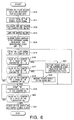
- timeslots used in the embodiment of the digital cellular phone operable as a communication device are described with reference to Fig. 6.
- the communication device is assumed to be used in a digital cellular system (PDS) in JAPAN.
- the system employs three-slots TDMA.
- This method uses a plurality of super frames each of which is sequentially continued and which is divided into 36 groups (from the first group to the 36-th group) and each group corresponds to a unique number identifying a cellular phone.
- description has been restricted to the three-slots TDMA. However, it is possible to apply the method and the device according to this invention to the other communication methods when they employ an intermittent receiving method which ensures that the communication device receives/sends a signal at a fixed or a regular interval.
- status transitions of the power supply of the radio unit 102, the reference oscillator 108, and the demodulation clock unit 125 are illustrated together with status transitions of operations of the counter 151 and the counter 153, and status transition of the switch 145.
- data receiving time intervals A and B are represented, each of which lasts for 6.7 ms.
- a time period between the starting points of the receiving periods A and B is equal to 720 ms.
- the controller 109 illustrated in Fig. 1 supplies, at a step S10 (Fig. 7), power to the radio unit 102, the reference oscillator 108, the demodulating clock unit 125 (Fig. 2) of the demodulating unit 103, and the other circuit blocks necessary for receiving data.
- the step S10 proceeds to a step S11 at which data reception is started by the digital cellular phone.
- the clock reproducing unit 124 (Fig. 2) in the demodulating unit 103 adjusts timing of the symbol clock signal 136 so as to match symbol timing of the received signal with that of the symbol clock signal 136.
- the step S11 in Fig. 7 is followed by a step S12 at which the controller 109 (Fig. 1) calculates a value supplied to the counter 152 (Fig. 4) and a value supplied to the counter 153 (Fig. 4), and sets the values to the corresponding counters.
- the value supplied to the counter 152 serves to stop counting the clock signal 134
- the value supplied to the counter 153 serves to stop counting the modulation clock signal 133.
- the counters 152 and 153 serve as the time measuring unit to measure elapse of a predetermined period.
- the frequency (32.768kHz) of the clock signal 134 which is generated by the oscillator 161 (Fig.
- the controller 19 sends the controller signal 135 to the time measuring unit 126 (Fig. 2) of the demodulating unit 103. Responsive to the controller signal 135, the time measuring unit 126 (Fig. 4) supplies the control signal 132 to the clock reproducing unit 124 (Fig. 3). Supplied with the control signal 132, the clock reproducing unit 124 controls the switch 145 and stops the power supply by the switch 145.
- a time period for which the clock reproducing unit 124 is to be stopped is equal to 710 ms.
- the time period is determined, for example, by subtracting an allowance time from a time interval (713.3 ms) for which a communication device is not needed to receive data in the three-slots TDMA used in a digital cellular phone system (PDC) which will be explained later in connection to Fig. 6.
- a time interval 713.3 ms
- PDC digital cellular phone system
- the process at the step S13 (Fig. 7) shuts off the power supply by the switch 145.
- This timing corresponds to the first trailing edge of the waveform shown in Fig. 8 for the switch 145.
- the processes at steps S10 to S12 are done before the first trailing edge, and the first data receiving time interval A also ends at the first trailing edge.
- the value of the counter 143 is a positive integer and generally takes either one value from one to 128 cyclically.
- the above cycle from one to 128 corresponds to a cycle of the symbol clock signal. Since the value represents the phase timing of the symbol clock when the switch 145 is powered off and the value is held for the period which the switch 145 is powered off, the symbol clock can be restarted without causing phase shift to occur.
- the controller 109 suspends the power supply of the radio unit 102, the reference oscillator 108, and the demodulating clock unit 125.
- the above suspending processes are gathered into the step S14, process related to the radio unit 102 and the other processes should be performed at different timing from each other in the strict sense.
- the suspending process of the radio unit 102 is performed simultaneously with the power off of the switch 145, that is, the radio unit 102 may temporarily be put in an inactive state after data reception.
- the power supplies of the reference oscillator 108 and the demodulation clock unit 125 may be suspended after the suspending process of the radio unit 102 (such suspension may be carried out after a step S15).
- the reference frequency signal of the reference oscillator 108 is used to sort data or to decrypt the data signal after reception the data signal while the clock signal of the demodulation clock unit 125 is used to control timing of the other devices after reception of the data signal.
- the process in the step S14 corresponds to each of the first trailing edges of the waveforms shown in Fig. 8 of the radio unit 102, the reference oscillator 108, and the demodulation clock unit 125.
- power supplies to the reference oscillator 108 and the demodulation clock unit 125 are suspended a moment after the power supply of the radio unit 125 is suspended.
- the controller 109 start to count up the clock signal 134 using the counter 151.
- the processes at the steps S13 to S15 are sequentially performed for convenience of the description. However, the processes, in fact, may be performed almost simultaneously.
- the counter 151 is activated. This operation corresponds to the first leading edge of the waveform of the counter 151, as shown in Fig. 8, and counting the clock signal 134 is started from this time point.
- the value ⁇ is representative of a spare time or the allowance time which is previously prepared to activate the reference oscillator 108 or the demodulating clock unit 125 so that the counter 153 can be quickly put into an active state immediately when the value of the counter 151 becomes equal to the value ⁇ .
- the allowance time is representative of a time interval from a start of power supply to a stable state of each of the reference oscillator 108 or the demodulating clock unit 125.
- the time interval may be equal to 3 milliseconds or so.
- the value ⁇ is representative of an allowance time which is prepared to activate the radio unit 102 in advance so that received data signal can be immediately demodulated when the value of the counter 151 becomes equal to the value ⁇ . Since it is necessary that the radio unit 102 is activated in advance at a step S20 so that the unit 102 operates normally when the value of the counter 153 becomes equal to the value in the comparator 154, the determination should be originally performed in the second loop shown in Fig.
- a time interval counted by using the counter 153 is about 2.6 ⁇ s and therefore is very short.
- a period time from a start of power supply to the radio unit 102 to a stable operation of the radio unit 102 is about 100 ⁇ s. Therefore, in this embodiment, the time point to restart supplying power of the radio unit 102 should be determined in the first loop shown in Fig. 7 (the loop including steps S15 to S18).
- step S17 if the value of the counter 151 is not equal to the value ⁇ , the process proceeds to a step S18 at which it is determined whether or not the value of the counter 151 is equal to the value in the comparator 152.
- step S18 if it is determined that the value of the counter 151 is not equal to the value in the comparator 152, the process returns to step S15 and then, counting the clock signal 134 is repeated.
- step S18 the process proceeds to step S19 at which the counter 153 is activated to count the demodulation clock signal 133.
- a time point at which the counter 153 starts counting at the step S19 can be made to correspond to the second leading edge of the waveform of the counter 153, as shown in Fig. 8.
- the counter 151 is stopped, as depicted by 151 in Fig. 8.
- the reference oscillator 108, the demodulation clock unit 125, and the radio unit 102 are supplied with power before the counter 151 is put into the inactive state, as readily understood from the steps S22 and S23 described later.
- step S20 the process proceeds to a step S20 at which it is determined that the value of the counter 153 is equal to the value in the comparator 154.
- step S19 If the result of the determination is false (NO), the process returns to step S19 and counting the demodulation clock signal 133 is repeated. If the result of the determination is true (YES), the process proceeds to a step S21, power is supplied to the switch 145, and counting the demodulation clock signal 133 is restarted by the counter 143. As described above, since the counter 143 remains holding the phase value when the power supply of the switch 145 is suspended, that is, the value before 710 ms, counting is performed from the value and therefore, it is possible to generate the symbol clock signal 136 without any phase shift.
- a time point at which demodulating the received data is prepared at step S21 corresponds to the second leading edge of the waveform depicted by 153 in Fig. 8. Also, it is found that the switch 145 is turned on at this time point.
- a suspending time lasts for 710 ms from the end of the data receiving period A until the data signal can be received.
- the allowance time is set in consideration of unevenness among starting operation times of elements in the communication device or the like. But, if the unevenness problem is resolved, the allowance time may be closer to zero. In this case, the suspending time should be still a multiple of a frequency of the symbol timing (21 kHz).
- step S12 in Fig. 7 that is, a procedure to determine values to be set to the comparators 152 and 154 in the time measuring unit 126.
- deviation of the clock signal 134 is calculated.
- the principle of derivation of the correcting value 164 of the clock unit 105 (principle of clock correcting circuit) the following equation is determined.
- deviation X (ppm) -1 * (H - 1,209,375) * (100 / 120)
- a frequency F1 of the clock signal 134 can be represented by the equation.
- F1 32.768 * (1 + X / 1,000,000) (kHz)
- a count value of the clock signal 134 is n1d, that is 710 ms /(1/F1)).
- H 1,209,365
- calculations are made as the following equations.
- n2 38.
- T1 and T2 are determined from the above calculation.
- a value of T1 plus T2 is not always equal to a value of T, since T is represented using two kinds of frequencies of clock signals (T1, T2).
- the communication device of the invention it is possible to suspend power supply to the radio unit 102, the reference oscillator 108, and the demodulating unit 103 at all the time period except during the device is expected to receive a call signal.
- the device according to the invention can reduce power consumption by using only the lowest frequency of clock signal during the suspending time period.
- the device according to the invention prepares a plurality of counters not to cause a phase shift of the symbol clock signal in restarting the power supply, and thereby can regenerate proper symbol clock signal.
- the device according to the invention can precisely measure a time period relating to intermittent radio signal receiving by using a lower frequency of clock signal and a higher frequency of clock signal, and thereby can reduce power consumption.
Landscapes
- Engineering & Computer Science (AREA)
- Computer Networks & Wireless Communication (AREA)
- Signal Processing (AREA)
- Synchronisation In Digital Transmission Systems (AREA)
- Mobile Radio Communication Systems (AREA)
- Telephone Function (AREA)
- Digital Transmission Methods That Use Modulated Carrier Waves (AREA)
- Electric Clocks (AREA)
- Circuits Of Receivers In General (AREA)
Applications Claiming Priority (2)
| Application Number | Priority Date | Filing Date | Title |
|---|---|---|---|
| JP2716399 | 1999-02-04 | ||
| JP02716399A JP3560489B2 (ja) | 1999-02-04 | 1999-02-04 | 効率的に電源供給を制御する通信装置、制御方法、及び記録媒体 |
Publications (2)
| Publication Number | Publication Date |
|---|---|
| EP1026829A2 true EP1026829A2 (fr) | 2000-08-09 |
| EP1026829A3 EP1026829A3 (fr) | 2003-12-03 |
Family
ID=12213401
Family Applications (1)
| Application Number | Title | Priority Date | Filing Date |
|---|---|---|---|
| EP00102110A Withdrawn EP1026829A3 (fr) | 1999-02-04 | 2000-02-04 | Procedé et Circuit de commuter l'alimentation dans un appareil de communications |
Country Status (4)
| Country | Link |
|---|---|
| US (1) | US6615060B1 (fr) |
| EP (1) | EP1026829A3 (fr) |
| JP (1) | JP3560489B2 (fr) |
| CN (1) | CN1130091C (fr) |
Cited By (3)
| Publication number | Priority date | Publication date | Assignee | Title |
|---|---|---|---|---|
| GB2387508A (en) * | 2002-04-12 | 2003-10-15 | Nec Technologies | Time base alignment in dual mode mobile telephone systems which calibrates a first and second master clock to a third clock |
| CN101729089B (zh) * | 2008-10-23 | 2013-07-10 | 弥亚微电子(上海)有限公司 | 通信系统的发射机、接收机及其同步方法 |
| CN103490796A (zh) * | 2013-09-13 | 2014-01-01 | 北京师范大学 | 一种配电线宽带电力载波通信系统及方法 |
Families Citing this family (16)
| Publication number | Priority date | Publication date | Assignee | Title |
|---|---|---|---|---|
| JP3389140B2 (ja) | 1999-04-20 | 2003-03-24 | エヌイーシーアクセステクニカ株式会社 | 間欠受信装置 |
| US6947721B2 (en) * | 2000-05-15 | 2005-09-20 | Texas Instruments Incorporated | Wireless communications with transceiver-integrated frequency shift control and power control |
| JP2002051004A (ja) * | 2000-05-24 | 2002-02-15 | Seiko Instruments Inc | 電力供給装置及び携帯情報機器 |
| KR100799138B1 (ko) * | 2001-03-12 | 2008-01-29 | 스카이워크스 솔루션즈 인코포레이티드 | 광대역 코드 분할 다중 접속 시스템의 다경로 신호를검출, 식별 및 모니터링하는 방법 및 기기 |
| JP3636097B2 (ja) * | 2001-06-05 | 2005-04-06 | 三菱電機株式会社 | 無線通信装置及びその受信タイミング推定方法 |
| US7292832B2 (en) * | 2001-09-17 | 2007-11-06 | Analog Device, Inc. | Timing and frequency control method and circuit for digital wireless telephone system terminals |
| JP2003110484A (ja) * | 2001-09-27 | 2003-04-11 | Sony Corp | 携帯通信端末、該携帯通信端末における通信方法、プログラムおよび該プログラムを記録した記録媒体 |
| KR100764989B1 (ko) * | 2001-10-29 | 2007-10-09 | 엘지노텔 주식회사 | 파워드-허브에서 파워 공급 장치 및 방법 |
| JP4064150B2 (ja) * | 2002-05-20 | 2008-03-19 | シャープ株式会社 | 無線通信装置及び無線通信装置の制御方法 |
| US7477713B2 (en) * | 2004-03-02 | 2009-01-13 | International Business Machines Corporation | method for providing automatic adaptation to frequency offsets in high speed serial links |
| US20050221870A1 (en) * | 2004-04-06 | 2005-10-06 | Integration Associates Inc. | Method and circuit for determining a slow clock calibration factor |
| US8462858B2 (en) * | 2005-02-18 | 2013-06-11 | Texas Instruments Incorporated | Wireless communications with transceiver-integrated frequency shift control and power control |
| JP2008124524A (ja) * | 2005-03-04 | 2008-05-29 | Matsushita Electric Ind Co Ltd | 間欠受信制御装置 |
| WO2006123493A1 (fr) * | 2005-05-20 | 2006-11-23 | Matsushita Electric Industrial Co., Ltd. | Appareil de terminal de communication |
| KR100853189B1 (ko) * | 2006-12-08 | 2008-08-20 | 한국전자통신연구원 | 태그 수명 연장을 위한 저전력 무선 인식 태그 및 그 방법 |
| US9182780B2 (en) * | 2012-05-16 | 2015-11-10 | Broadcom Corporation | Power management unit including a signal protection circuit |
Family Cites Families (8)
| Publication number | Priority date | Publication date | Assignee | Title |
|---|---|---|---|---|
| US5428820A (en) | 1993-10-01 | 1995-06-27 | Motorola | Adaptive radio receiver controller method and apparatus |
| US5613235A (en) * | 1995-06-29 | 1997-03-18 | Nokia Mobile Phones Limited | Operation of a radiotelephone in a synchronous extended standby mode for conserving battery power |
| JP3555252B2 (ja) * | 1995-06-30 | 2004-08-18 | 株式会社デンソー | 間欠受信制御装置 |
| US5943613A (en) * | 1996-11-07 | 1999-08-24 | Telefonaktiebolaget Lm Ericsson | Method and apparatus for reducing standby current in communications equipment |
| JPH10190568A (ja) * | 1996-12-27 | 1998-07-21 | Matsushita Electric Ind Co Ltd | 無線受信装置 |
| US6029061A (en) * | 1997-03-11 | 2000-02-22 | Lucent Technologies Inc. | Power saving scheme for a digital wireless communications terminal |
| US6081733A (en) * | 1997-04-16 | 2000-06-27 | Motorola, Inc. | Communication control apparatus and method |
| US6088602A (en) * | 1998-03-27 | 2000-07-11 | Lsi Logic Corporation | High resolution frequency calibrator for sleep mode clock in wireless communications mobile station |
-
1999
- 1999-02-04 JP JP02716399A patent/JP3560489B2/ja not_active Expired - Fee Related
-
2000
- 2000-02-02 US US09/496,541 patent/US6615060B1/en not_active Expired - Lifetime
- 2000-02-03 CN CN00104695A patent/CN1130091C/zh not_active Expired - Fee Related
- 2000-02-04 EP EP00102110A patent/EP1026829A3/fr not_active Withdrawn
Cited By (5)
| Publication number | Priority date | Publication date | Assignee | Title |
|---|---|---|---|---|
| GB2387508A (en) * | 2002-04-12 | 2003-10-15 | Nec Technologies | Time base alignment in dual mode mobile telephone systems which calibrates a first and second master clock to a third clock |
| GB2387508B (en) * | 2002-04-12 | 2005-06-29 | Nec Technologies | Mobile radio communications device and method of operation |
| CN101729089B (zh) * | 2008-10-23 | 2013-07-10 | 弥亚微电子(上海)有限公司 | 通信系统的发射机、接收机及其同步方法 |
| CN103490796A (zh) * | 2013-09-13 | 2014-01-01 | 北京师范大学 | 一种配电线宽带电力载波通信系统及方法 |
| CN103490796B (zh) * | 2013-09-13 | 2015-04-15 | 北京师范大学 | 一种配电线宽带电力载波通信系统及方法 |
Also Published As
| Publication number | Publication date |
|---|---|
| EP1026829A3 (fr) | 2003-12-03 |
| US6615060B1 (en) | 2003-09-02 |
| CN1130091C (zh) | 2003-12-03 |
| JP2000224100A (ja) | 2000-08-11 |
| CN1265556A (zh) | 2000-09-06 |
| JP3560489B2 (ja) | 2004-09-02 |
Similar Documents
| Publication | Publication Date | Title |
|---|---|---|
| US6615060B1 (en) | Communication device effectively controlling power supply, method of controlling power supply, and medium | |
| CA2220258C (fr) | Partie receptrice d'un dispositif de communication radio | |
| JP3193380B2 (ja) | モービル通信受信機における電力消費を減少する装置および方法 | |
| JP3689021B2 (ja) | タイミング制御装置及びタイミング制御方法 | |
| US5457716A (en) | Automatic frequency control in a radio communication receiver | |
| US6542727B1 (en) | Receiving control apparatus and method thereof | |
| EP0622966B1 (fr) | Récepteur d'appel de personnes par radio avec une précision améliorée de la sychronisation de trame | |
| JP3272273B2 (ja) | 間欠受信装置 | |
| EP1395072B1 (fr) | Appareil de communication radio et procede d'estimation de temps de reception associe | |
| US6049708A (en) | Mobile communication apparatus for intermittently receiving a broadcasting signal at a corrected reception timing | |
| JP4001686B2 (ja) | 受信機及び間欠フレーム同期方法及び携帯端末 | |
| JP3288196B2 (ja) | 移動体通信端末 | |
| JP2003078427A (ja) | 携帯電話端末及びそれに用いる間欠受信制御方法並びにそのプログラム | |
| JP3439448B2 (ja) | 効率的に電源供給を制御する通信装置、制御方法、及び記録媒体 | |
| JP2897684B2 (ja) | 無線送受信装置 | |
| JP3389140B2 (ja) | 間欠受信装置 | |
| GB2368235A (en) | Preventing data losses due to timing errors in a receiver operating in a power-saving mode | |
| JPH09321687A (ja) | 無線通信機器 | |
| JP2002368729A (ja) | 無線通信端末 | |
| JP2008005336A (ja) | 受信装置、受信処理方法、及びベースバンドプロセッサ | |
| JP2001069107A (ja) | 受信制御装置 | |
| JP2000049682A (ja) | 携帯電話端末 | |
| JP2001060865A (ja) | クロック生成回路および周波数補正方法 | |
| JP3876405B2 (ja) | 移動機及び間欠受信制御方法 | |
| JPH0993185A (ja) | 間欠受信装置 |
Legal Events
| Date | Code | Title | Description |
|---|---|---|---|
| PUAI | Public reference made under article 153(3) epc to a published international application that has entered the european phase |
Free format text: ORIGINAL CODE: 0009012 |
|
| AK | Designated contracting states |
Kind code of ref document: A2 Designated state(s): AT BE CH CY DE DK ES FI FR GB GR IE IT LI LU MC NL PT SE |
|
| AX | Request for extension of the european patent |
Free format text: AL;LT;LV;MK;RO;SI |
|
| PUAL | Search report despatched |
Free format text: ORIGINAL CODE: 0009013 |
|
| AK | Designated contracting states |
Kind code of ref document: A3 Designated state(s): AT BE CH CY DE DK ES FI FR GB GR IE IT LI LU MC NL PT SE |
|
| AX | Request for extension of the european patent |
Extension state: AL LT LV MK RO SI |
|
| 17P | Request for examination filed |
Effective date: 20031022 |
|
| AKX | Designation fees paid |
Designated state(s): DE FR GB IT |
|
| 17Q | First examination report despatched |
Effective date: 20050714 |
|
| STAA | Information on the status of an ep patent application or granted ep patent |
Free format text: STATUS: THE APPLICATION IS DEEMED TO BE WITHDRAWN |
|
| 18D | Application deemed to be withdrawn |
Effective date: 20090606 |