EP1027642B1 - Microprocesseur comprenant des moyens de concatenation de bits - Google Patents
Microprocesseur comprenant des moyens de concatenation de bits Download PDFInfo
- Publication number
- EP1027642B1 EP1027642B1 EP98950180A EP98950180A EP1027642B1 EP 1027642 B1 EP1027642 B1 EP 1027642B1 EP 98950180 A EP98950180 A EP 98950180A EP 98950180 A EP98950180 A EP 98950180A EP 1027642 B1 EP1027642 B1 EP 1027642B1
- Authority
- EP
- European Patent Office
- Prior art keywords
- concatenation
- bit
- regbank
- instruction
- microprocessor
- Prior art date
- Legal status (The legal status is an assumption and is not a legal conclusion. Google has not performed a legal analysis and makes no representation as to the accuracy of the status listed.)
- Expired - Lifetime
Links
Images
Classifications
-
- G—PHYSICS
- G06—COMPUTING OR CALCULATING; COUNTING
- G06F—ELECTRIC DIGITAL DATA PROCESSING
- G06F9/00—Arrangements for program control, e.g. control units
- G06F9/06—Arrangements for program control, e.g. control units using stored programs, i.e. using an internal store of processing equipment to receive or retain programs
- G06F9/30—Arrangements for executing machine instructions, e.g. instruction decode
- G06F9/30003—Arrangements for executing specific machine instructions
- G06F9/30007—Arrangements for executing specific machine instructions to perform operations on data operands
- G06F9/30018—Bit or string instructions
-
- G—PHYSICS
- G06—COMPUTING OR CALCULATING; COUNTING
- G06F—ELECTRIC DIGITAL DATA PROCESSING
- G06F9/00—Arrangements for program control, e.g. control units
- G06F9/06—Arrangements for program control, e.g. control units using stored programs, i.e. using an internal store of processing equipment to receive or retain programs
- G06F9/30—Arrangements for executing machine instructions, e.g. instruction decode
- G06F9/30003—Arrangements for executing specific machine instructions
- G06F9/30007—Arrangements for executing specific machine instructions to perform operations on data operands
- G06F9/30032—Movement instructions, e.g. MOVE, SHIFT, ROTATE, SHUFFLE
Definitions
- the present invention relates to microprocessors, and more particularly the production in a microprocessor of a concatenation operation at least one bit of a first binary word with bits of a second binary word.
- Bit concatenation is an operation frequently used in industrial computing.
- the authentication codes issued by microprocessor cards like bank cards are generated by cryptographic algorithms requiring many bit concatenation operations.
- Gold conventional microprocessors have the disadvantage to consume several clock cycles and several bytes of program code to perform this operation.
- bit concatenation is done using the "BRSET” and "BCLR" instructions and requires first setting the bits of a memory zone intended for 1 contain the result of the operation. Then we test the value of a first bit to be concatenated and we set the first bit of the memory area if the bit to be concatenated is equal to 0. Then, we test the value of a second bit at concatenate and set the second bit of the zone to 0 memory if the second bit to concatenate is equal to 0, etc.
- the concatenation of each bit in the memory area requires five bytes of program code (instructions and memory addressing) and execution time is about ten machine cycles.
- a microprocessor of the type 8051 one charges first of all the bit to concatenate in a flag ("flag"), for example the CRY flag ("Carry"). Then, we insert the bit in the working register of the microprocessor, by right shift from register to by means of the "MMR” instruction or by direct insertion into by means of the "MOV” instruction. Finally, the content of work register is loaded into memory. These operations also consume multiple bytes of code and several machine cycles.
- microprocessors pipeline-type systems i.e. overlapping instructions, the advantage of which is operate at high speed.
- these microprocessors are complex, bulky and a cost that makes them unfit to be integrated into smart cards.
- contactless smart cards powered by electromagnetic induction have low electrical energy resources and must be equipped with a microprocessor which consumes little current while being fast and able to process a transaction in a very short time, on the order of a few milliseconds.
- EP-A-0 664 508 describes a processor particularly suitable for bit transfer.
- US patent 4,023,023 describes a circuit hardware allowing various operations to be carried out bit shift and concatenation from two binary words provided as input.
- a general objective of the present invention is to provide a microprocessor which incorporates a circuit bit concatenation hardware while being simple design, small footprint and small consumption, and which offers a high speed of processing program instructions, including a concatenation instruction.
- a pipeline microprocessor comprising means for decoding of a concatenation instruction of at least one bit of a first binary word with at least one bit of a second binary word; a register bank; of means for processing the concatenation instruction; a first stage pipeline comprising the means of decoding the concatenation instruction; a second pipeline stage, contiguous to the first stage, comprising a first sector comprising concatenation means, in which the register bank is arranged in reading, and a second sector in which the bank of registers is arranged in writing, the first sector being active at each clock half cycle of the microprocessor and the second active sector at each next half clock cycle, the processing means the concatenation instruction being arranged to read the first and second binary words in the bank of registers and execute the concatenation instruction at during a first half clock cycle, and record the result of the concatenation in the bank of registers during the next clock half cycle.
- the means of concatenation include means of presentation in parallel, on the microprocessor data path, of the two words binaries read from the registry bank, means of selection of at least one bit to concatenate the first word binary, and means for shifting bits from the second binary word on the data path and insert it into the second binary word at least the selected bit of the first binary word.
- the means for shifting bits include a hardware-switched wire circuit arranged for, on reception of an offset signal, shift the row of wires in the data path and connect to at least one wire of the data path the output of the means for selecting the bit to be concatenated.
- the means of selection of at least one bit include a circuit multiplexer arranged on the data path for receive the first binary word as input.
- the second word binary is read in the register bank at the address recording the result of the concatenation.
- the microprocessor includes means for decoding an instruction concatenation compact with a compact address recording the result of the concatenation.
- the microprocessor includes means for decoding an instruction of concatenation whose code includes a compact address predetermined recording of the result of the concatenation.
- the means of decoding of the concatenation instruction are arranged to generate a fixed and predetermined address recording the result of the concatenation.
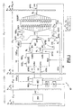
- FIG. 1 represents a microprocessor MP according to the invention, operating here under 16 bits and of the pipeline type, that is to say with instruction overlap.
- the microprocessor is organized to execute compact instructions in the following format: OP CODE ADRd ADRs -
- These instructions include a code OP code of the operation to be executed, coded on 4 bits, the address ADRd of a register Rd of destination of the result, on 4 bits, and the address ADRs d 'a source register Rs, on 4 bits (here, the last field of the instruction is not used).
- the operation is for example the addition ADD (add Rs and Rd and store the result in Rd), the subtraction SUB (subtract Rs from Rd and store the result in Rd), the logical OR (store in Rd the result of Rs OR Rd), the logical AND, etc.
- the microprocessor is also organized to execute a compact instruction of BMV concatenation, according to the following format: CODE BMV ADRd ADRs ADbi
- This instruction includes the code CODE BMV of the concatenation operation, on 4 bits, the address ADRd of the register Rd of destination of the result of the concatenation, on 4 bits, the address ADRs of a source register Rs, on 4 bits, and the address (or rank) ADb 1 of a bit b 1 of the source register Rs.
- the general structure of the microprocessor according to the invention will first be described, which comprises a program memory MEM, a bank of registers REGBANK, an arithmetic and logic calculation unit ALU, an ordinal counter PC, an SPC circuit for incrementing the PC ordinal counter and a DEC1 instruction decoder.
- the microprocessor also comprises concatenation means taking the form of a BSHIFT shift circuit and a MUX circuit for selecting, as a function of the address ADb i , the bit b i to be concatenated.
- the DEC1 decoder, the ALU unit and the REGBANK bank are circuits or circuit sets well known to those skilled in the art and their internal structure will not be described.
- the decoder DEC1 is connected to the memory output MEM for receive instructions from a program to be executed.
- the ALU unit here has two inputs IN1, IN2, one OUT output, and is controlled by a DEC2 decoder.
- the REGBANK register bank contains various registers of work, for example sixteen registers R0 to R15 (no represented).
- REGBANK bank has an IADRs entry for the address ADRs of the source register Rs, an entry IADRd for the address of the destination register Rd, a output OUTRs for reading the source register Rs, one output OUTRd for reading the destination register Rd, and a INRd input for writing a result to the destination register Rd.
- the bank's output OUTRd REGBANK is connected to input IN1 of the ALU unit.
- the OUTRs output is connected to the IN2 input of the ALU unit and at the entrance of the MUX circuit.
- the BSHIFT circuit includes sixteen bit inputs e 0 to e 15 connected to the OUT output of the ALU, an auxiliary input e 16 connected to the output of the MUX circuit, and sixteen bit outputs s 0 to s 15 forming the termination of the DPTH data path of the microprocessor, these outputs being connected to the INRd input of the REGBANK bank.
- the DPTH data path of the microprocessor first includes two tracks of sixteen threads at the exit from REGBANK bank, then a sixteen-wire lane and an auxiliary wire at the input of the BSHIFT circuit, and finally a channel of sixteen wires from the circuit output BSHIFT up to the entrance to REGBANK bank.
- connections from the termination of the path DPTH data are of course conceivable, for example a connection to the MEM memory or to another memory of data storage.
- the BSHIFT circuit is controlled by an SR signal. When this signal is at 0, the BSHIFT circuit is transparent and the outputs s 15 to s 0 copy the inputs e 15 to e 0 . When the BSHIFT signal is at 1, the circuit shifts its outputs relative to its inputs. The outputs s 14 to s 0 copy the inputs e 15 to e 1 , respectively, and the output s 15 copies the auxiliary input e 16 . In this case, the entry e 0 is disconnected from the data path.
- the microprocessor is by elsewhere organized in two stages pipeline ST1, ST2 contiguous, delimited by locking registers B1, B3 (or "latch"). These registers B1, B3 are unlocked by the rising edge of a clock signal H1.
- Memory MEM and decoder DEC1 are arranged in the first ST1 floor.
- REGBANK bank, ALU unit, MUX multiplexer and the BSHIFT circuit are arranged in the second stage ST2.
- the two stages ST1, ST2 are each divided into two sectors ST11 / ST12, respectively ST21 / ST22.
- the sectors ST11 / ST12 are delimited by a register B2 arranged between the output of the memory MEM and the decoder DEC1.
- the sectors ST21 / ST22 are delimited by a register B4 arranged between the outputs s 0 to s 15 of the BSHIFT circuit and the input INRd of the REGBANK bank.
- the register B2 is a locking register unlocked by the rising edge of a signal H2 180 ° phase shifted relative to the signal H1.
- the register B4 is preferably a three-state buffer ("buffer tristate") transparent when the signal H2 is at 1, and in the high impedance state when the signal H2 is at 0.
- the clock signal H1 synchronizes the transfer of data from stage ST1 to stage ST2, and the signal H2 synchronizes the transfer of data from the first sector ST11, ST21 to the second sector ST12, ST22 of each pipeline stage.
- the clock signals H1 and transfer H2 are shown at the bottom of Figure 1.
- REGBANK bank is read controlled by a RDH1 signal and in writing by a WRH2 signal. These signals are sent by the decoder DEC1.
- the signal from read RDH1 is emitted when the clock signal H1 passes at 1 and the write signal WRH2 is emitted when the signal H2 goes to 1.
- the REGBANK bank thus belongs, in reading, to the first sector ST21 of the stage ST2 and, in write, to the second sector ST22 of the stage ST2.
- the memory MEM delivers the instruction contained at the address provided by the PC ordinal counter on reception of the read signal RDH1.
- steps 3.1 and 3.2 are steps to read and decode a new instruction (any) following the BMV instruction.
- steps 2.3 and 2.4 are carried out in a single clock cycle. Furthermore, due to the microprocessor pipeline operation, the steps of reading 2.1 and decoding 2.2 overlap steps 1.3 and 1.4 of the previous instruction and do not consume the clock times.
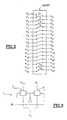
- FIG. 2 represents an advantageous embodiment of the BSHIFT circuit, by means of sixteen switches I0 to I15 controlled by the signal SR.
- Each switch I i is arranged to connect an output S i of rank i to an input e i of the same rank or to an input e i + 1 of higher rank, depending on the value of the signal SR.
- the switches I i can be produced by means of two CMOS switches T i and T i + 1 arranged between the output s i and the inputs e i and e i + 1 .
- the signal SR is applied to the NMOS transistor of the switch T i + 1 and to the PMOS transistor of the switch T i .
- An inverse signal / SR delivered by an inverting gate, is applied to the PMOS transistor of the switch T i + 1 and to the NMOS transistor of the switch T i .
- This bit shift by hardware wire switching BSHIFT circuit has the advantage, compared to a conventional shift register, of being able to receive the shift signal SR at the start of the clock cycle H1 before the data is stabilized on the inputs e 16 to e 0 .
- the provision of a conventional shift register remains possible, however, provided that a delay circuit is provided for the application of the signal SR.
- the bits concatenated in the register R0 are in bold characters.
- the bits in italics are the bits of low weight lost by right shift. In total, the concatenating the four bits requires only four pipeline clock cycles and a program of four instructions only.
- the address ADRd of the register Rd is automatically generated by the decoder DEC1 on reception of the code CODE BMV .
- the address ADRd can also be included in the CODE CODE BMV which can then be coded on 8 bits instead of 4.
- the least significant bit present on the input e 0 of the BSHIFT circuit can be preserved by means of a register LTCH as flag CRY ("Carry") of the microprocessor.
- the output of the register LTCH contains the flag CRY and is connected to the input e 16 of the circuit BSHIFT via a buffer BUF1, for the possible injection of the flag CRY in the data path.
- a second buffer BUF2 is interposed between the output of the circuit MUX and the input e16, to avoid collisions between the selected bit b i and the flag CRY.
- the decoder DEC1 controls the buffers BUF1 and BUF2 according to the type of instruction received.
- the decoder DEC1 sends the write signal WRH2 to the register LTCH for updating the flag CRY at the time of activation of the sector ST22, when a shift to the right has been made in the sector ST 21 during the half - previous clock cycle.
- the BSHIFT circuit can be used to perform arithmetic operations like the division or multiplication, which so require classic bit offsets. Otherwise, the BSHIFT circuit may be located at other points on the way data, for example between the bank output OUTRd REGBANK and input IN1 of the ALU unit.
- the concatenation of the bit b i can also be done by inserting the bit b i as a low weight on the input e 0 of the BSHIFT circuit and rotating the bits of the binary word W2 to the left.
- bit b i can be extended in a simple way to the simultaneous concatenation of several bits of the source register Rs, selected simultaneously by the circuit MUX.
- the provision of several cascaded BSHIFT circuits can make it possible to choose between the concatenation of a single bit, two bits at a time, three bits, etc.
- the choice of the number of bits to be concatenated can be coded in the CODE BMV field of the instruction.
- the compact addresses contained in the instructions can also be used to address the microprocessor memory plan.
- these addresses must be transformed into real addresses of the memory map by an address converter, called MMU ("Memory Management Unit).
- the microprocessor according to the invention is of a structure particularly simple ensuring low current consumption.
- An additional measure for limiting electricity consumption consists of having on the outputs OUTRs and OUTRd of the REGBANK bank of buffer circuits controlled by a signal H1 'shifted by duration ⁇ t relative to the signal H1.
- the ALU unit is not connected to the outputs OUTRs, OUTRd that when they are stabilized.
- the signal offset H1 ' can be obtained simply by means of a delay circuit, for example reversing doors in cascade.
- half clock cycle should not be interpreted restrictively. Indeed, at the speed of constant operation, it is equivalent to provide a clock signal having double speed and not activating the pipeline sectors that one clock cycle out of two, in shifting by one clock cycle the activation of each sector relative to the next sector.
- selecting a bit clock out of two as a control signal can be made in a simple way by means of a divider circuit of frequency, for example a rocker D whose output / Q is returned to input D.
- the control signals of the pipeline registers can also be combined in doors OR Exclusive before being applied, so to guarantee that two complementary sectors of the same pipeline floor will not be activated simultaneously.
Landscapes
- Engineering & Computer Science (AREA)
- Software Systems (AREA)
- Theoretical Computer Science (AREA)
- Physics & Mathematics (AREA)
- General Engineering & Computer Science (AREA)
- General Physics & Mathematics (AREA)
- Executing Machine-Instructions (AREA)
Description
- la figure 1 représente sous forme de blocs les principaux éléments d'un microprocesseur selon l'invention,
- la figure 2 représente un circuit à décalage selon l'invention, représenté schématiquement en figure 1, et
- la figure 3 représente un élément interrupteur du circuit à décalage de la figure 2.
| CODEOP | ADRd | ADRs | - |
| CODEBMV | ADRd | ADRs | ADbi |
| CODESUB | ADR1 | ADR2 | - |
| CODEBMV | ADR0 | ADR1 | 12 |
- le décodeur DEC1 émet le signal de lecture RDH1 et l'instruction SUB R1, R2 est lue dans la mémoire MEM.
- le décodeur DEC1 décode l'instruction SUB R1, R2, met le signal SR à 0, envoie les adresses ADR1 et ADR2 vers la banque REGBANK et envoie le code opération CODESUB de la soustraction vers l'unité ALU,
- le circuit SPC incrémente le compteur ordinal PC.
- la banque REGBANK reçoit les adresses ADR1, ADR2, le décodeur DEC2 reçoit le code CODESUB et le décodeur DEC1 émet le signal de lecture RDH1,
- les registres R1 et R2 sont lus et leur contenu appliqué sur les entrées IN1, IN2 de l'unité ALU,
- l'unité ALU délivre le résultat de la soustraction [R1-R2].
- le décodeur DEC1 émet le signal d'écriture WRH2,
- le circuit BSHIFT étant transparent (SR=0), le résultat de la soustraction [R1-R2] se retrouve sur l'entrée INRd de la banque REGBANK,
- le résultat de la soustraction [R1-R2] est enregistré dans le registre R1.
- le décodeur DEC1 émet le signal de lecture RDH1 et l'instruction BMV R0,R1,12 est lue dans la mémoire MEM.
- le décodeur DEC1 décode l'instruction BMV R0,R1,12, met le signal SR à 1, envoie les adresses ADR1 et ADR2 vers la banque REGBANK, envoie l'adresse ADbi = 12 vers le multiplexeur MUX, et envoie le code opération CODEBMV de la concaténation vers l'unité ALU,
- le circuit SPC incrémente le compteur ordinal PC.
- la banque REGBANK reçoit les adresses ADR1, ADR2, le décodeur DEC2 reçoit le code CODEBMV, le circuit MUX reçoit l'adresse ADBi (ici 12), le circuit BSHIFT reçoit le signal SR à 1 et le décodeur DEC1 émet le signal de lecture RDH1,
- le mot binaire W1 contenu dans le registre R1 est appliqué sur l'entrée du multiplexeur MUX et le mot binaire W2 contenu dans le registre R0 est appliqué sur l'entrée IN1 de l'unité ALU,
- selon l'invention, l'unité ALU recopie sur sa sortie OUT le mot W2 présent sur son entrée IN1,
- le multiplexeur MUX sélectionne le bit b12 qui se retrouve sur l'entrée auxiliaire e16 du circuit BSHIFT,
- le circuit BSHIFT connecte les sorties s14 à s0 aux
entrées e15 à e1, connecte la sortie s15 à l'entrée
auxiliaire e16, et délivre un mot binaire W3 de la forme
suivante :
W3 = b12 c15 c14 c13 c12 c11 c10 c9 c8 c7 c6 c5 c4 c3 c2 c1,
dans lequel le bit de plus fort poids est le bit b12 sélectionné dans le mot W1. Les autres bits du mot W3 sont des bits c15 à c1 du mot W2, le bit de plus faible poids c0 ayant été supprimé par le décalage.
- le mot W3 est appliqué sur l'entrée INRd de la banque REGBANK,
- le décodeur DEC1 émet le signal d'écriture WRH2 et le mot W3 est enregistré dans le registre R0 de la banque REGBANK.
| Cycle pipeline | Cycle pipeline | Cycle pipeline | |||
| 1/2 cycle | 1/2 cycle | 1/2 cycle | 1/2 cycle | ½ cycle | 1/2 cycle |
| H1=1 | H2=1 | H1=1 | H2=1 | H1=1 | H2=1 |
| étape 1.1 | étape 1.2 | étape 1.3 | étape 1.4 | ||
| étape 2.1 | étape 2.2 | étape 2.3 | étape 2.4 | ||
| étape 3.1 | étape 3.2 |

| CODEBMV | ADRs | ADbi |
Claims (8)
- Microprocesseur (MP), comprenant des moyens de décodage (DEC1) d'une instruction (BMV) de concaténation d'au moins un bit (bi) d'un premier mot binaire (W1) avec au moins un bit d'un deuxième mot binaire (W2), une banque de registres (REGBANK) et des moyens (REGBANK, MUX, BSHIFT) de traitement de l'instruction de concaténation (BMV), caractérisé en ce qu'il comprend :un premier étage pipeline (ST1) comprenant les moyens de décodage (DEC1) de l'instruction de concaténation,un deuxième étage pipeline (ST2), contigu au premier étage, comprenantun premier secteur (ST21) comprenant des moyens (OUTRd, OUTRs, MUX, BSHIFT) de concaténation, dans lequel la banque de registres (REGBANK) est agencée en lecture, etun deuxième secteur (ST22) dans lequel la banque de registres (REGBANK) est agencée en écriture,le premier secteur étant actif à chaque demi-cycle d'horloge du microprocesseur et le deuxième secteur actif à chaque demi-cycle d'horloge suivant,les moyens de traitement de l'instruction de concaténation étant agencés pour :lire les premier (W1) et deuxième (W2) mots binaires dans la banque de registres (REGBANK) et exécuter l'instruction de concaténation au cours d'un premier demi-cycle d'horloge, etenregistrer le résultat (W3) de la concaténation dans la banque de registres (REGBNANK) au cours du demi-cycle d'horloge suivant.
- Microprocesseur selon la revendication 1, dans lequel les moyens (MUX, BSHIFT) de concaténation (BMV) comprennent :des moyens (OUTRd, OUTRs) de présentation en parallèle, sur le chemin de données (DPTH) du microprocesseur, des deux mots binaires (W1, W2) lus dans la banque de registres (REGBANK),des moyens (MUX) de sélection d'au moins un bit (bi) à concaténer du premier mot binaire (W1), etdes moyens (BSHIFT) pour décaler des bits du deuxième mot binaire (W2) sur le chemin de données (DPTH) et insérer dans le deuxième mot binaire (W2) au moins le bit sélectionné (bi) du premier mot binaire (W1).
- Microprocesseur selon la revendication 2, dans lequel lesdits moyens pour décaler des bits comprennent un circuit (BSHIFT) à commutation matérielle de fils agencé pour, sur réception d'un signal de décalage (SR), décaler le rang des fils du chemin de données (DPTH) et connecter à au moins un fil (s15) du chemin de données la sortie (e16) des moyens (MUX) de sélection du bit (bi) à concaténer.
- Microprocesseur selon l'une des revendications 2 et 3, dans lequel les moyens de sélection d'au moins un bit comprennent un circuit multiplexeur (MUX) agencé sur le chemin de données (DPTH) pour recevoir en entrée le premier mot binaire (W1).
- Microprocesseur selon l'une des revendications 1 à 4, dans lequel le deuxième mot binaire (W2) est lu dans la banque de registres (REGBANK) à l'adresse (ADRd) d'enregistrement du résultat (W3) de la concaténation.
- Microprocesseur selon l'une des revendications 1 à 5, comprenant des moyens de décodage (DEC1) d'une instruction compacte de concaténation (BMV) comportant une adresse compacte (ADRd) d'enregistrement du résultat (W3) de la concaténation.
- Microprocesseur selon l'une des revendications 1 à 5, comprenant des moyens de décodage (DEC1) d'une instruction de concaténation (BMV) dont le code (CODEBMV) comporte une adresse compacte (ADRd) prédéterminée d'enregistrement du résultat (W3) de la concaténation.
- Microprocesseur selon l'une des revendications 1 à 5, dans lequel les moyens de décodage (DEC1) de l'instruction de concaténation (BMV) sont agencés pour générer une adresse (ADRd) fixe et prédéterminée d'enregistrement du résultat (W3) de la concaténation.
Applications Claiming Priority (3)
| Application Number | Priority Date | Filing Date | Title |
|---|---|---|---|
| FR9713758 | 1997-11-03 | ||
| FR9713758A FR2770661B1 (fr) | 1997-11-03 | 1997-11-03 | Microprocesseur comprenant des moyens de concatenation de bits |
| PCT/FR1998/002266 WO1999023550A1 (fr) | 1997-11-03 | 1998-10-23 | Microprocesseur comprenant des moyens de concatenation de bits |
Publications (2)
| Publication Number | Publication Date |
|---|---|
| EP1027642A1 EP1027642A1 (fr) | 2000-08-16 |
| EP1027642B1 true EP1027642B1 (fr) | 2001-08-29 |
Family
ID=9512939
Family Applications (1)
| Application Number | Title | Priority Date | Filing Date |
|---|---|---|---|
| EP98950180A Expired - Lifetime EP1027642B1 (fr) | 1997-11-03 | 1998-10-23 | Microprocesseur comprenant des moyens de concatenation de bits |
Country Status (6)
| Country | Link |
|---|---|
| US (1) | US6317825B1 (fr) |
| EP (1) | EP1027642B1 (fr) |
| AU (1) | AU1550799A (fr) |
| DE (1) | DE69801513T2 (fr) |
| FR (1) | FR2770661B1 (fr) |
| WO (1) | WO1999023550A1 (fr) |
Families Citing this family (4)
| Publication number | Priority date | Publication date | Assignee | Title |
|---|---|---|---|---|
| FR2770661B1 (fr) * | 1997-11-03 | 2001-08-10 | Inside Technologies | Microprocesseur comprenant des moyens de concatenation de bits |
| EP1046125B1 (fr) * | 1998-09-30 | 2008-12-24 | Nxp B.V. | Support de donnees |
| JP6382880B2 (ja) * | 2016-04-13 | 2018-08-29 | 任天堂株式会社 | 振動制御システム、振動制御方法、振動出力装置、ゲームコントローラ、振動出力プログラム、および振動出力方法 |
| JP7433931B2 (ja) * | 2020-01-27 | 2024-02-20 | キヤノン株式会社 | 情報処理装置及びその制御方法及びプログラム |
Family Cites Families (6)
| Publication number | Priority date | Publication date | Assignee | Title |
|---|---|---|---|---|
| FR2253415A5 (fr) * | 1973-12-04 | 1975-06-27 | Cii | |
| US4785393A (en) * | 1984-07-09 | 1988-11-15 | Advanced Micro Devices, Inc. | 32-Bit extended function arithmetic-logic unit on a single chip |
| FR2655748B1 (fr) * | 1989-12-07 | 1992-01-24 | Bull Sa | Circuit decaleur avec generateur de bits de parite. |
| JPH03211613A (ja) * | 1990-01-17 | 1991-09-17 | Toshiba Corp | ディジタル信号処理装置 |
| JP2932963B2 (ja) * | 1994-01-21 | 1999-08-09 | モトローラ・インコーポレイテッド | 効率的なビット移動能力を有するデータ・プロセッサとその方法 |
| FR2770661B1 (fr) * | 1997-11-03 | 2001-08-10 | Inside Technologies | Microprocesseur comprenant des moyens de concatenation de bits |
-
1997
- 1997-11-03 FR FR9713758A patent/FR2770661B1/fr not_active Expired - Fee Related
-
1998
- 1998-10-23 WO PCT/FR1998/002266 patent/WO1999023550A1/fr not_active Ceased
- 1998-10-23 EP EP98950180A patent/EP1027642B1/fr not_active Expired - Lifetime
- 1998-10-23 AU AU15507/99A patent/AU1550799A/en not_active Abandoned
- 1998-10-23 DE DE69801513T patent/DE69801513T2/de not_active Expired - Lifetime
-
2000
- 2000-05-03 US US09/564,093 patent/US6317825B1/en not_active Expired - Lifetime
Also Published As
| Publication number | Publication date |
|---|---|
| WO1999023550A1 (fr) | 1999-05-14 |
| FR2770661B1 (fr) | 2001-08-10 |
| US6317825B1 (en) | 2001-11-13 |
| AU1550799A (en) | 1999-05-24 |
| FR2770661A1 (fr) | 1999-05-07 |
| EP1027642A1 (fr) | 2000-08-16 |
| DE69801513T2 (de) | 2002-05-08 |
| DE69801513D1 (de) | 2001-10-04 |
Similar Documents
| Publication | Publication Date | Title |
|---|---|---|
| EP1027644B1 (fr) | Microprocesseur, notamment pour carte a puce et procede de traitement d'une instruction | |
| EP0173383B1 (fr) | Processeur pour effectuer suivant différents modes le traitement de données et dispositif de multiplication convenant pour un tel processeur | |
| FR2588980A1 (fr) | Processeur de traitement de signal numerique comportant plusieurs multiplicateurs | |
| FR2726934A1 (fr) | Procede de lecture anticipee de memoire a acces serie et memoire s'y rapportant | |
| EP1172820A1 (fr) | Mémoire série programmable et effacable électriquement à lecture par anticipation | |
| FR2513410A1 (fr) | Microprocesseur et procede pour imbriquer les acces en memoire de ce microprocesseur | |
| EP0155731B1 (fr) | Dispositif d'adressage pour fournir à une mémoire des codes d'adresse | |
| FR2588981A1 (fr) | Processeur de traitement de signal numerique | |
| EP0875830B1 (fr) | Circuit testable à faible nombre de broches | |
| EP1027642B1 (fr) | Microprocesseur comprenant des moyens de concatenation de bits | |
| EP0298002A1 (fr) | Mémoire de transposition pour circuit de traitement de données | |
| EP0171856A1 (fr) | Processeur pour le traitement de signal et structure de multitraitement hiérarchisée comportant au moins un tel processeur | |
| EP0863512A1 (fr) | Mémoire à double accès | |
| EP0924626B1 (fr) | Processeur de calcul d'une transformation rapide de Fourier à architecture dite "pipelinée" | |
| FR2686989A1 (fr) | Procede de comptage de securite pour un compteur electronique binaire. | |
| EP1027643B1 (fr) | Microprocesseur pipeline a saut conditionnel en un cycle d'horloge | |
| EP1544724B1 (fr) | Nouvelle architecture de mémoire FIFO et procédé de gestion d'une telle mémoire | |
| FR2538928A1 (fr) | Unite de traitement de donnees pourvue d'une section de commande qui comporte un generateur d'adresses destine a produire des adresses composees de parties d'adresses caracteristiques | |
| EP1338956A1 (fr) | Dispositif électronique de traitement de données, en particulier processeur audio pour un décodeur audio/vidéo | |
| EP0845787B1 (fr) | Dispositif de protection après une écriture de page d'une mémoire électriquement programmable | |
| EP0849739B1 (fr) | Dispositif et procédé de lecture incrémentale d'une mémoire | |
| FR2748595A1 (fr) | Memoire a acces parallele | |
| EP0733977A1 (fr) | Système informatique avec mémoires hiérarchisées | |
| FR2635600A1 (fr) | Unite de memoire adressable a circuit de selection d'unite ameliore | |
| EP0595707B1 (fr) | Séquenceur linéaire avec signaux de sortie binaires |
Legal Events
| Date | Code | Title | Description |
|---|---|---|---|
| PUAI | Public reference made under article 153(3) epc to a published international application that has entered the european phase |
Free format text: ORIGINAL CODE: 0009012 |
|
| 17P | Request for examination filed |
Effective date: 20000508 |
|
| AK | Designated contracting states |
Kind code of ref document: A1 Designated state(s): CH DE ES FR GB IT LI NL |
|
| GRAG | Despatch of communication of intention to grant |
Free format text: ORIGINAL CODE: EPIDOS AGRA |
|
| 17Q | First examination report despatched |
Effective date: 20001106 |
|
| GRAG | Despatch of communication of intention to grant |
Free format text: ORIGINAL CODE: EPIDOS AGRA |
|
| GRAH | Despatch of communication of intention to grant a patent |
Free format text: ORIGINAL CODE: EPIDOS IGRA |
|
| GRAH | Despatch of communication of intention to grant a patent |
Free format text: ORIGINAL CODE: EPIDOS IGRA |
|
| GRAA | (expected) grant |
Free format text: ORIGINAL CODE: 0009210 |
|
| AK | Designated contracting states |
Kind code of ref document: B1 Designated state(s): CH DE ES FR GB IT LI NL |
|
| PG25 | Lapsed in a contracting state [announced via postgrant information from national office to epo] |
Ref country code: NL Free format text: LAPSE BECAUSE OF FAILURE TO SUBMIT A TRANSLATION OF THE DESCRIPTION OR TO PAY THE FEE WITHIN THE PRESCRIBED TIME-LIMIT Effective date: 20010829 Ref country code: IT Free format text: LAPSE BECAUSE OF FAILURE TO SUBMIT A TRANSLATION OF THE DESCRIPTION OR TO PAY THE FEE WITHIN THE PRESCRIBED TIME-LIMIT;WARNING: LAPSES OF ITALIAN PATENTS WITH EFFECTIVE DATE BEFORE 2007 MAY HAVE OCCURRED AT ANY TIME BEFORE 2007. THE CORRECT EFFECTIVE DATE MAY BE DIFFERENT FROM THE ONE RECORDED. Effective date: 20010829 |
|
| REG | Reference to a national code |
Ref country code: CH Ref legal event code: EP |
|
| REF | Corresponds to: |
Ref document number: 69801513 Country of ref document: DE Date of ref document: 20011004 |
|
| GBT | Gb: translation of ep patent filed (gb section 77(6)(a)/1977) |
Effective date: 20011117 |
|
| REG | Reference to a national code |
Ref country code: GB Ref legal event code: IF02 |
|
| NLV1 | Nl: lapsed or annulled due to failure to fulfill the requirements of art. 29p and 29m of the patents act | ||
| PG25 | Lapsed in a contracting state [announced via postgrant information from national office to epo] |
Ref country code: ES Free format text: LAPSE BECAUSE OF FAILURE TO SUBMIT A TRANSLATION OF THE DESCRIPTION OR TO PAY THE FEE WITHIN THE PRESCRIBED TIME-LIMIT Effective date: 20020228 |
|
| PLBE | No opposition filed within time limit |
Free format text: ORIGINAL CODE: 0009261 |
|
| STAA | Information on the status of an ep patent application or granted ep patent |
Free format text: STATUS: NO OPPOSITION FILED WITHIN TIME LIMIT |
|
| 26N | No opposition filed | ||
| PG25 | Lapsed in a contracting state [announced via postgrant information from national office to epo] |
Ref country code: LI Free format text: LAPSE BECAUSE OF NON-PAYMENT OF DUE FEES Effective date: 20021031 Ref country code: CH Free format text: LAPSE BECAUSE OF NON-PAYMENT OF DUE FEES Effective date: 20021031 |
|
| REG | Reference to a national code |
Ref country code: CH Ref legal event code: PL |
|
| REG | Reference to a national code |
Ref country code: FR Ref legal event code: CD Ref country code: FR Ref legal event code: CA |
|
| REG | Reference to a national code |
Ref country code: DE Ref legal event code: R082 Ref document number: 69801513 Country of ref document: DE Representative=s name: HOFFMANN - EITLE, DE |
|
| REG | Reference to a national code |
Ref country code: DE Ref legal event code: R082 Ref document number: 69801513 Country of ref document: DE Representative=s name: HOFFMANN - EITLE PATENT- UND RECHTSANWAELTE PA, DE Effective date: 20131111 Ref country code: DE Ref legal event code: R082 Ref document number: 69801513 Country of ref document: DE Representative=s name: HOFFMANN - EITLE, DE Effective date: 20131111 Ref country code: DE Ref legal event code: R081 Ref document number: 69801513 Country of ref document: DE Owner name: INSIDE SECURE, FR Free format text: FORMER OWNER: INSIDE TECHNOLOGIES, SAINT-CLEMENT-LES-PLACES, FR Effective date: 20131111 |
|
| REG | Reference to a national code |
Ref country code: FR Ref legal event code: CD Owner name: INSIDE SECURE Effective date: 20140129 Ref country code: FR Ref legal event code: CA Effective date: 20140129 |
|
| REG | Reference to a national code |
Ref country code: FR Ref legal event code: PLFP Year of fee payment: 18 |
|
| REG | Reference to a national code |
Ref country code: FR Ref legal event code: PLFP Year of fee payment: 19 |
|
| REG | Reference to a national code |
Ref country code: FR Ref legal event code: PLFP Year of fee payment: 20 |
|
| PGFP | Annual fee paid to national office [announced via postgrant information from national office to epo] |
Ref country code: GB Payment date: 20170925 Year of fee payment: 20 |
|
| PGFP | Annual fee paid to national office [announced via postgrant information from national office to epo] |
Ref country code: DE Payment date: 20170920 Year of fee payment: 20 Ref country code: FR Payment date: 20171016 Year of fee payment: 20 |
|
| REG | Reference to a national code |
Ref country code: DE Ref legal event code: R071 Ref document number: 69801513 Country of ref document: DE |
|
| REG | Reference to a national code |
Ref country code: GB Ref legal event code: PE20 Expiry date: 20181022 |
|
| PG25 | Lapsed in a contracting state [announced via postgrant information from national office to epo] |
Ref country code: GB Free format text: LAPSE BECAUSE OF EXPIRATION OF PROTECTION Effective date: 20181022 |