EP1030338A2 - Feldemissionskathode, Apparat mit einer solchen Kathode und Verfahren zur Herstellung des Apparats - Google Patents
Feldemissionskathode, Apparat mit einer solchen Kathode und Verfahren zur Herstellung des Apparats Download PDFInfo
- Publication number
- EP1030338A2 EP1030338A2 EP99403176A EP99403176A EP1030338A2 EP 1030338 A2 EP1030338 A2 EP 1030338A2 EP 99403176 A EP99403176 A EP 99403176A EP 99403176 A EP99403176 A EP 99403176A EP 1030338 A2 EP1030338 A2 EP 1030338A2
- Authority
- EP
- European Patent Office
- Prior art keywords
- cathode
- field emission
- emission type
- platelike
- type cathode
- Prior art date
- Legal status (The legal status is an assumption and is not a legal conclusion. Google has not performed a legal analysis and makes no representation as to the accuracy of the status listed.)
- Withdrawn
Links
Images


Classifications
-
- H—ELECTRICITY
- H01—ELECTRIC ELEMENTS
- H01J—ELECTRIC DISCHARGE TUBES OR DISCHARGE LAMPS
- H01J1/00—Details of electrodes, of magnetic control means, of screens, or of the mounting or spacing thereof, common to two or more basic types of discharge tubes or lamps
- H01J1/02—Main electrodes
- H01J1/30—Cold cathodes, e.g. field-emissive cathode
- H01J1/304—Field-emissive cathodes
- H01J1/3042—Field-emissive cathodes microengineered, e.g. Spindt-type
-
- H—ELECTRICITY
- H01—ELECTRIC ELEMENTS
- H01J—ELECTRIC DISCHARGE TUBES OR DISCHARGE LAMPS
- H01J9/00—Apparatus or processes specially adapted for the manufacture, installation, removal, maintenance of electric discharge tubes, discharge lamps, or parts thereof; Recovery of material from discharge tubes or lamps
- H01J9/02—Manufacture of electrodes or electrode systems
- H01J9/022—Manufacture of electrodes or electrode systems of cold cathodes
- H01J9/025—Manufacture of electrodes or electrode systems of cold cathodes of field emission cathodes
-
- H—ELECTRICITY
- H01—ELECTRIC ELEMENTS
- H01J—ELECTRIC DISCHARGE TUBES OR DISCHARGE LAMPS
- H01J2201/00—Electrodes common to discharge tubes
- H01J2201/30—Cold cathodes
- H01J2201/304—Field emission cathodes
- H01J2201/30403—Field emission cathodes characterised by the emitter shape
- H01J2201/30423—Microengineered edge emitters
-
- H—ELECTRICITY
- H01—ELECTRIC ELEMENTS
- H01J—ELECTRIC DISCHARGE TUBES OR DISCHARGE LAMPS
- H01J2201/00—Electrodes common to discharge tubes
- H01J2201/30—Cold cathodes
- H01J2201/304—Field emission cathodes
- H01J2201/30446—Field emission cathodes characterised by the emitter material
- H01J2201/30453—Carbon types
- H01J2201/30457—Diamond
Definitions
- the present invention relates to a field emission type cathode, an electron emitting apparatus and a process for manufacturing the electron emitting apparatus.
- Various kinds of electron emitting apparatus having a field emission type cathode e.g. plane type display device, i.e. panel type display device have been proposed.
- a cathode ray tube type structure in which an electron beam bombards a fluorescent screen to emit a light is generally adopted.
- the plane type display device having this cathode ray tube type structure is such that, for example, as proposed in Patent Gazette of Laying-Open No. Hei 1-173555, a plurality of thermionic emission type cathodes, i.e. filaments are provided opposite to the fluorescent screen and the thennious produced by this cathode and the secondary electrons thereby are directed towards the fluorescent screen to cause the electron beam to excite the fluorescent screen of respective colours depending on a video signal for light emission.
- the filaments are provided in common to a large number of pixels, namely, a large number of fluorescencer trio of red, green and blue forming the fluorescent screen.
- plane type display device in order to make the size of plane type display device small, it has been practiced to make short of an electron gun or make large of a deflection angle of electron for aiming at shortening its depth. With the recent large-sizing of the plane type display device, the development of a thin structure of plane type display device is further desired.
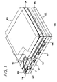
- the plane type display device 100 shown in Figure 1 is comprised of a body 102 of plane type white colour light emitting display device having a white colour light emitting fluorescent screen 101 and field emission type cathodes K arranged opposite thereto as well as a plane type colour shutter 103 arranged adjacent or opposite to the front face of the screen 101 on its arranged side.
- the display device body 102 is constructed in such a manner that a transparent front panel 104 and a rear panel 105 oppose to each other through a spacer (not shown ) holding a predetermined space between both panels 104 and 105 and the peripheries thereof are sealed airtightly by the glass frit, etc. to form a flat space between the panels 104 and 105.
- the white colour light emitting screen 101 which is made by applying previously a white colour light emitting fluorescencer entirely, and its surface is coated with a metal-backed layer 106 of aluminum film, etc. as in the ordinary cathode ray tube.
- cathode electrodes 107 which, for example, extend vertically in the shape of belts.
- cathode electrodes 107 are covered with an insulation layer 108, on which gate electrodes 109 that extend, for example, in the horizontal direction nearly perpendicular to the extension direction of cathode electrodes 107 are arranged in parallel.
- each electrode 107 and each gate electrode 109 are bored openings 110, in which conical field emission type cathodes K are formed on the cathodes 107, respectively.
- This field emission type cathode K is made of such materials that electron emission occurs due to the tunnel effect by impressing the electric field, e.g. on the level of 10 6 to 10 7 [ v/cm] on molybdenum, tungsten, chromium and so on.
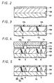
- cathode structure including the field emission type cathode K and the gate electrode, etc. forming the prior art plane type display device will be described together with an example of its manufacturing process in reference to manufacturing process diagrams of Figure 2 to Figure 5.
- the cathode electrodes 107 are formed on the inner surface of the rear panel 105 along one direction, e.g. the vertical scanning direction.
- cathode electrodes 107 are formed into a predetermined pattern, e.g. by evaporating or sputtering a metal layer of chromium, etc. entirely and then etching it selectively by photolithography.
- this patterned cathode electrodes 107 are coated entirely with the insulation layer 108 by sputtering, etc. and further on this layer a metal layer 111 becoming finally the gate electrodes 109 is formed, e.g. by evaporating or sputtering the metals of high melting point such as molybdenum. tungsten, etc.
- a resist pattern by the photoresist, etc. is formed and using this as a mask the anisotropic etching, e.g. RIE ( reactive ion-beam etching ) is carried out on the metal layer 111 to form into the predetermined pattern, namely, to form the beltlike gate electrode 109 extending in the horizontal direction perpendicular to the extension of the cathode electrode 107 shown in Figure 1.
- RIE reactive ion-beam etching
- these small holes 111h for example, a chemical etching which exhibits no etching property to the gate electrode 109, i.e. the metal layer 111 but exhibits the isotropic etching property to the insulation layer 108 is carried out to form cavities 112 having an opening width greater than that of the small holes 111h with a depth over a whole thickness of the insulation layer 108.
- the gate electrode 109 is covered with a metal layer 113 made of, e.g. alminium, nickel, etc. by an oblique evaporation.
- This oblique evaporation is carried out while the rear panel 105 is rotated in its plane to form round holes 114 having a conical inner circumference around the small holes 111h.
- the evaporation of metal layer 113 is carried out at such a selected angle that the inside of cavities 112 may not be coated through the small holes 111h.
- a field emission type cathode material namely, a metal having a high melting point and a low work function such as tungsten, molybdenum, etc. is adhered through the round holes 114 on the cathode electrode 107 inside the cavities 112 at right angles to this cathode electrode surface by evaporation, sputtering and so on.
- a field emission type cathode material namely, a metal having a high melting point and a low work function such as tungsten, molybdenum, etc.
- the cathodes K are surrounded by the insulation layer 108 and therefore insulated electrically from the cathode electrode 107.
- the gate electrodes 109 In opposition to each cathode K are arranged the gate electrodes 109 through which the aforesaid small holes 111h are bored as an electron passing holes. In this way, the cathode structure is constructed.
- the cathode structure in which the field emission type cathode K is thus formed on the cathode electrode 107 and the gate electrode 109 is further formed above and across the cathode K is arranged in opposition to the white colour screen 101.
- the fluorescent screen 101 i.e. the metal-backed layer 106 is given a high anode voltage being positive to the cathode and also, for example, between the cathode electrode 107 and the gate electrode 109 is impressed a voltage which enables electrons to be emitted sequentially from the field emission type cathode at their intersection.
- a voltage of 100 v relative to the cathode electrode 107 impressed on the gate electrode 109 is modulated in sequence according to display contents in order to direct the resulting electron beam from the tip of cathode K towards the white colour fluorescent screen 101.
- a white colour image of light emitting pattern corresponding to each colour can be obtained in the time division manner by the display device body 102, and at the same time the colour shutter 103 is switched in synchronism with that time division display to derive a light corresponding to each colour.
- optical images of red, green and blue are derived in sequence to display a colour picture as a whole.
- the field emission type cathode K opposing to the fluorescent screen is formed into a cone whose section is a triangular form due to the manufacturing process described referring to Figure 2 to Figure 5, thus causing the electric field to concentrate on the tip of the cone for raising the electron emission.
- the cathode K when the cathode K is formed as described referring to Figures 2 to 5, its tip will have a shape whose radius of curvature is relatively gradual to the extent that the radius of curvature at the tip is dozens of n m, e.g. about sixty n m. In order to aim at the latest high resolution, it is needed to form this further finely for efficient electric field concentration and electron emission.
- the present inventors et al have repeated studying devotedly and, as a result, come to provide a field emission type cathode, an electron emitting apparatus and a process for manufacturing the electron emitting apparatus in which the field emission type cathode K forming the plane type display device is made finer and sharper to enable further efficient concentration of electric field.
- the field emission type cathode according to the present invention has a multilayered structure in which conductive platelike corpuscles are piled.
- the electron emitting apparatus is such that the field emission type cathodes are arranged in opposition to the fluorescent screen and each of the cathodes has a multilayered structure in which the conductive platelike corpuscles are piled. By applying a predetermined electric field to the cathode, electrons will be emitted from its end surface.
- the process for manufacturing the electron emitting apparatus has steps of forming a pile of layers of conductive platelike corpuscles made into the multilayered structure by piling the conductive platelike corpuscles on the field emission type cathode forming surface constituting the electron emitting apparatus, and forming an edge portion for concentrating the electric field on the end surface of layered pile of platelike corpuscles by pattern-etching the layered pile of platelike corpuscles
- the field emission type cathode K is made up of the layered pile of platelike corpuscles, the electron emitting portion of the cathode K is made finer and sharper, thereby causing the efficient concentration of electric field and enhancing the efficiency of electron emission.
- the field emission type cathode according to the present invention is formed into the multilayered structure in which the conductive platelike corpuscles are piled.
- the electron emitting apparatus is such that the field emission type cathodes are arranged in opposition to the fluorescent screen and each of them has the multilayered structure in which the conductive platelike corpuscles are piled. It is arranged in such a manner that a predetermined electric field is applied to the cathode, thereby causing electrons to be emitted from its end surface.
- the plane type display device 20 shown in Figure 6 is comprised of a plane type light emitting display body 2 having a light emitting fluorescent screen 1 and field emission type cathodes K arranged opposite thereto, and a plane type colour shutter 3 arranged adjacent or opposite to the front face of the fluorescent screen I on its arranged side.
- the display device body 2 is constructed in the same way as described with Figure 1 so that as shown in Figure 6 a transparent front panel 4 and a rear panel 5 oppose to each other through a spacer (not shown ) holding a predetermined space between both panels 4 and 5, and the periphery thereof is sealed airtightly by the glass frit, etc. to form a flat space between the panels 4 and 5.
- the light emitting fluorescent screen 1 which is made by applying beforehand a light emitting fluorescencer entirely, and its surface is coated with an anode metal layer 60 and a metal-backed layer 6 made of alminium film, etc. as in the ordinary cathode ray tube.
- cathode electrodes 7 which, for example, extend vertically in the shape of belts.
- Gate electrodes 9 are arranged and mounted in parallel through an insulation layer 8, for example, in the horizontal direction nearly perpendicular to the extension direction of these cathode electrodes 7.
- the field emission type cathode K is formed on each cathode electrode 7 and midway between the plural gate plural electrodes 9, respectively.
- Figure 7 is a schematic diagram showing the relative positional relationship among the cathode electrode 7, the gate electrode 9 and the field emission type cathode K. Additionally, in Figure 7, although an example in which two field emission type cathodes K are formed on the cathode electrode 7 between the gate electrodes 9 is shown, the present invention is not limited to this example.
- Figure 8 is a schematic sectional diagram showing the relative positional relationship among the cathode electrode 7, the gate electrode 9 and the field emission type cathode K.
- the gate electrode 9 can also be formed through a dielectric layer 19.
- This field emission type cathode K is composed of a pile of layers of platelike corpuscles 30 each made of combined carbon, e.g. graphite, amorphous carbon, diamond-shape like carbon, etc. which has a shape as shown in Figure 9.
- the corpuscle 30 e.g. those having a diameter of 500 nm and a thickness of 20 nm or so may be employed.
- This platelike corpuscle forming the field emission type cathode K has, for example, a shape of almost circular plate, an average particle diameter of five ⁇ m or less, and an average aspect ratio ( a value of the square root of an area of a platelike corpuscle divided by its thickness ) of five or more.
- the particle diameter is three ⁇ m or less, the corpuscles whose diameter is 0.1 ⁇ m or less occupying 40 to 95 weight percent of whole platelike corpuscles forming the cathode, the average particle diameter of platelike corpuscles forming the field emission type cathode K being between 0.05 ⁇ m and 0.08 ⁇ m and the average aspect ratio ( a value of the square root of an area of a platelike corpuscle divided by its thickness ) being ten or more.
- the particle diameter is stokes diameter and was measured, e.g. by a centrifugal sedimentation method light transmission type particle size distribution apparatus.
- the field emission type cathode K is composed of the pile of layers of platelike corpuscles as shown in Figure 9.
- a particle size of the corpuscle 30 if its average particle diameter is greater than five ⁇ m, then the edge portion of end surface of the layered pile will become so gradual that it will be difficult to make the efficient concentration of electric field and electron emission.
- most of the corpuscles preferably have the particle diameter of 0.1 ⁇ m or less. If an amount of the corpuscles whose particle diameter is 0.1 ⁇ m or less is smaller than 40 weight percent, it will then be difficult to form a uniform coating film so that a shape of the cathode K will become undesirably non-uniform. Therefore, it is preferable that the average particle diameter is on the level of 0.05 to 0.08 ⁇ m. Additionally, the particle size distribution can be measured by the light transmission type particle size distribution measuring apparatus.
- V at the tip of cathode K is equal to a threshold voltage Vt of electron emission of the field emission type cathode K.
- a voltage of a cathode driving circuit is desirably between dozens of volts and one hundred volts from the viewpoint of performance and price of transistor.
- a threshold electric field Et corresponding to V t depends on the homogeneity. For metal materials it is 10 7 [V /cm] or less. For carbonic system materials it is 10 6 [ V/cm] or less.
- dimensions of the corpuscle in its plate surface direction depend on the size of emitter.
- the size of emitter depends in turn on dimensions of a displayed pixel of the display device.
- the dimensions of the displayed pixel depend on display dimensions and the density of pixel ( resolution ).
- resolution the number of pixels is 1024 x 768 and the size of one subpixel is approximately 60[ ⁇ m] x 100 [ ⁇ m].
- the size of one emitter becomes about a dozen [ ⁇ m] to several [ ⁇ m]. It is necessary for the size of corpuscle to be submicron, i.e. 0.1 to 0.5 [ ⁇ m] or so, in order to pattern precisely emitters of the size on this level.
- the average aspect ratio is five or more, desirably ten or more.
- the scalelike corpuscles shown in Figure 9, namely, the platelike corpuscles 30 are, for example, dispersed in a solvent 31 such as water, organic solvent and the like.
- the resulting substance is applied to a cathode forming surface 32, for example, by means of a spinner, a coater, etc. as shown in Figure 5.
- thermosetting resin etc. may be mixed into the solvent 31.
- the scalelike corpuscles sink naturally and as is shown in Figure 11, the scalelike corpuscles, i.e. platelike corpuscles 30 settle on the cathode forming surface 32 and pile in layers which lie nearly along the forming surface. Subsequently, it is prebaked to form a pile of layers 33 of platelike corpuscles.
- a photoresist 34 is applied onto the layered pile 33 of platelike corpuscles. This is dried and then pattern-exposed, e.g. by a high voltage mercury lamp to form into a predetermined pattern by developing it, e.g. using alkali developing solution.
- any one of the negative photoresist and the positive photoresist can be employed as this photoresist.
- a novolac type of positive photoresist PMER 6020 EK made by Tokyo Ohka Kogyo ), etc. can be employed.
- the pattern-etching is carried out on the pile of layers 33 using the photoresist as an etching mask to form a layered pile pattern 33a.
- any one of acid and alkali can be employed.
- the patter-etching can also be performed by blowing pure water with high pressure by a spray.
- the photoresist 34 is removed and then the post-baking is carried out to stabilize the layered pile pattern 33a of platelike corpuscle.
- Figure 15 is an enlarged schematic diagram of the layered pile pattern 33a of platelike corpuscle.
- the layered pile pattern 33a is such that the platelike corpuscles are piled in layers, on its end surface appears an edge portion 30a, e.g. about 20 nm thick, of the platelike corpuscle.
- this edge portion 30a it is possible to form the field emission type cathode K having the edge portion whose curvature radius is 20 [ nm ] or less, for example, in case of the corpuscle of 20 [ nm ] in thickness, which curvature radius is equal to or far smaller than that of the tip of the prior art field emission type cathode K, i.e. the conical cathode K which was shown in Figure 1 and whose manufacturing method was described with Figure 2 to Figure 5.
- the field emission type cathodes K are formed on the cathode electrodes 7, above and across which the gate electrodes 9 are further formed to make the cathode structure, which is arranged in opposition to the fluorescent screen 1.
- a positive high anode voltage against the cathode is given to the fluorescent screen 1, i.e. the anode metal layer 60 and also between the cathode electrode 7 and the gate electrode 9, for example, a voltage which enables electrons to be emitted in sequence from the field emission type cathodes K at their intersections is impressed.
- a voltage of 100 V relative to the cathode electrode 7 impressed to the gate electrode 9 is modulated in sequence according to the display contents, thus causing the resulting beam of electron e- from the edge portion 30a of the cathode K to be directed towards the fluorescent screen 1.
- the white colour image of light emission pattern corresponding to each colour can be obtained in the time division style by the display device body 2, and at the same time the colour shutter 3 is switched in synchronism with that time division display to derive a light corresponding to each colour.
- optical images of red, green and blue are derived sequentially to display a colour picture as a whole.
- the electron emitting apparatus 40 of the present invention by making the field emission type cathode K formed on the cathode electrode 7 into the multilayered structure in which the conductive platelike corpuscles 30 are piled as shown in Figure 15, it is possible to create the edge portion 30a of the end surface of field emission type cathode K concentrating the electric field so as to have the sharpness which is equal to or more than that of the tip of conventional conical field emission type cathode K by the easy manufacturing process, thereby allowing electron to be emitted efficiently and thus allowing an electron emitting apparatus with high accuracy to be provided.
- the display device can be constructed in such a manner that, in addition to the example having the white colour light emission fluorescent screen, the fluorescent screen of red, green and blue are each separated.
- the structure of display device can appropriately be altered.
- the present invention is not limited to this example. As is shown in Figure 18, it is also applicable as well to a case where an insulation layer 18 is entirely formed on the cathode electrode 7 and then a predetermined part of this insulation layer is bored, the field emission type cathode K being made conductive with the cathode electrode 7 lying under the bored part by connecting both of them to each other through the bore with a conductive layer 17 made of tungsten or the like.
- the present invention is not restricted to this example and is also applicable to a case as well where it is formed on a plane having a predetermined unevenness.
- the field emission type cathode and the electron emitting apparatus of the present invention by making the field emission type cathode K formed on the cathode electrode 7 as the pile of layers 33 in which the conductive platelike corpuscles 30 are piled in the multilayered structure, it will be possible to create the edge portion 30a of end surface of the field emission type cathode K for concentrating the electric field with its sharpness which is equal to or more than that of the tip of the prior art conical field emission type cathode K in order to enable an efficient electron emission, thus allowing an electron emitting apparatus with high accuracy to be provided.
- the process for manufacturing the electron emitting apparatus of the present invention by making the field emission type cathode K formed on the cathode electrode 7 as the pile of layers 33 in which the conductive platelike corpuscles 30 are piled in the multilayered structure, it will be possible to form the edge portion 30a of end surface of the field emission type cathode K for concentrating the electric field with its sharpness which is equal to or more than that of the tip of the prior art conical field emission type cathode K by easy manufacturing processes, thereby enabling an efficient electron emission and an electron emitting apparatus with high accuracy to be provided.
Landscapes
- Engineering & Computer Science (AREA)
- Manufacturing & Machinery (AREA)
- Cold Cathode And The Manufacture (AREA)
- Cathode-Ray Tubes And Fluorescent Screens For Display (AREA)
- Electrodes For Cathode-Ray Tubes (AREA)
Applications Claiming Priority (2)
| Application Number | Priority Date | Filing Date | Title |
|---|---|---|---|
| JP35792898 | 1998-12-16 | ||
| JP35792898A JP2000182508A (ja) | 1998-12-16 | 1998-12-16 | 電界放出型カソード、電子放出装置、および電子放出装置の製造方法 |
Publications (2)
| Publication Number | Publication Date |
|---|---|
| EP1030338A2 true EP1030338A2 (de) | 2000-08-23 |
| EP1030338A3 EP1030338A3 (de) | 2002-06-12 |
Family
ID=18456661
Family Applications (1)
| Application Number | Title | Priority Date | Filing Date |
|---|---|---|---|
| EP99403176A Withdrawn EP1030338A3 (de) | 1998-12-16 | 1999-12-16 | Feldemissionskathode, Apparat mit einer solchen Kathode und Verfahren zur Herstellung des Apparats |
Country Status (3)
| Country | Link |
|---|---|
| US (2) | US6600262B1 (de) |
| EP (1) | EP1030338A3 (de) |
| JP (1) | JP2000182508A (de) |
Cited By (1)
| Publication number | Priority date | Publication date | Assignee | Title |
|---|---|---|---|---|
| US7569861B2 (en) | 2002-08-29 | 2009-08-04 | Seoul Semiconductor Co., Ltd. | Light emitting device having light emitting elements |
Families Citing this family (4)
| Publication number | Priority date | Publication date | Assignee | Title |
|---|---|---|---|---|
| JP2001185019A (ja) | 1999-12-27 | 2001-07-06 | Hitachi Powdered Metals Co Ltd | 電界放出型カソード、電子放出装置、及び電子放出装置の製造方法 |
| JP2003086079A (ja) * | 2001-09-13 | 2003-03-20 | Sony Corp | 電子放出装置及びその製造方法、冷陰極電界電子放出素子及びその製造方法、並びに、冷陰極電界電子放出表示装置及びその製造方法 |
| TWI309842B (en) * | 2006-06-19 | 2009-05-11 | Tatung Co | Electron emission source and field emission display device |
| TWI309843B (en) | 2006-06-19 | 2009-05-11 | Tatung Co | Electron emission source and field emission display device |
Family Cites Families (16)
| Publication number | Priority date | Publication date | Assignee | Title |
|---|---|---|---|---|
| US3936697A (en) * | 1974-04-25 | 1976-02-03 | Texas Instruments Incorporated | Charged particle beam scanning device |
| JPH03203776A (ja) | 1989-12-29 | 1991-09-05 | Sharp Corp | 強誘電性液晶パネルの表示制御装置 |
| KR940008180B1 (ko) | 1990-12-27 | 1994-09-07 | 가부시끼가이샤 한도다이 에네르기 겐꾸쇼 | 액정 전기 광학 장치 및 그 구동 방법 |
| US5675216A (en) * | 1992-03-16 | 1997-10-07 | Microelectronics And Computer Technololgy Corp. | Amorphic diamond film flat field emission cathode |
| EP0675519A1 (de) | 1994-03-30 | 1995-10-04 | AT&T Corp. | Vorrichtung mit Feldeffekt-Emittern |
| US5499062A (en) | 1994-06-23 | 1996-03-12 | Texas Instruments Incorporated | Multiplexed memory timing with block reset and secondary memory |
| EP0706196B1 (de) * | 1994-10-05 | 2000-03-01 | Matsushita Electric Industrial Co., Ltd. | Elektronenemissionskathode; eine Elektronenemissionsvorrichtung, eine flache Anzeigevorrichtung, eine damit versehene thermoelektrische Kühlvorrichtung, und ein Verfahren zur Herstellung dieser Elektronenemissionskathode |
| FR2726688B1 (fr) * | 1994-11-08 | 1996-12-06 | Commissariat Energie Atomique | Source d'electrons a effet de champ et procede de fabrication de cette source, application aux dispositifs de visualisation par cathodoluminescence |
| US5616368A (en) | 1995-01-31 | 1997-04-01 | Lucent Technologies Inc. | Field emission devices employing activated diamond particle emitters and methods for making same |
| US5709577A (en) | 1994-12-22 | 1998-01-20 | Lucent Technologies Inc. | Method of making field emission devices employing ultra-fine diamond particle emitters |
| US5959598A (en) | 1995-07-20 | 1999-09-28 | The Regents Of The University Of Colorado | Pixel buffer circuits for implementing improved methods of displaying grey-scale or color images |
| JP3421549B2 (ja) | 1996-09-18 | 2003-06-30 | 株式会社東芝 | 真空マイクロ装置 |
| US6356014B2 (en) * | 1997-03-27 | 2002-03-12 | Candescent Technologies Corporation | Electron emitters coated with carbon containing layer |
| WO1999066523A1 (en) * | 1998-06-18 | 1999-12-23 | Matsushita Electric Industrial Co., Ltd. | Electron emitting device, electron emitting source, image display, and method for producing them |
| JP2000268706A (ja) * | 1999-03-18 | 2000-09-29 | Matsushita Electric Ind Co Ltd | 電子放出素子及びそれを用いた画像描画装置 |
| JP2000306492A (ja) * | 1999-04-21 | 2000-11-02 | Hitachi Powdered Metals Co Ltd | 電界放出型カソード、電子放出装置、および電子放出装置の製造方法 |
-
1998
- 1998-12-16 JP JP35792898A patent/JP2000182508A/ja active Pending
-
1999
- 1999-12-13 US US09/458,830 patent/US6600262B1/en not_active Expired - Fee Related
- 1999-12-16 EP EP99403176A patent/EP1030338A3/de not_active Withdrawn
-
2003
- 2003-05-12 US US10/435,480 patent/US20030205959A1/en not_active Abandoned
Cited By (13)
| Publication number | Priority date | Publication date | Assignee | Title |
|---|---|---|---|---|
| US7569861B2 (en) | 2002-08-29 | 2009-08-04 | Seoul Semiconductor Co., Ltd. | Light emitting device having light emitting elements |
| US7615793B2 (en) | 2002-08-29 | 2009-11-10 | Seoul Semiconductor Co., Ltd. | AC driven light—emitting device |
| US7646031B2 (en) | 2002-08-29 | 2010-01-12 | Seoul Semiconductor Co., Ltd. | Light emitting device having light emitting elements |
| US7667237B2 (en) | 2002-08-29 | 2010-02-23 | Seoul Semiconductor Co., Ltd. | Light emitting device having light emitting elements |
| US7897982B2 (en) | 2002-08-29 | 2011-03-01 | Seoul Semiconductor Co., Ltd. | Light emitting device having common N-electrode |
| US7956367B2 (en) | 2002-08-29 | 2011-06-07 | Seoul Semiconductor Co., Ltd. | Light-emitting device having light-emitting elements connected in series |
| US8084774B2 (en) | 2002-08-29 | 2011-12-27 | Seoul Semiconductor Co., Ltd. | Light emitting device having light emitting elements |
| US8097889B2 (en) | 2002-08-29 | 2012-01-17 | Seoul Semiconductor Co., Ltd. | Light emitting device having light emitting elements with a shared electrode |
| US8129729B2 (en) | 2002-08-29 | 2012-03-06 | Seoul Semiconductor Co., Ltd. | Light emitting device having light emitting elements and an air bridge line |
| US8680533B2 (en) | 2002-08-29 | 2014-03-25 | Seoul Semiconductor Co., Ltd. | Light-emitting device having light-emitting elements with a shared electrode |
| US8735911B2 (en) | 2002-08-29 | 2014-05-27 | Seoul Semiconductor Co., Ltd. | Light emitting device having shared electrodes |
| US8735918B2 (en) | 2002-08-29 | 2014-05-27 | Seoul Semiconductor Co., Ltd. | Light-emitting device having light-emitting elements with polygonal shape |
| US9947717B2 (en) | 2002-08-29 | 2018-04-17 | Seoul Semiconductor Co., Ltd. | Light-emitting device having light-emitting elements and electrode spaced apart from the light emitting element |
Also Published As
| Publication number | Publication date |
|---|---|
| US6600262B1 (en) | 2003-07-29 |
| EP1030338A3 (de) | 2002-06-12 |
| JP2000182508A (ja) | 2000-06-30 |
| US20030205959A1 (en) | 2003-11-06 |
Similar Documents
| Publication | Publication Date | Title |
|---|---|---|
| KR100286828B1 (ko) | 플랫패널표시장치 | |
| EP1047096B1 (de) | Feldemissionskathode, Elektronenemissionsvorrichtung und Verfahren zur Herstellung | |
| US5509839A (en) | Soft luminescence of field emission display | |
| US6028391A (en) | Field emission device having spherically curved electron emission layer and spherically recessed substrate | |
| JPH11232997A (ja) | 電子放出装置及びその製造方法 | |
| KR100343222B1 (ko) | 전계방출표시소자의제조방법 | |
| US5880554A (en) | Soft luminescence of field emission display | |
| US5595519A (en) | Perforated screen for brightness enhancement | |
| US7473154B2 (en) | Method for manufacturing carbon nanotube field emission display | |
| JP3253683B2 (ja) | 電界放出型冷陰極板の製造方法 | |
| US6737792B2 (en) | Field emission cathode, electron emission device and electron emission device manufacturing method | |
| US6600262B1 (en) | Field emission type cathode and electron emitting apparatus using piled platelike particles | |
| JP4206858B2 (ja) | 電界電子放出素子 | |
| US5463273A (en) | Dimpled image display faceplate for receiving multiple discrete phosphor droplets and having conformal metallization disposed thereon | |
| US5785873A (en) | Low cost field emission based print head and method of making | |
| KR100565200B1 (ko) | 탄소 나노튜브 전계방출소자 및 제조방법 | |
| KR100464306B1 (ko) | 전계방출표시소자및그스페이서제조방법 | |
| JP3082290B2 (ja) | 平面型表示装置 | |
| KR100343212B1 (ko) | 수평전계효과전자방출소자및그제조방법 | |
| KR970010990B1 (ko) | 전계전자방출소자 및 그의 제조방법 | |
| KR100627255B1 (ko) | 전계방출구조 및 그 제조방법_ | |
| KR20070056614A (ko) | 전자 방출 디바이스의 제조 방법 | |
| JPH0757667A (ja) | 電界放出型ディスプレイ装置 | |
| KR20050077960A (ko) | 전계 방출 표시장치 | |
| KR20030061173A (ko) | 전계 방출 디바이스를 이용한 프로젝션 장치 |
Legal Events
| Date | Code | Title | Description |
|---|---|---|---|
| PUAI | Public reference made under article 153(3) epc to a published international application that has entered the european phase |
Free format text: ORIGINAL CODE: 0009012 |
|
| AK | Designated contracting states |
Kind code of ref document: A2 Designated state(s): AT BE CH CY DE DK ES FI FR GB GR IE IT LI LU MC NL PT SE |
|
| AX | Request for extension of the european patent |
Free format text: AL;LT;LV;MK;RO;SI |
|
| PUAL | Search report despatched |
Free format text: ORIGINAL CODE: 0009013 |
|
| AK | Designated contracting states |
Kind code of ref document: A3 Designated state(s): AT BE CH CY DE DK ES FI FR GB GR IE IT LI LU MC NL PT SE |
|
| AX | Request for extension of the european patent |
Free format text: AL;LT;LV;MK;RO;SI |
|
| RIC1 | Information provided on ipc code assigned before grant |
Free format text: 7H 01J 1/30 A, 7H 01J 3/02 B, 7H 01J 1/304 B, 7H 01J 9/02 B |
|
| 17P | Request for examination filed |
Effective date: 20021127 |
|
| AKX | Designation fees paid |
Designated state(s): FR GB |
|
| REG | Reference to a national code |
Ref country code: DE Ref legal event code: 8566 |
|
| 17Q | First examination report despatched |
Effective date: 20050304 |
|
| STAA | Information on the status of an ep patent application or granted ep patent |
Free format text: STATUS: THE APPLICATION IS DEEMED TO BE WITHDRAWN |
|
| 18D | Application deemed to be withdrawn |
Effective date: 20050701 |